
DREAM IDEA PLAN IMPLEMENTATION Present to Amirkabir University

DREAM IDEA PLAN IMPLEMENTATION
Present to: Amirkabir University of Technology (Tehran Polytechnic) & Semnan University Dr. Kourosh Kiani 2 Email: kkiani 2004@yahoo. com Email: Kourosh. kiani@aut. ac. ir Web: aut. ac. com
i(t) R 2 a + _ R 1 c d b R 3 R 4 v(t) + + _
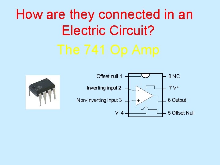
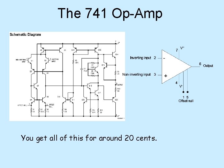
Operational Amplifier • Operational amplifier is an amplifier whose output voltage is proportional to the negative of its input voltage and that boosts the amplitude of an input signal, many times, i. e. , has a very high gain. High-gain amplifiers. • They were developed to be used in synthesizing mathematical operations in early analog computers, hence their name. • Typified by the series 741 (The integrated circuit contains 8 -pin mini-DIP, 20 transistors and 11 resistors). • Used for amplifications, as switches, as filters, as rectifiers, and in digital circuits. • Take advantage of large open-loop gain. • It is usually connected so that part of the output is fed back to the input. • Can be used with positive feedback to produce oscillation.
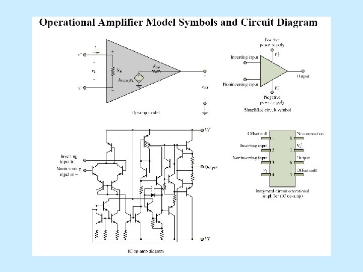
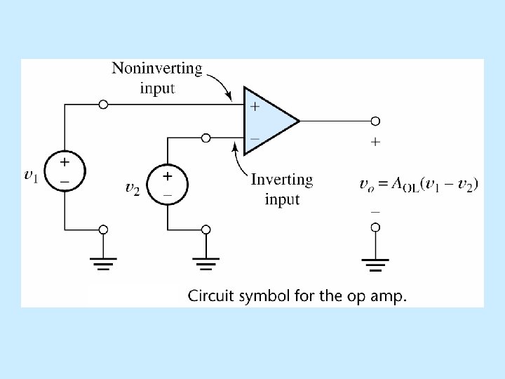
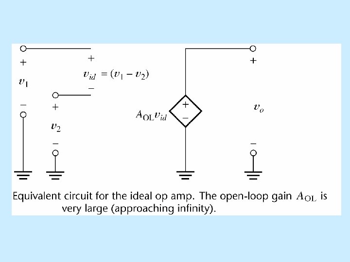
The Operational Amplifier • The integrated circuit operational amplifier evolved soon after development of the first bipolar integrated circuit. • The μA-709 was introduced by Fairchild Semiconductor in 1965. • Since then, a vast array of op-amps with improved characteristics, using both bipolar and MOS technologies, have been designed. • Most op amps are inexpensive (less than a dollar) and available from a wide range of suppliers. • There are usually 20 to 30 transistors that make up an op-amp circuit. • From a signal point of view, the op-amp has two input terminals and one output terminal as shown in the following figures. • The ideal op-amp senses the difference between two input signals and amplifies the difference to produce an output signal. • Ideally, the input impedance is infinite, which means that the input current is zero. The output impedance is zero.
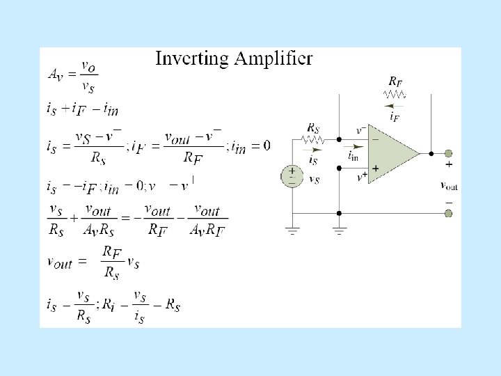
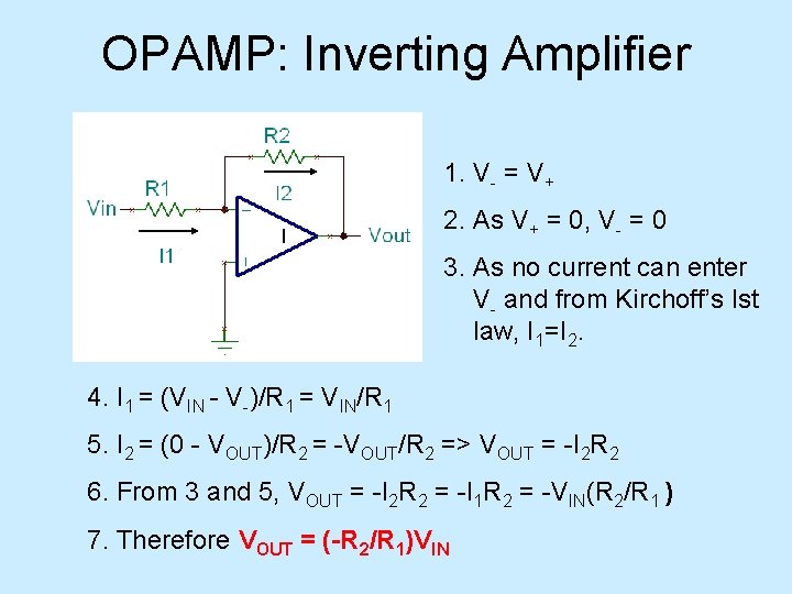
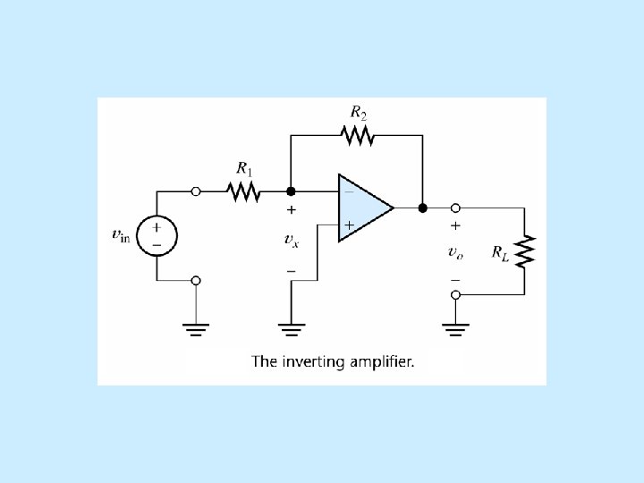
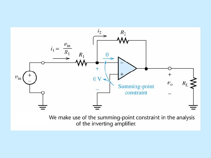
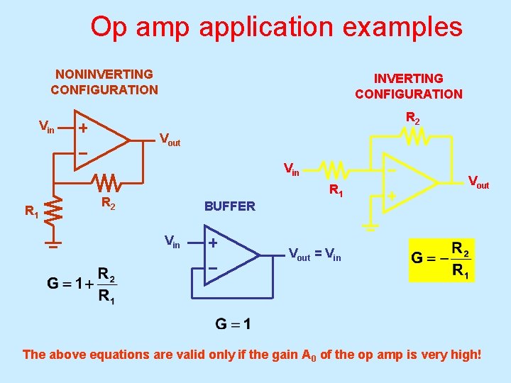
OPAMP: Inverting Amplifier 1. V- = V+ 2. As V+ = 0, V- = 0 3. As no current can enter V- and from Kirchoff’s Ist law, I 1=I 2. 4. I 1 = (VIN - V-)/R 1 = VIN/R 1 5. I 2 = (0 - VOUT)/R 2 = -VOUT/R 2 => VOUT = -I 2 R 2 6. From 3 and 5, VOUT = -I 2 R 2 = -I 1 R 2 = -VIN(R 2/R 1 ) 7. Therefore VOUT = (-R 2/R 1)VIN
Non-Ideal Characteristics • Offset – DC input is zero but output is not zero – Adjust using pins 1 and 5
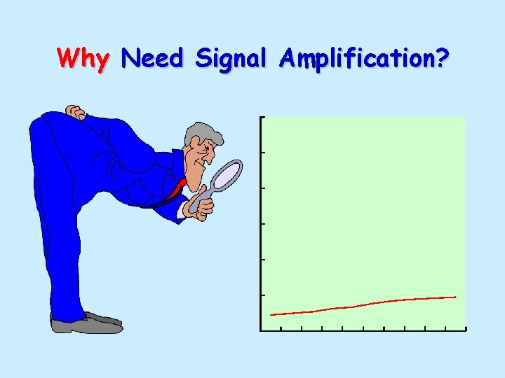
Why Need Signal Amplification?
Outlines of Signal Amplifiers l Designed to amplify input signals to a right level to be noticeable for further uses. l Typical input signals are: thermocouple, RTD, pressure, strain, flow, p. H, etc. l Typical outputs include: high level dc voltages (0 to 5 or 0 to 10 volts), process current (0 to 20 m. A or 4 to 20 m. A)
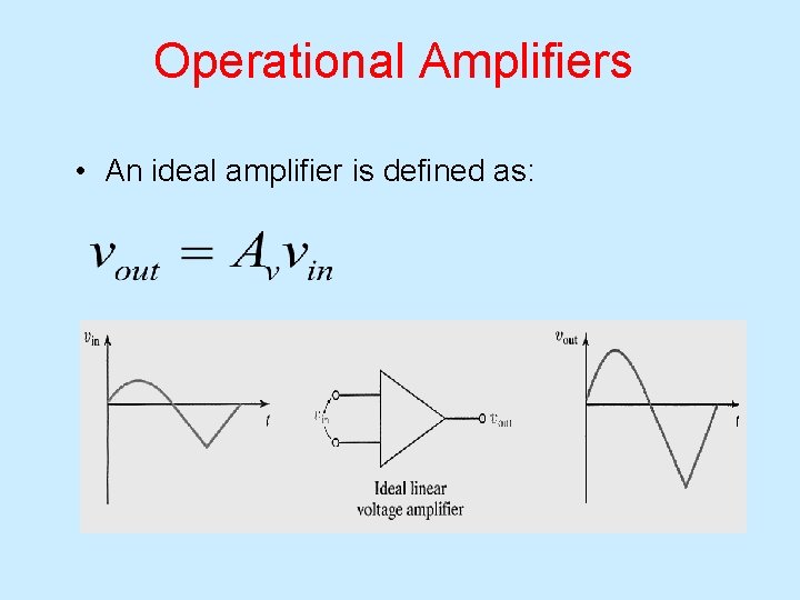
Operational Amplifiers • An ideal amplifier is defined as:
Operational Amplifier (“op-amp”) • Interconnection of transistors and resistors that vastly expands our capabilities in circuit design. • Used in a wide range of electronic circuits from engine control systems to cellular phones. • Designed to perform mathematical functions such as addition, subtraction, differentiation, integration, voltage scaling, current-to -voltage conversion, and a myriad of more complex applications.
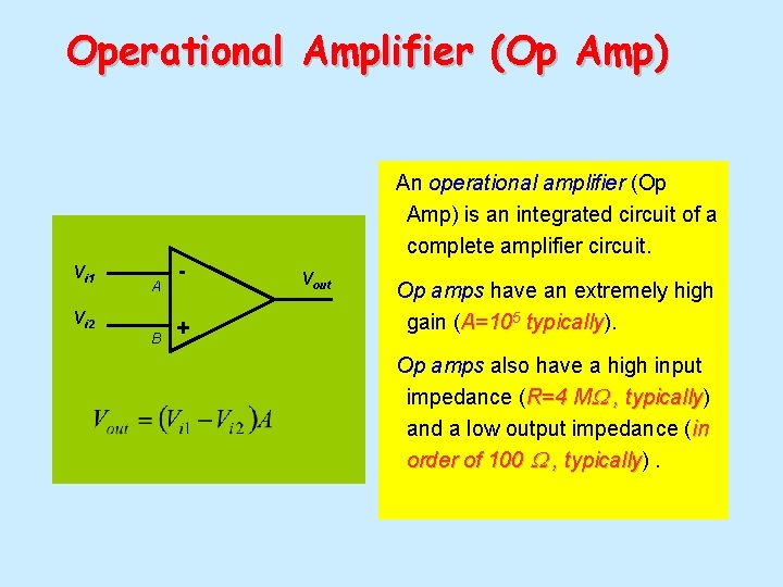
Operational Amplifier (Op Amp) An operational amplifier (Op Amp) is an integrated circuit of a complete amplifier circuit. Vi 1 Vi 2 A B + Vout Op amps have an extremely high gain (A=105 typically). typically Op amps also have a high input impedance (R=4 MW , typically) typically and a low output impedance (in order of 100 W , typically) typically.
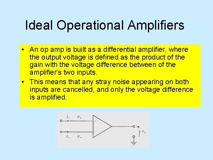
Ideal Operational Amplifiers • An op amp is built as a differential amplifier, where the output voltage is defined as the product of the gain with the voltage difference between of the amplifier’s two inputs. • This means that any stray noise appearing on both inputs are cancelled, and only the voltage difference is amplified.
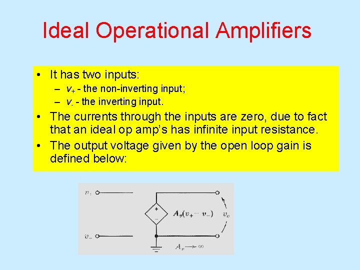
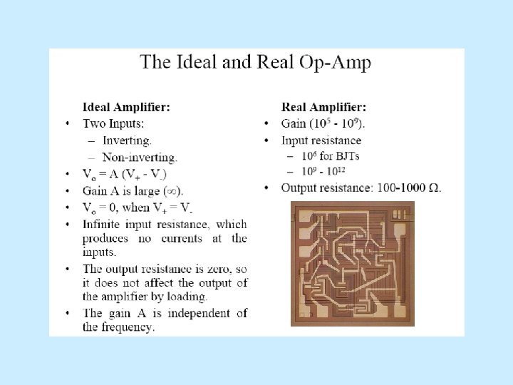
Ideal Operational Amplifiers • It has two inputs: – v+ - the non-inverting input; – v- - the inverting input. • The currents through the inputs are zero, due to fact that an ideal op amp’s has infinite input resistance. • The output voltage given by the open loop gain is defined below:
Negative Feedback • Negative feedback is required to make a large class of useful circuits with op amps. It is achieved when the output voltage, vo , is connected through a network to the inverting input of the op amp.
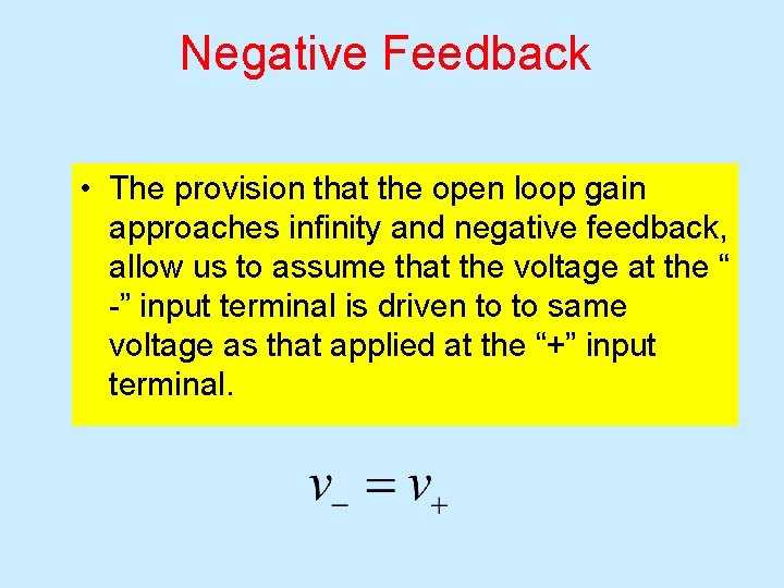
Negative Feedback • The provision that the open loop gain approaches infinity and negative feedback, allow us to assume that the voltage at the “ -” input terminal is driven to to same voltage as that applied at the “+” input terminal.
Closed Loop Gain • The negative feedback connection closes the loop, which allows us to compute the closed-loop gain, AF , for circuits containing such feedback loops.
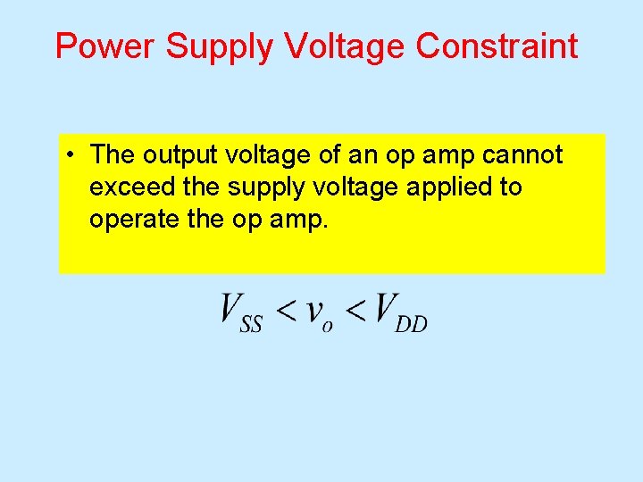
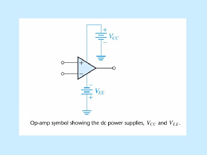
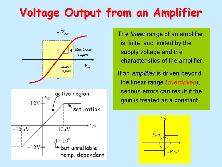
Power Supply Voltage Constraint • The output voltage of an op amp cannot exceed the supply voltage applied to operate the op amp.
Summary • An ideal op amp with feedback, assumes: – i+ = i- = 0 – v- = v+ – Vo is bounded by the power supply voltage.
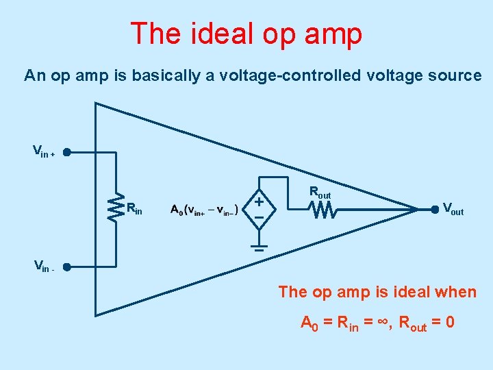
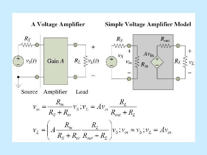
The ideal op amp An op amp is basically a voltage-controlled voltage source Vin + Rout Rin Vout Vin - The op amp is ideal when A 0 = Rin = ∞, Rout = 0
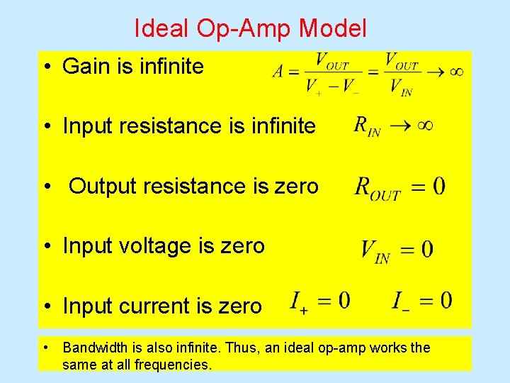
Ideal Op-Amp Model • Gain is infinite • Input resistance is infinite • Output resistance is zero • Input voltage is zero • Input current is zero • Bandwidth is also infinite. Thus, an ideal op-amp works the same at all frequencies.
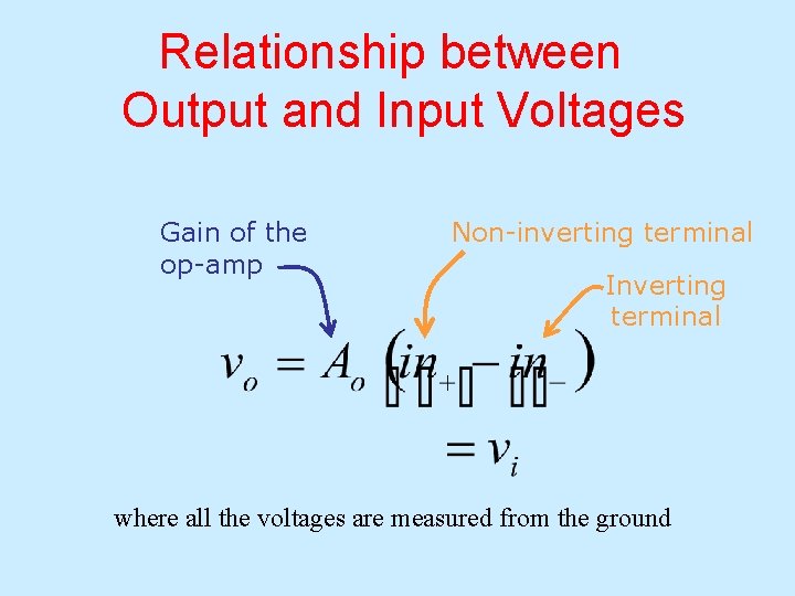
Relationship between Output and Input Voltages Gain of the op-amp Non-inverting terminal Inverting terminal where all the voltages are measured from the ground
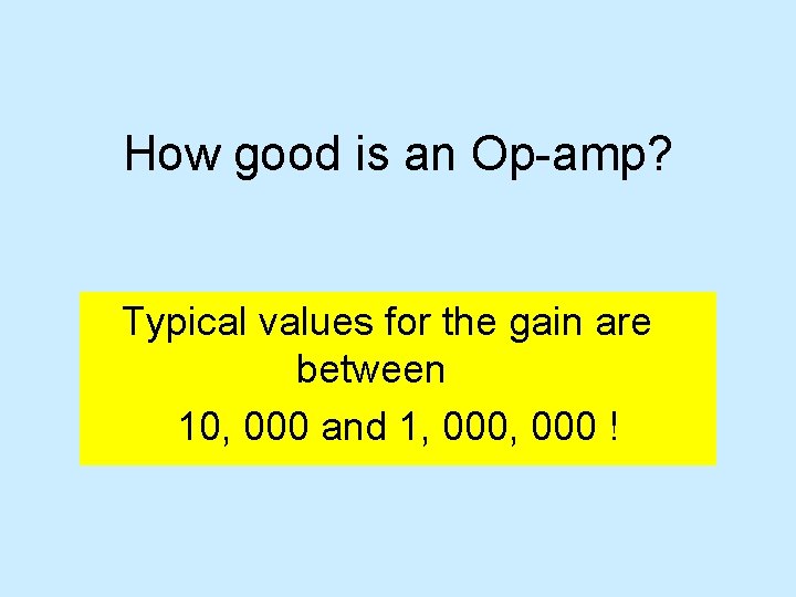
How good is an Op-amp? Typical values for the gain are between 10, 000 and 1, 000 !
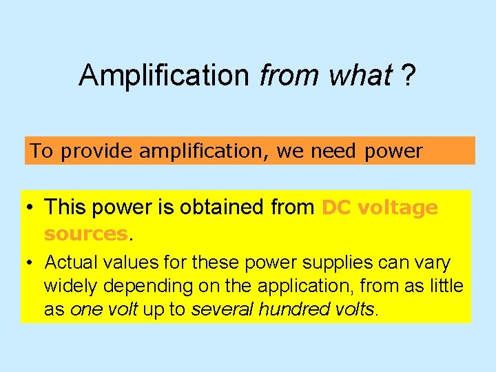
Amplification from what ? To provide amplification, we need power • This power is obtained from DC voltage sources. • Actual values for these power supplies can vary widely depending on the application, from as little as one volt up to several hundred volts.
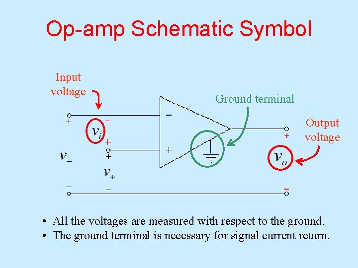
Op-amp Schematic Symbol Input voltage Ground terminal Output voltage • All the voltages are measured with respect to the ground. • The ground terminal is necessary for signal current return.
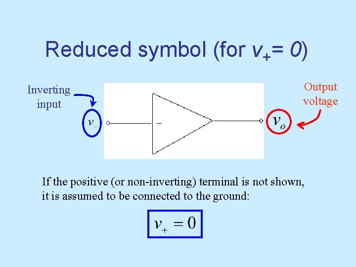
Reduced symbol (for v+= 0) Inverting input Output voltage If the positive (or non-inverting) terminal is not shown, it is assumed to be connected to the ground:
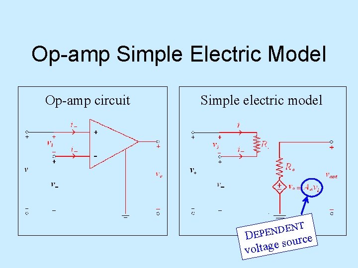
Op-amp Simple Electric Model Op-amp circuit Simple electric model NT E D N E D EP vo e c r u o s ltage
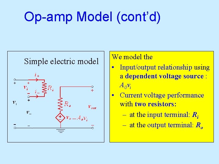
Op-amp Model (cont’d) Simple electric model We model the • Input/output relationship using a dependent voltage source : A 0 vi • Current voltage performance with two resistors: – at the input terminal: Ri – at the output terminal: Ro
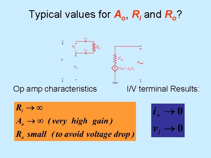
Typical values for Ao, Ri and Ro? Op amp characteristics I/V terminal Results:
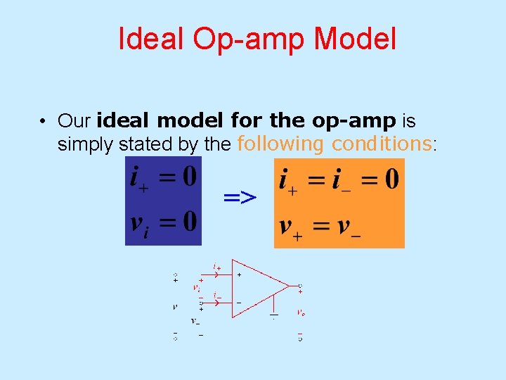
Ideal Op-amp Model • Our ideal model for the op-amp is simply stated by the following conditions: =>
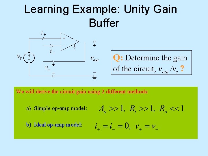
Learning Example: Unity Gain Buffer Q: Determine the gain of the circuit, vout /vs ? We will derive the circuit gain using 2 different methods: a) Simple op-amp model: b) Ideal op-amp model:
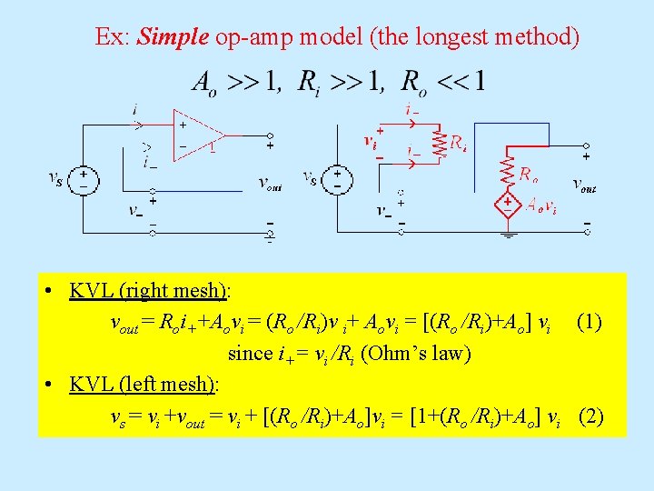
Ex: Simple op-amp model (the longest method) • KVL (right mesh): vout = Roi++Aovi = (Ro /Ri)v i+ Aovi = [(Ro /Ri)+Ao] vi (1) since i+= vi /Ri (Ohm’s law) • KVL (left mesh): vs = vi +vout = vi + [(Ro /Ri)+Ao]vi = [1+(Ro /Ri)+Ao] vi (2)
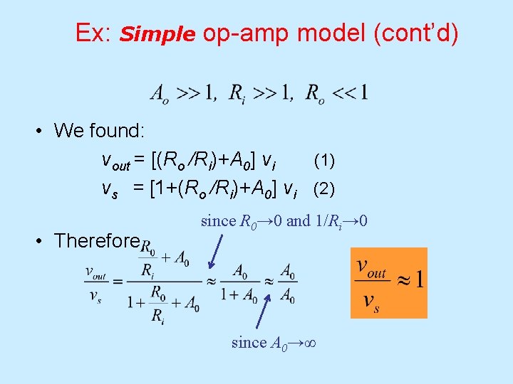
Ex: Simple op-amp model (cont’d) • We found: vout = [(Ro /Ri)+A 0] vi (1) vs = [1+(Ro /Ri)+A 0] vi (2) • Therefore, since R 0→ 0 and 1/Ri→ 0 => since A 0→∞
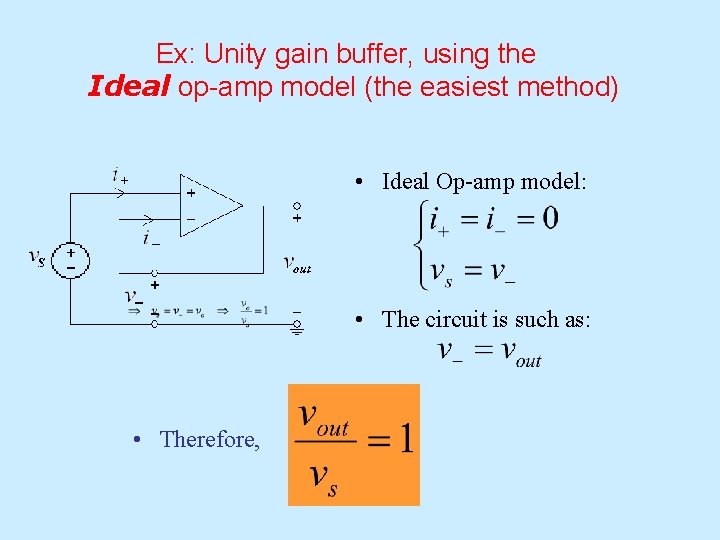
Ex: Unity gain buffer, using the Ideal op-amp model (the easiest method) • Ideal Op-amp model: • The circuit is such as: • Therefore,
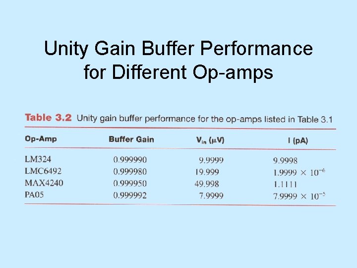
Unity Gain Buffer Performance for Different Op-amps
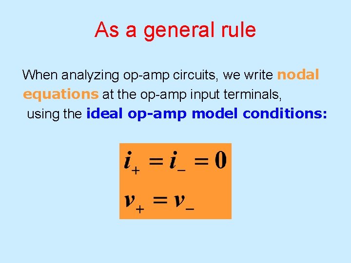
As a general rule When analyzing op-amp circuits, we write nodal equations at the op-amp input terminals, using the ideal op-amp model conditions:

Recall Unity Gain Buffer Example If vs = vout Ø Why not just connect vs to vout via two parallel connection wires ? Ø Why do we need to place an op-amp between them ?
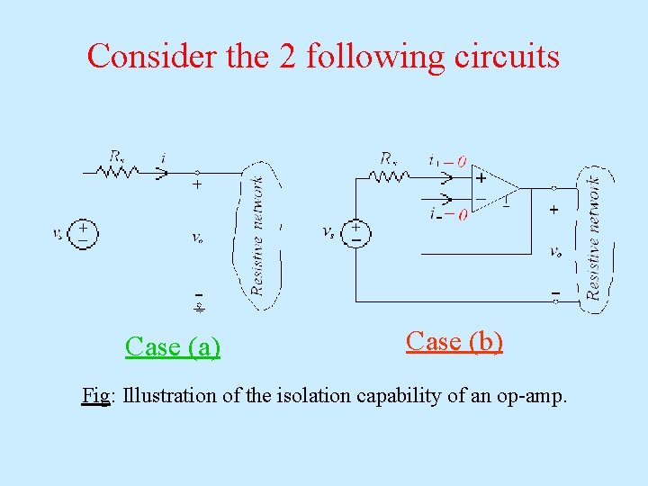
Consider the 2 following circuits Case (a) Case (b) Fig: Illustration of the isolation capability of an op-amp.
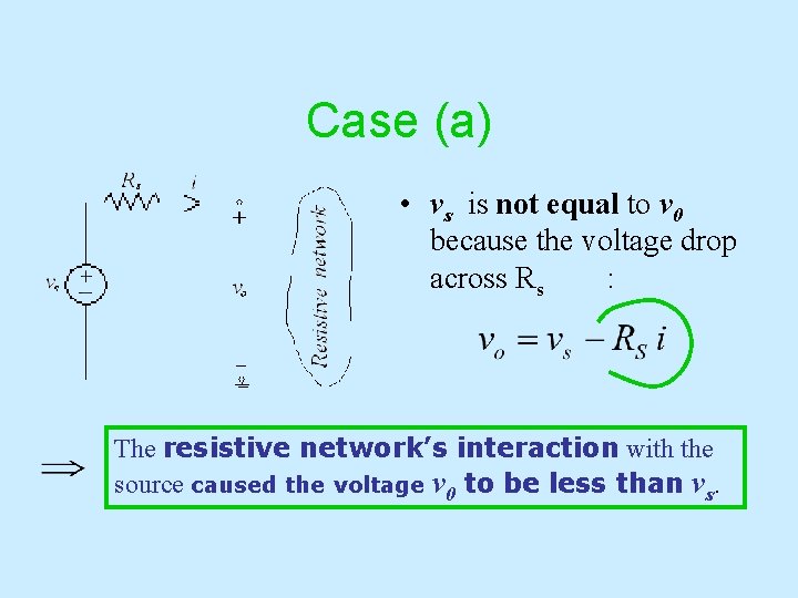
Case (a) • vs is not equal to v 0 because the voltage drop across Rs : The resistive network’s interaction with the source caused the voltage v 0 to be less than vs.
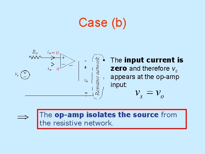
Case (b) • The input current is zero and therefore vs appears at the op-amp input: The op-amp isolates the source from the resistive network.
Note • In case (a), the energy supplied to the resistive network must come from the source. whereas • In case (b), it comes from the power that supplies the amplifier, and a little or no energy is drawn from vs.
R Op-Amp Circuit Applications • A number of R Op-amp circuits are designed to perform mathematical functions. • Classical R-Op-amp circuits: – Inverting amplifier – Differentiator amplifier – Summing amplifier – Precision differential voltage-gain device
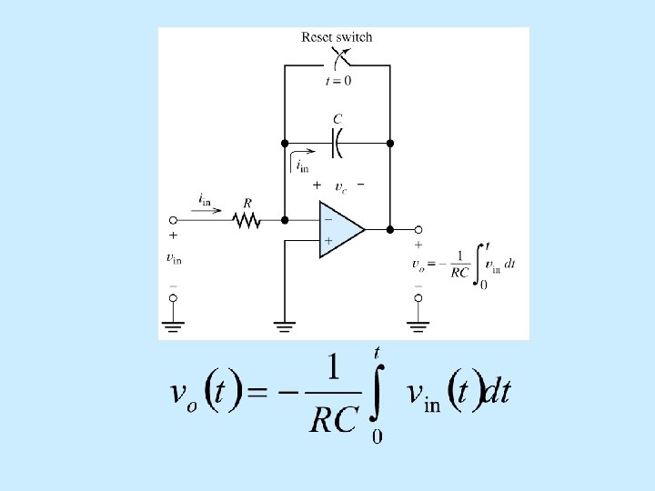
RC Op-Amp Circuits • RC operational amplifier circuits can be used to differentiate or integrate an electrical signal. • Differentiator and integrator circuits are derived from the circuit of an inverting op-amp by replacing the resistors R 1 and R 2, respectively, by a capacitor.
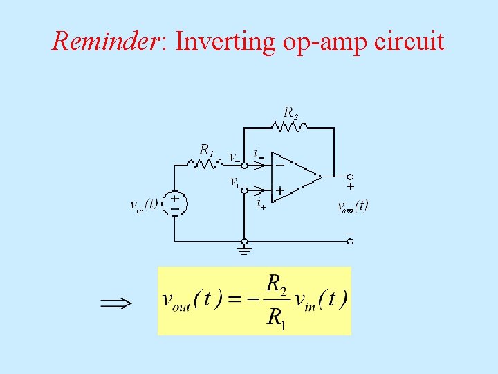
Reminder: Inverting op-amp circuit
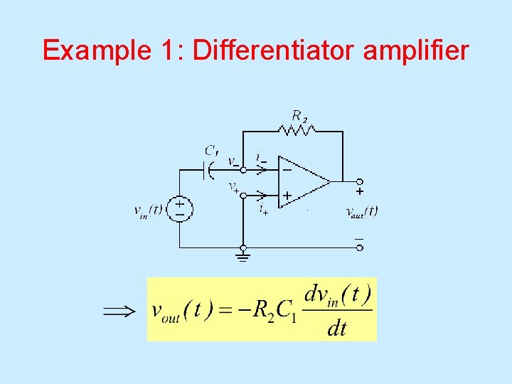
Example 1: Differentiator amplifier
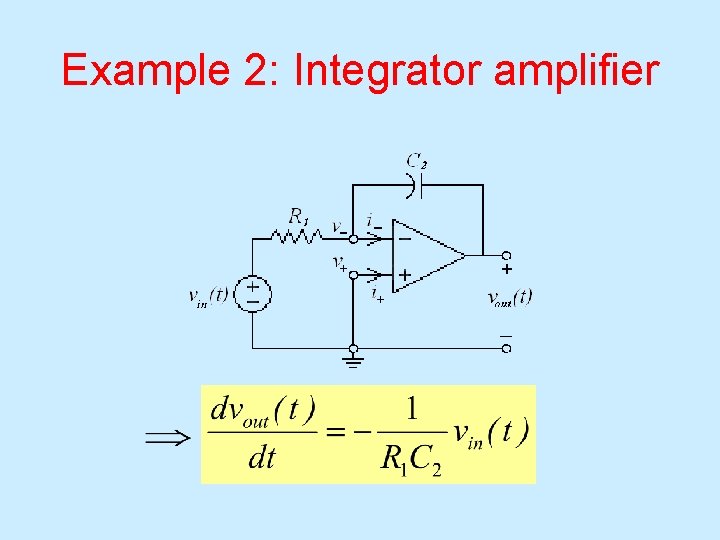
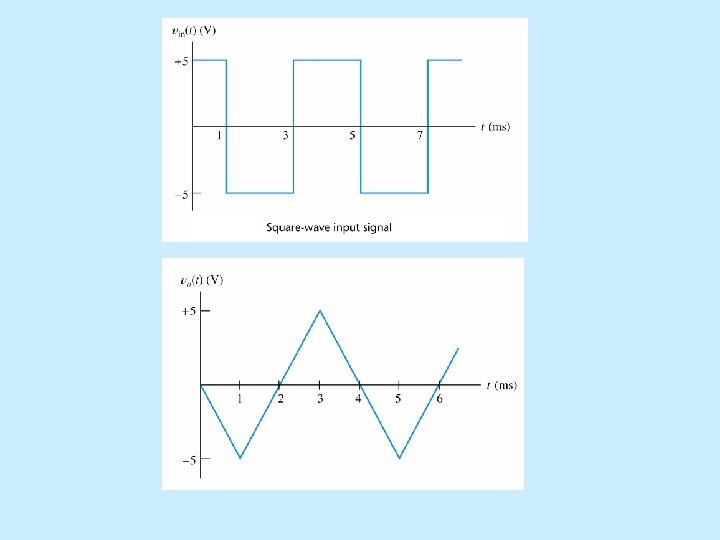
Example 2: Integrator amplifier
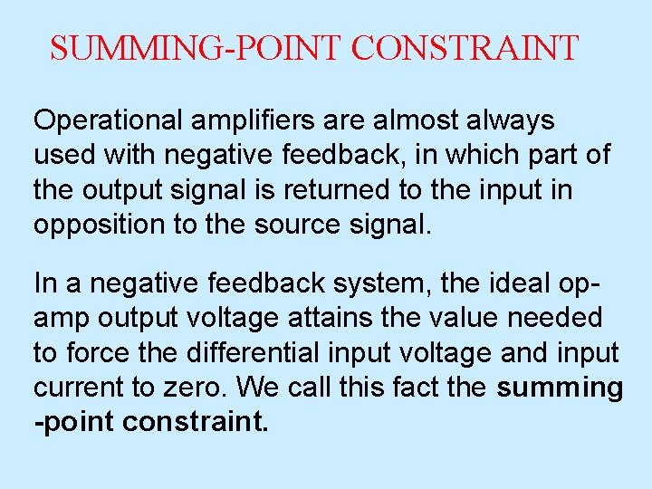
SUMMING-POINT CONSTRAINT Operational amplifiers are almost always used with negative feedback, in which part of the output signal is returned to the input in opposition to the source signal. In a negative feedback system, the ideal opamp output voltage attains the value needed to force the differential input voltage and input current to zero. We call this fact the summing -point constraint.
Golden Rules for Op-Amps • The output attempts to do whatever is necessary to make the voltage difference between the two inputs zero. (Negative Feedback is Required) • The inputs draw no current.
Ideal op-amp circuits are analyzed by the following steps: 1. Verify that negative feedback is present. 2. Assume that the differential input voltage and the input current of the op amp are forced to zero. (This is the summing-point constraint. ) 3. Apply standard circuit-analysis principles, such as Kirchhoff’s laws and Ohm’s law, to solve for the quantities of interest.
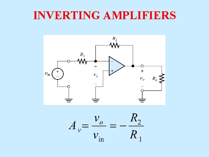
INVERTING AMPLIFIERS
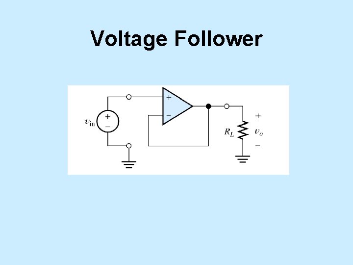
Voltage Follower
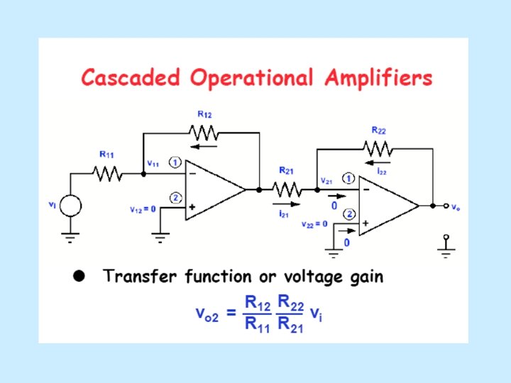
DESIGN OF SIMPLE AMPLIFIERS Amplifier design using op amps mainly consists of selecting a suitable circuit configuration and values for the feedback resistors.
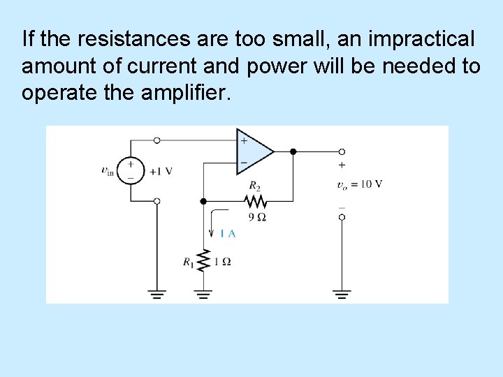
If the resistances are too small, an impractical amount of current and power will be needed to operate the amplifier.
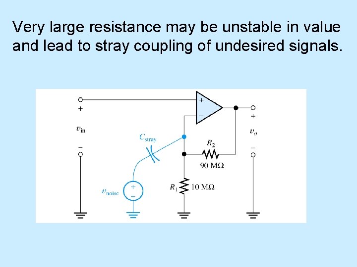
Very large resistance may be unstable in value and lead to stray coupling of undesired signals.
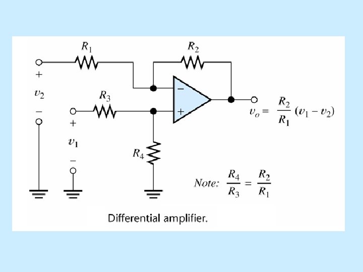
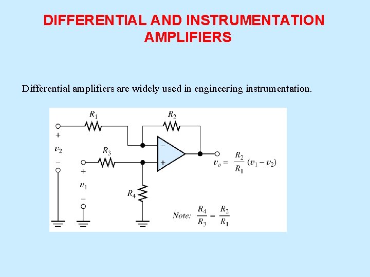
DIFFERENTIAL AND INSTRUMENTATION AMPLIFIERS Differential amplifiers are widely used in engineering instrumentation.
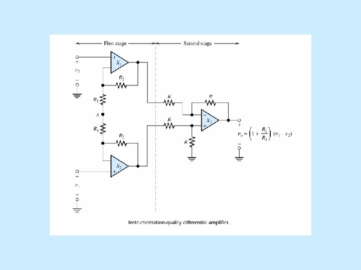
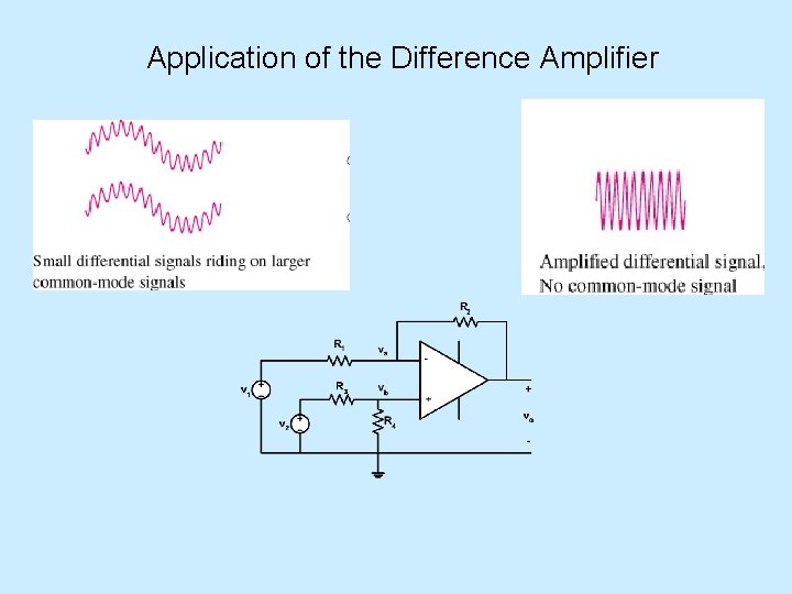
Application of the Difference Amplifier
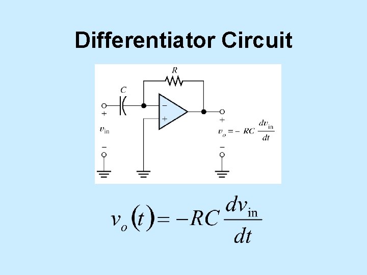
Differentiator Circuit
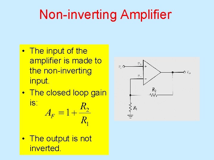
Non-inverting Amplifier • The input of the amplifier is made to the non-inverting input. • The closed loop gain is: • The output is not inverted.
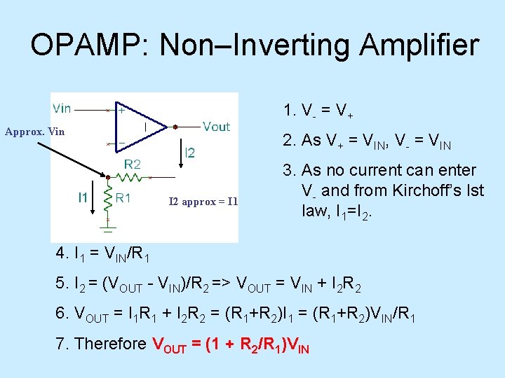
OPAMP: Non–Inverting Amplifier 1. V- = V+ Approx. Vin 2. As V+ = VIN, V- = VIN I 2 approx = I 1 3. As no current can enter V- and from Kirchoff’s Ist law, I 1=I 2. 4. I 1 = VIN/R 1 5. I 2 = (VOUT - VIN)/R 2 => VOUT = VIN + I 2 R 2 6. VOUT = I 1 R 1 + I 2 R 2 = (R 1+R 2)I 1 = (R 1+R 2)VIN/R 1 7. Therefore VOUT = (1 + R 2/R 1)VIN
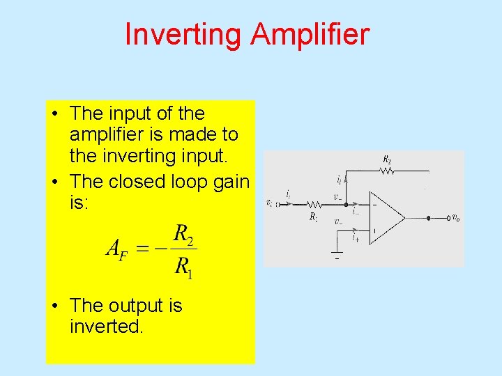
Inverting Amplifier • The input of the amplifier is made to the inverting input. • The closed loop gain is: • The output is inverted.
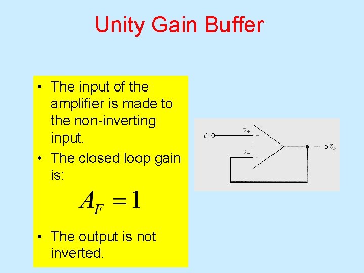
Unity Gain Buffer • The input of the amplifier is made to the non-inverting input. • The closed loop gain is: • The output is not inverted.
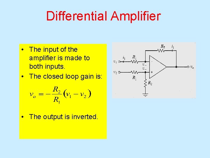
Differential Amplifier • The input of the amplifier is made to both inputs. • The closed loop gain is: • The output is inverted.
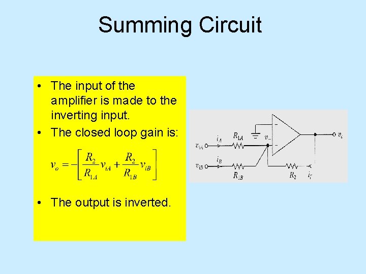
Summing Circuit • The input of the amplifier is made to the inverting input. • The closed loop gain is: • The output is inverted.
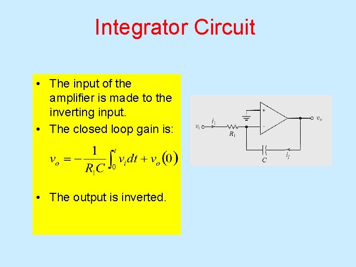
Integrator Circuit • The input of the amplifier is made to the inverting input. • The closed loop gain is: • The output is inverted.
Active Filters • Filter is a network that is frequency selective. • Passive filters uses only passive components such as: resistors, capacitors, and inductors. • Active filters uses amplifiers to achieve higher performance.
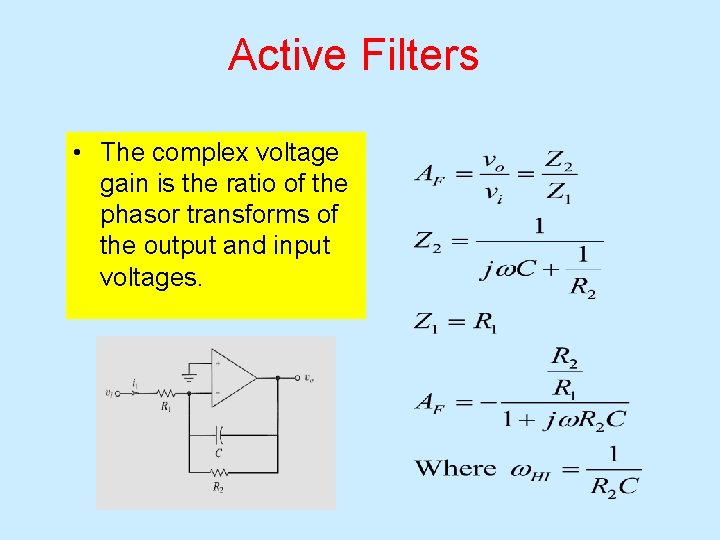
Active Filters • The complex voltage gain is the ratio of the phasor transforms of the output and input voltages.
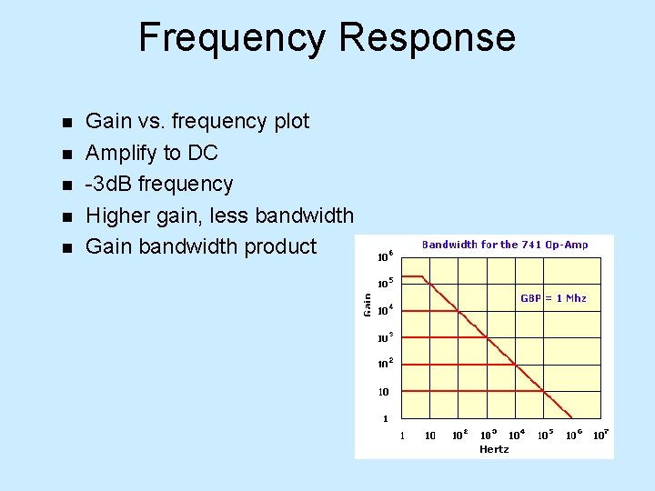
Frequency Response n n n Gain vs. frequency plot Amplify to DC -3 d. B frequency Higher gain, less bandwidth Gain bandwidth product
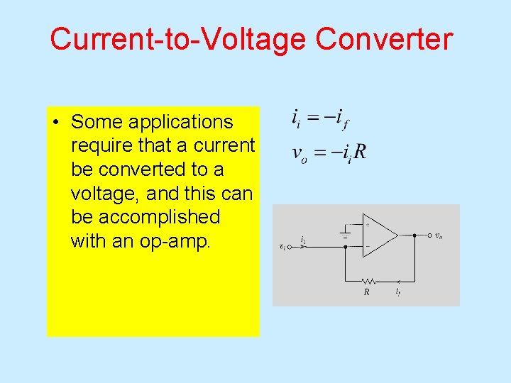
Current-to-Voltage Converter • Some applications require that a current be converted to a voltage, and this can be accomplished with an op-amp.
How are they connected in an Electric Circuit? The 741 Op Amp
The 741 Op-Amp You get all of this for around 20 cents.
Op amp application examples NONINVERTING CONFIGURATION R 2 Vin Vout Vin R 1 R 2 Vout BUFFER Vin Vout = Vin The above equations are valid only if the gain A 0 of the op amp is very high!
Voltage Output from an Amplifier Vout A Linear region Non-linear region Vin The linear range of an amplifier is finite, and limited by the supply voltage and the characteristics of the amplifier. If an amplifier is driven beyond the linear range (overdriven), overdriven serious errors can result if the gain is treated as a constant. v 0 Esat -Esat
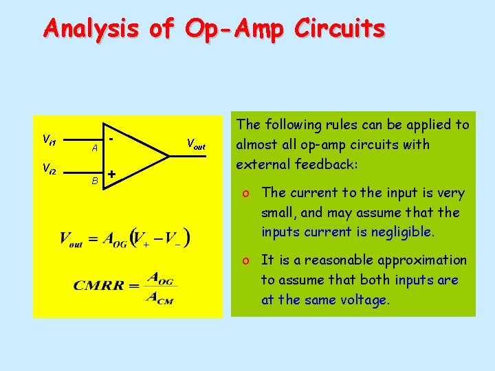
Analysis of Op-Amp Circuits Vi 1 Vi 2 A B + Vout The following rules can be applied to almost all op-amp circuits with external feedback: o The current to the input is very small, and may assume that the inputs current is negligible. o It is a reasonable approximation to assume that both inputs are at the same voltage.
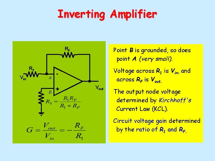
Inverting Amplifier Point B is grounded, so does point A (very small). RF R 1 Vin A B Voltage across R 1 is Vin, and across RF is Vout. + Vout The output node voltage determined by Kirchhoff's Current Law (KCL). Circuit voltage gain determined by the ratio of R 1 and RF.
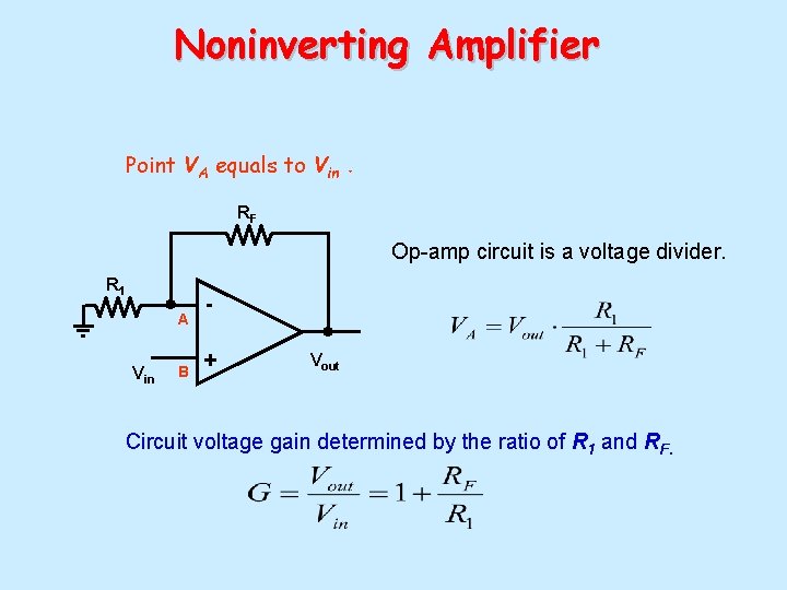
Noninverting Amplifier Point VA equals to Vin. RF Op-amp circuit is a voltage divider. R 1 A Vin B + Vout Circuit voltage gain determined by the ratio of R 1 and RF.
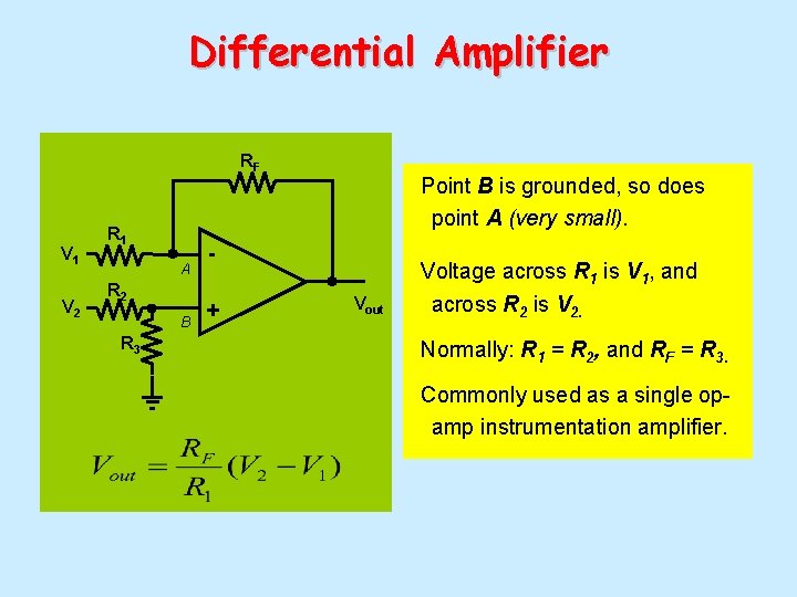
Differential Amplifier RF V 1 V 2 R 1 A R 2 B R 3 Point B is grounded, so does point A (very small). + Vout Voltage across R 1 is V 1, and across R 2 is V 2. Normally: R 1 = R 2, and RF = R 3. Commonly used as a single opamp instrumentation amplifier.



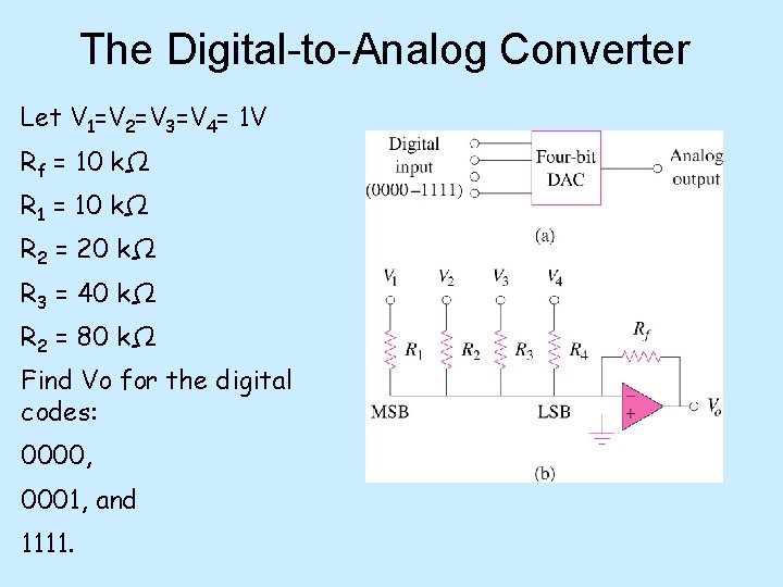
The Digital-to-Analog Converter Let V 1=V 2=V 3=V 4= 1 V Rf = 10 kΩ R 1 = 10 kΩ R 2 = 20 kΩ R 3 = 40 kΩ R 2 = 80 kΩ Find Vo for the digital codes: 0000, 0001, and 1111.
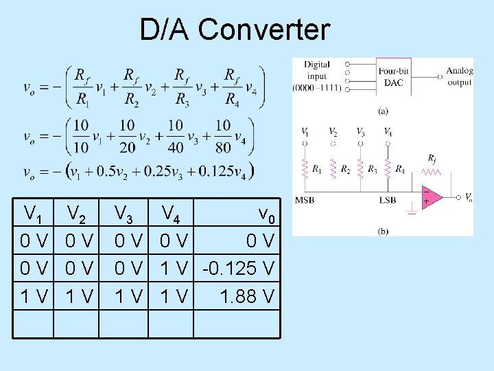
D/A Converter V 1 0 V 0 V 1 V V 2 0 V 0 V 1 V V 3 0 V 0 V 1 V V 4 v 0 0 V 0 V 1 V -0. 125 V 1 V 1. 88 V
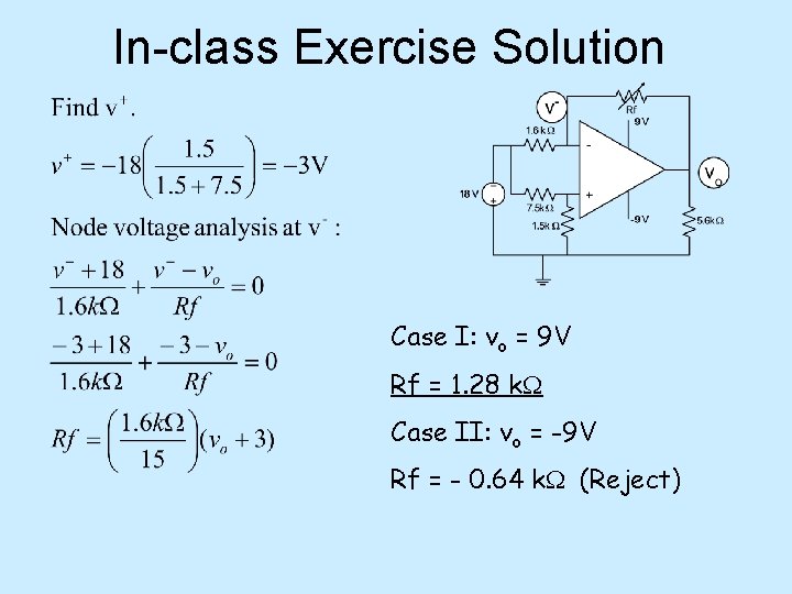
In-class Exercise Solution Case I: vo = 9 V Rf = 1. 28 k. W Case II: vo = -9 V Rf = - 0. 64 k. W (Reject)
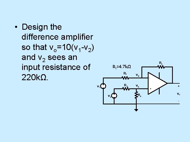
• Design the difference amplifier so that vo=10(v 1 -v 2) and v 2 sees an input resistance of 220 kΩ. R 2 R 1=4. 7 kΩ R 1 R 3 v 1 v 2 va vb R 4 + + vo -
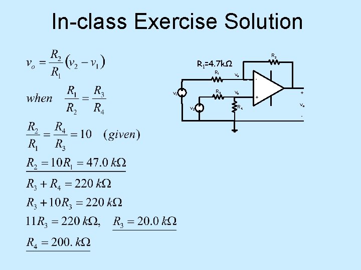
In-class Exercise Solution R 2 R 1=4. 7 kΩ R 1 R 3 v 1 v 2 va vb R 4 - + + vo -
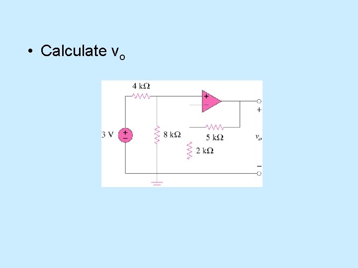
• Calculate vo
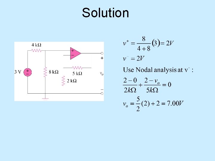
Solution
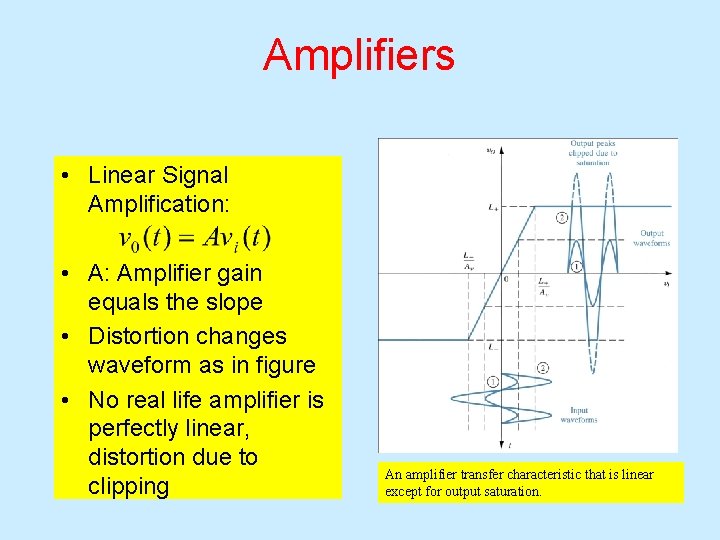
Amplifiers • Linear Signal Amplification: • A: Amplifier gain equals the slope • Distortion changes waveform as in figure • No real life amplifier is perfectly linear, distortion due to clipping An amplifier transfer characteristic that is linear except for output saturation.
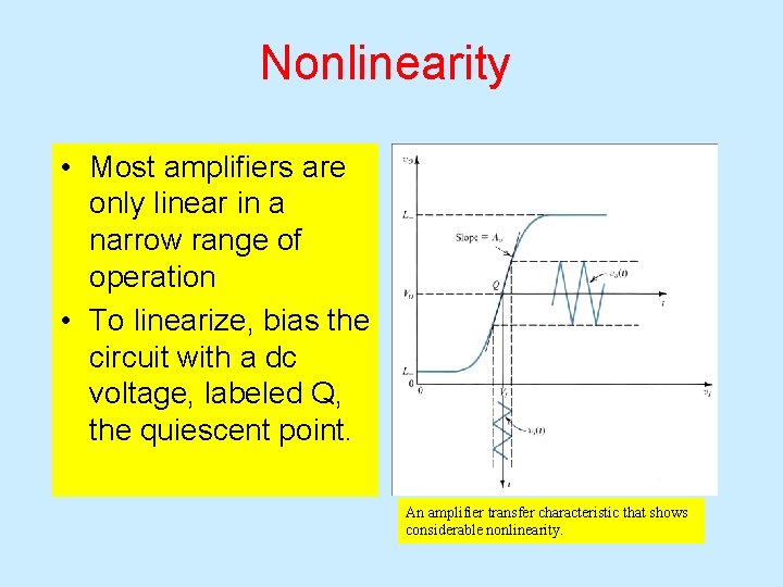
Nonlinearity • Most amplifiers are only linear in a narrow range of operation • To linearize, bias the circuit with a dc voltage, labeled Q, the quiescent point. An amplifier transfer characteristic that shows considerable nonlinearity.

Questions? Discussion? Suggestions ?

- Slides: 104