DMT 242 Wafer Fabrication Lecture 2 Semiconductor Basics

DMT 242 Wafer Fabrication Lecture 2 Semiconductor Basics

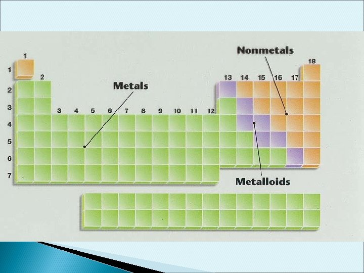
What is a semiconductor ? Ø Semiconductors are materials with electrical conductivity between conductors and insulators. Ø The most commonly used semiconductor materials are silicon, Si and germanium, Ge. Ø Some compounds, such as gallium arsenate (Ga. As), Silicon carbide (Si. C) and silicon germanium (Si. Ge). Ø Most important property is its conductivity can be controlled by adding certain impurities in the process called doping.

DMT 242 Wafer Fabrication


Devices with Different Substrates

Band Gap Atom is basic building block of all materials Classical mechanics –every atom has it own orbit structure. Electron orbits are called shells. The outermost shell is called valence shell. When electron leaves the valence shell, it becomes a free electron and can conduct electric current.

Si Pb INEE Institute of Nano Electronic Engineering 10

When 2 or more identical atoms bond together to form solid materials, their orbit overlap and form so called energy bands. Can be represented by the energy band diagram. The bottom of band is called conduction band, Ec and the top of the band is called valence, Ev. Eg = Ec –Ev Eg is defined as the energy required to break a bond in semiconductor to free an valence to conduction band leave the hole in the valence band. Electrons in conduction band are free to move and can conduct electric current. Electrons in the valence band are bonded with nuclei and cannot move freely, therefore cannot conduct electric current.

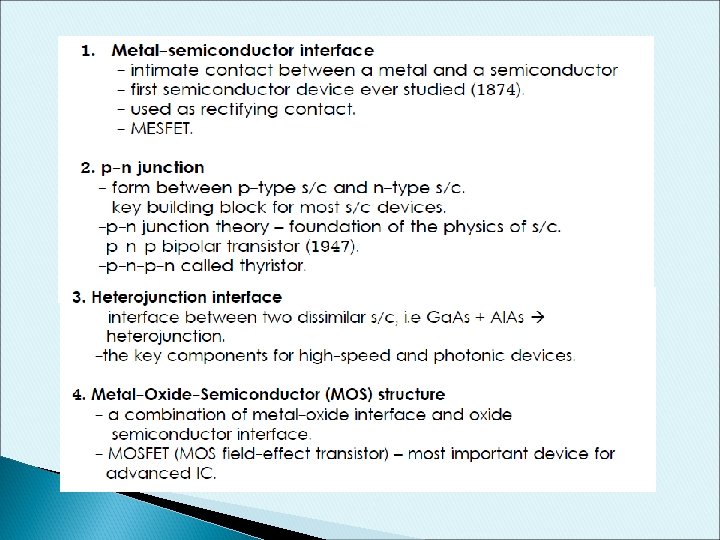
Basic Devices Building Blocks

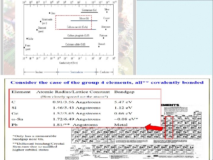
How are Silicon Wafers Specified? Resistivity • • • Resistivity is the capability of a material resisting electric current. A good conductor has a very low resistivity and a good insulator has a very high resistivity. Unit: Ohm. cm For most metals, conduction and valence bands almost overlap or very small band gap. Electron can easily jump from valence to conduction band. Therefore the conduction band has a lot of e. For insulators, the band gap is so large that electrons cannot jump across it.

Atoms Structure


Silicon wafer fabrication

Crystal Growing Silicon occurs naturally in the forms of silicon dioxide and various silicates and hence, must be purified The process of purifying silicon: ◦ Heating to produce 95% ~ 98% pure polycrystalline silicon ◦ Using Czochralski (CZ) process to grow single crystal silicon Illustration of CZ process 10 m/s 1 rev/s Liquid silicon

Crystal Growing

Czochralski Method

Wafer Slicing This step includes ◦ Slice the ingot into slices using a diamond saw ◦ Polish the surface, and ◦ Sort

DMT 242 Wafer Fabrication DOPING SEMICONDUCTOR

DMT 242 Wafer Fabrication Two types of Semiconductor Materials 1. Intrinsic Semiconductor 2. Extrinsic Semiconductor

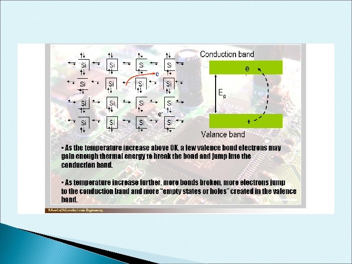
Intrinsic Semiconductor Pure semiconductor materials with no impurity atoms and no lattice defect. • At T=0 K, all energy states in valence band are filled with electrons, states in conduction band are empty. • As the temperature increase above 0 K, a few valence bond electrons may gain enough thermal energy to break the bond and jump into the conduction band. • As temperature increase further, more bonds broken, more electrons jump to the conduction band more “empty states or holes” created in the valence band. •

In intrinsic material, electrons and holes are created in pairs by thermal energy. So the number of electrons in conduction band is equal to the number of holes in the valence band • Electron concentration = hole concentration, ni= pi and nipi= ni 2 (MASS ACTION LAW) • –the product of n p is always a constant for a given semiconductor material at given temperature •


Extrinsic Semiconductor • Extrinsic s/c is defined as a semiconductor in which controlled amounts of specific dopant or impurity atoms have been added so that thermal equilibrium electron and hole concentration are different from the intrinsic carrier concentration.

Doping of Semiconductors The purpose of doping is to alter the conductivity of semiconductor materials. • Two types of dopant; p-type (B), n-type (P, As) • P-type dopants provide a hole in s/c materials, hence called acceptor. • N-type dopants provide an electron in s/c materials, hence called donors. •

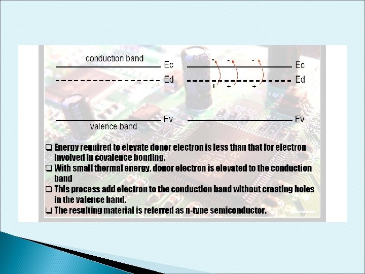
n-type Dopant • • • P and As have 5 electron valence When doped into Si, 4 electrons used to form the covalence bond with Si. 1 extra electron is left in the outermost shell and will occupy a new energy level called Donor Energy required to elevate donor electron is less than that for electron involved in covalence bonding. With small thermal energy, donor electron is elevated to the conduction band This process add electron to the conduction band without creating holes in the valence band. The resulting material is referred as n-type semiconductor. (draw the energy band atom covalent bond)


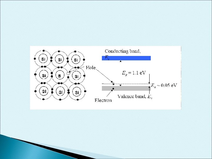
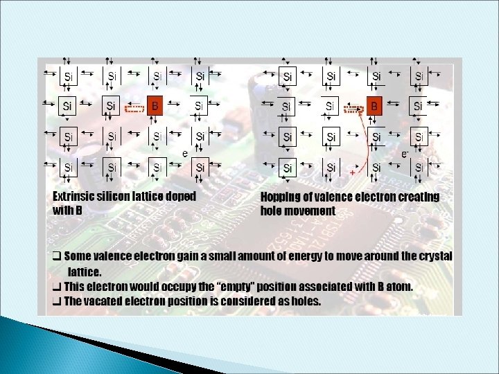
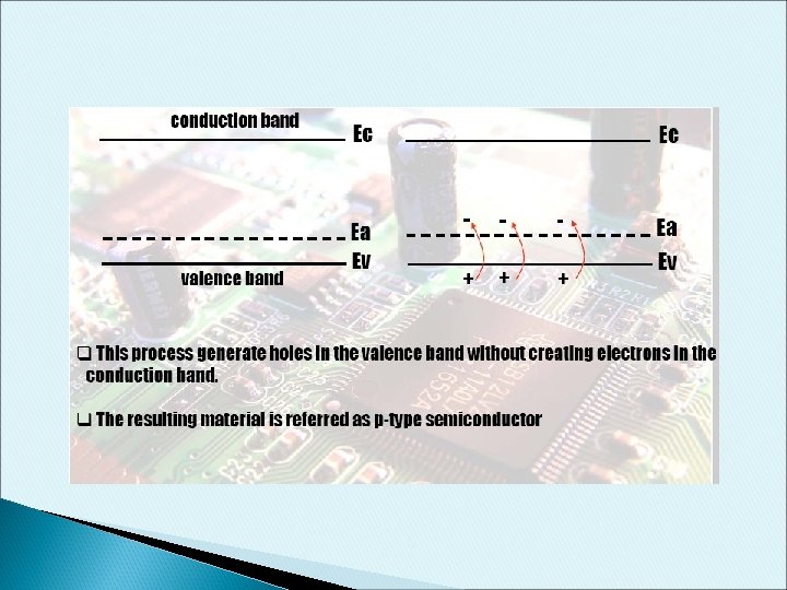
p-type Dopant • • B have 3 electron valence When doped into Si, one empty state is created in the covalence bond This empty state will occupy a new energy level called Acceptor Energy. Some valence electron gain a small amount of energy to move around the crystal lattice. This electron would occupy the “empty” position associated with B atom. The vacated electron position is considered as holes. This process generate holes in the valence band without creating electrons in the conduction band. The resulting material is referred as p-type semiconductor

Dopant Concentration and Resistivity - Pls verify this graph


• Basic Semiconductor Devices Resistor Capacitor Diode Bipolar transistor MOS transistor

Resistor The simplest electronic device. In the IC fabrication, patterned doped silicon normally used to make resistors with resistance determined by the length, line width, junction depth and dopant concentration. • Poly silicon also used a resistor. • •

Example 1 Many people use polysilicon to form gates and local interconnect. Resistivity of polysilicon is determined by dopant concentration, about 1022 cm-3, and ρ= 200 μΩ. cm. Assume polysilicon gate and local interconnect line width, height, and length are 1μm, 1μm and 100μm respectively. Calculate the resistance. ( Note: 1 um = 10 -6 m = 10 -4 cm)

Solution 1 • R = ρl / wh = 200 μΩ. cm x (100 x 10 -4) cm / [(1 x 10 -4 cm) x 1 X 10 -4 cm) = 2 x 10⁸μΩ = 200 Ω

Capacitor One of the most important IC components When two conducting materials are separated by a dielectric, a capacitor is formed. • Charge storage device • Memory devices esp. DRAM • Challenge: Reduce capacitor size while keeping the capacitance • •

DMT 242 Wafer Fabrication ε 0 -Absolute permittivity of vacuum(8. 85 x 10 -12 F/m κ-Dielectric constant


Diode • • • p-n junction Allow electric conduction only in one way (positively biased) When p-type and n-type semiconductors join together, they form a p-n junction diode. Holes in p-type region will diffuse to the n-type region, and electrons in n-type region will diffuse to the p-type region (at thermal equilibrium, without applied bias). The area dominated by minority carriers is called the transition region. The voltage across the transition region given by;

 –used extensively in high-speed circuits, analog")
Bipolar Transistor • • Bipolar junction transistor (BJT) –used extensively in high-speed circuits, analog circuits and power applications Both electrons & holes participate in the conduction process Was invented by a research team at Bell Lab in 1947 Modern bipolar transistors –replaced the germanium with Si& replaced the point contacts with two closely coupled p-n junctions in the form of p-n-p& n-p-n structures The term Bipolar is because two type of charges (electrons and holes) are involved in the flow of electricity The term Junction is because there are two p-n junctions There are two configurations for this device
 • Simple,")
MOS Transistor • Metal-oxide-semiconductor • Also called MOSFET (MOS Field Effect Transistor) • Simple, symmetric structure • Switch, good for digital, logic circuit • Most commonly used devices in the semiconductor industry NMOS Device PMOS Device

Summary of Semiconductor • Semiconductors have the conductivity between conductors and insulators • Semiconductor conductivity can be controlled by dopant concentration: the higher the dopant concentration, the lower the semiconductor’s resistivity • Holes form the majority of carriers in p-type semiconductors. Boron is a p-type dopant. • The majority of carriers in n-type semiconductors are electrons. Phosporous, arsenic and antimony are n-type dopants. • At the same dopant concentration and temperature, n-type semiconductors have lower resistivity than p-type semiconductors because of the higher mobility of electrons compared to holes. INEE Institute of Nano Electronic Engineering 53

Summary INEE Institute of Nano Electronic Engineering 54

Summary INEE Institute of Nano Electronic Engineering 55

DMT 242 Wafer Fabrication Q &A
- Slides: 56