
DMT 234 Semiconductor Physics Device LECTURE 8 METAL


- Slides: 53
DMT 234 Semiconductor Physics & Device LECTURE 8 METAL OXIDE SEMICONDUCTOR FIELD EFFECT TRANSISTOR (MOSFET)
DMT 234 SEMICONDUCTOR PHYSICS & DEVICE Preview q The material in this chapter presumes a knowledge only on the semiconductor material properties and characterisitics of the pn junction. q MOSFET in the conjunction with other circuit element, is capable of voltage gain and power signal gain. q Used extensively in digital circuit application where, because of its relatively small size, thousands of devices can be fabricated in a single integrated circuit. q Implicity used only for the metal-silicon dioxide – silicon system. q The heart of the MOSFET is known as MOS capacitor and Diode.
DMT 234 Semiconductor Physic & Device 8. 1 MOS Capacitor Ø The heart of MOSFET is a metal-oxide-semiconductor structure known as an MOS capacitor. Ø The energy bands in the semiconductor near the oxide-semiconductor interface bends as a voltage is applied across MOS capacitor. Ø The position of the conduction and valence bands is relatively dependence on MOS capacitor voltage. Ø So the characteristics semiconductor surface can be inverted from ptype to n-type, or in mirror condition by applying proper voltage. Ø The operation and characteristics of MOSFET are dependent on this inversion and the creation an inversion charge density at the semiconductor surface. Ø The threshold voltage is defined as the applied gate voltage require to create the inversion layer charge and is one of the important parameters of the MOSFET.
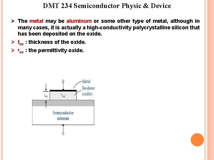
DMT 234 Semiconductor Physic & Device Ø The metal may be aluminum or some other type of metal, although in many cases, it is actually a high-conductivity polycrystalline silicon that has been deposited on the oxide. Ø tox : thickness of the oxide. Ø ᵋox : the permittivity oxide.
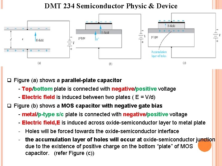
DMT 234 Semiconductor Physic & Device q Figure (a) shows a parallel-plate capacitor - Top/bottom plate is connected with negative/positive voltage - Electric field is induced between two plates ( E = V/d) q Figure (b) shows a MOS capacitor with negative gate bias - metal/p-type s/c plate is connected with negative/positive voltage - Electric field, E is induced across oxide-semiconductor layer to metal plate - Holes will be forced towards the oxide-semiconductor interface - the accumulation layer of holes will occur at oxide-semiconductor junction due to the existence of positive charge on the bottom “plate” of MOS capacitor. (refer Figure (c))
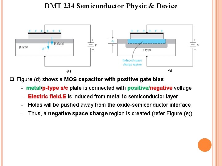
DMT 234 Semiconductor Physic & Device (d) (e) q Figure (d) shows a MOS capacitor with positive gate bias - metal/p-type s/c plate is connected with positive/negative voltage - Electric field, E is induced from metal to semiconductor layer - Holes will be pushed away from the oxide-semiconductor interface - Thus, a negative space charge region is created (refer Figure (e))
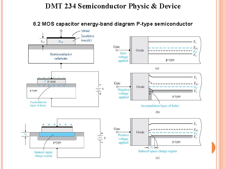
DMT 234 Semiconductor Physic & Device 8. 2 MOS capacitor energy-band diagram P-type semiconductor
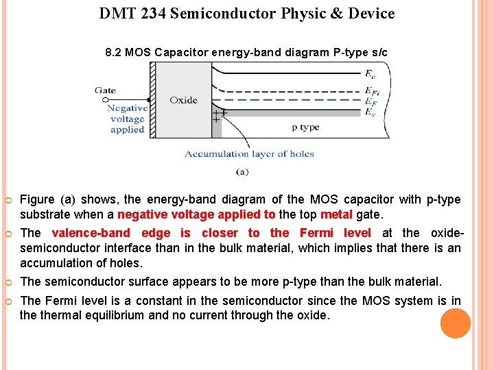
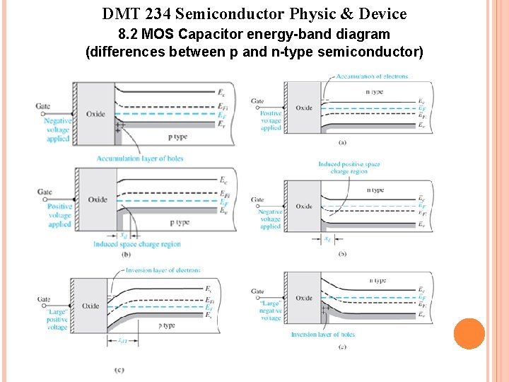
DMT 234 Semiconductor Physic & Device 8. 2 MOS Capacitor energy-band diagram P-type s/c Figure (a) shows, the energy-band diagram of the MOS capacitor with p-type substrate when a negative voltage applied to the top metal gate. The valence-band edge is closer to the Fermi level at the oxidesemiconductor interface than in the bulk material, which implies that there is an accumulation of holes. The semiconductor surface appears to be more p-type than the bulk material. The Fermi level is a constant in the semiconductor since the MOS system is in thermal equilibrium and no current through the oxide.
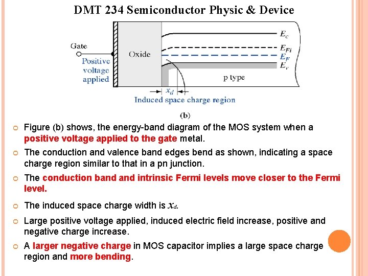
DMT 234 Semiconductor Physic & Device Figure (b) shows, the energy-band diagram of the MOS system when a positive voltage applied to the gate metal. The conduction and valence band edges bend as shown, indicating a space charge region similar to that in a pn junction. The conduction band intrinsic Fermi levels move closer to the Fermi level. The induced space charge width is xd. Large positive voltage applied, induced electric field increase, positive and negative charge increase. A larger negative charge in MOS capacitor implies a large space charge region and more bending.
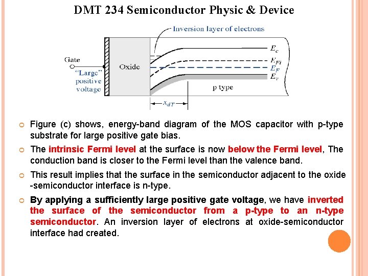
DMT 234 Semiconductor Physic & Device Figure (c) shows, energy-band diagram of the MOS capacitor with p-type substrate for large positive gate bias. The intrinsic Fermi level at the surface is now below the Fermi level, The conduction band is closer to the Fermi level than the valence band. This result implies that the surface in the semiconductor adjacent to the oxide -semiconductor interface is n-type. By applying a sufficiently large positive gate voltage, we have inverted the surface of the semiconductor from a p-type to an n-type semiconductor. An inversion layer of electrons at oxide-semiconductor interface had created.
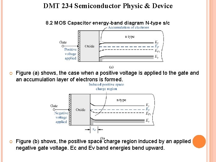
DMT 234 Semiconductor Physic & Device 8. 2 MOS Capacitor energy-band diagram N-type s/c Figure (a) shows, the case when a positive voltage is applied to the gate and an accumulation layer of electrons is formed. Figure (b) shows, the positive space charge region induced by an applied negative gate voltage. Ec and Ev band energies bend upward.
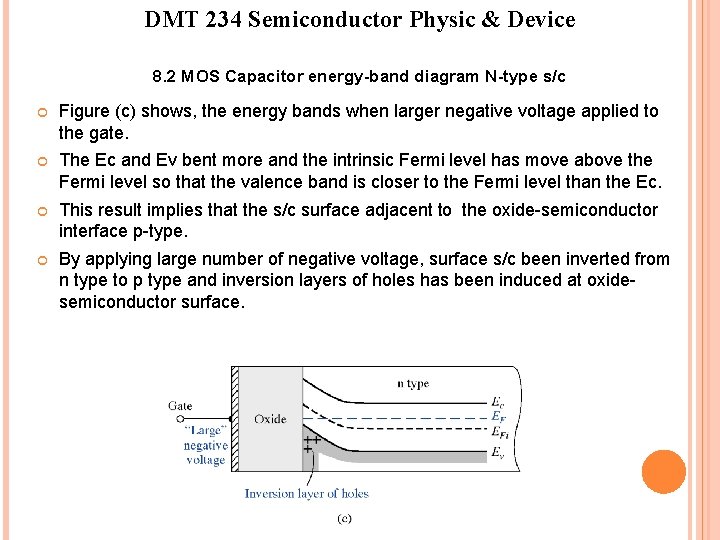
DMT 234 Semiconductor Physic & Device 8. 2 MOS Capacitor energy-band diagram N-type s/c Figure (c) shows, the energy bands when larger negative voltage applied to the gate. The Ec and Ev bent more and the intrinsic Fermi level has move above the Fermi level so that the valence band is closer to the Fermi level than the Ec. This result implies that the s/c surface adjacent to the oxide-semiconductor interface p-type. By applying large number of negative voltage, surface s/c been inverted from n type to p type and inversion layers of holes has been induced at oxidesemiconductor surface.
DMT 234 Semiconductor Physic & Device 8. 2 MOS Capacitor energy-band diagram (differences between p and n-type semiconductor)
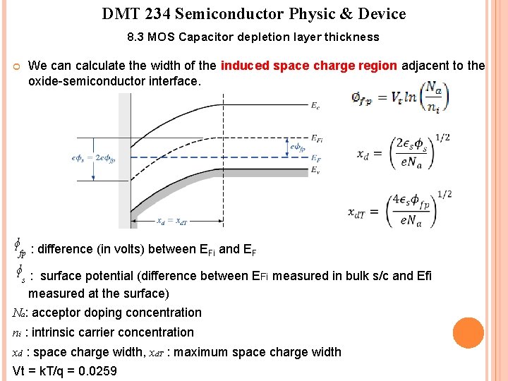
DMT 234 Semiconductor Physic & Device 8. 3 MOS Capacitor depletion layer thickness We can calculate the width of the induced space charge region adjacent to the oxide-semiconductor interface. ᶲ ᶲ fp : difference (in volts) between EFi and EF s : surface potential (difference between EFi measured in bulk s/c and Efi measured at the surface) Na: acceptor doping concentration ni : intrinsic carrier concentration xd : space charge width, xd. T : maximum space charge width Vt = k. T/q = 0. 0259
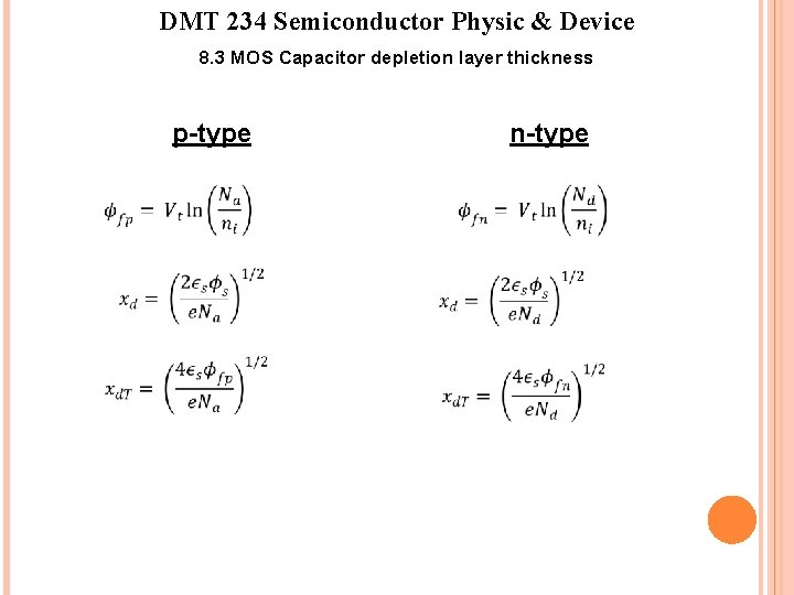
DMT 234 Semiconductor Physic & Device 8. 3 MOS Capacitor depletion layer thickness p-type n-type
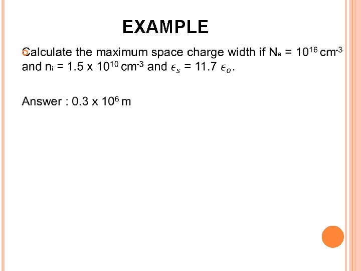
EXAMPLE
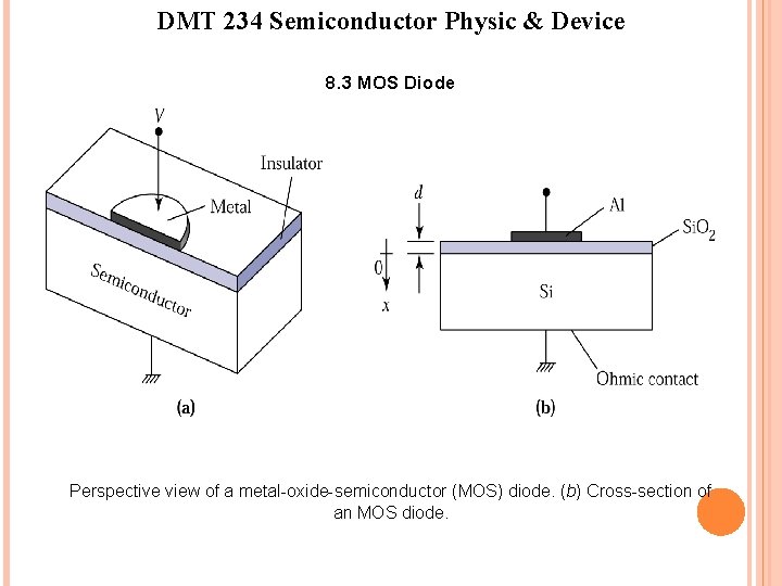
DMT 234 Semiconductor Physic & Device 8. 3 MOS Diode Perspective view of a metal-oxide-semiconductor (MOS) diode. (b) Cross-section of an MOS diode.
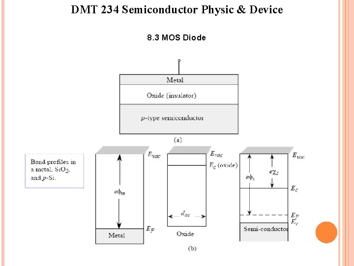
DMT 234 Semiconductor Physic & Device 8. 3 MOS Diode
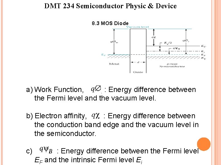
DMT 234 Semiconductor Physic & Device 8. 3 MOS Diode a) Work Function, : Energy difference between the Fermi level and the vacuum level. b) Electron affinity, : Energy difference between the conduction band edge and the vacuum level in the semiconductor. c) : Energy difference between the Fermi level EF and the intrinsic Fermi level Ei
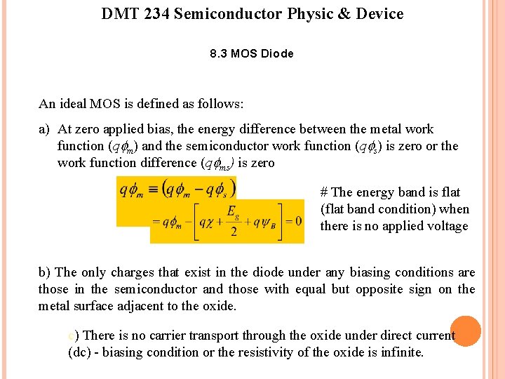
DMT 234 Semiconductor Physic & Device 8. 3 MOS Diode An ideal MOS is defined as follows: a) At zero applied bias, the energy difference between the metal work function (q m) and the semiconductor work function (q s) is zero or the work function difference (q ms) is zero # The energy band is flat (flat band condition) when there is no applied voltage b) The only charges that exist in the diode under any biasing conditions are those in the semiconductor and those with equal but opposite sign on the metal surface adjacent to the oxide. c) There is no carrier transport through the oxide under direct current (dc) - biasing condition or the resistivity of the oxide is infinite.
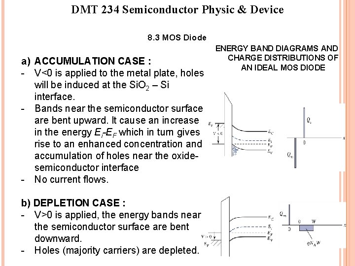
DMT 234 Semiconductor Physic & Device 8. 3 MOS Diode a) ACCUMULATION CASE : - V<0 is applied to the metal plate, holes will be induced at the Si. O 2 – Si interface. - Bands near the semiconductor surface are bent upward. It cause an increase in the energy Ei-EF which in turn gives rise to an enhanced concentration and accumulation of holes near the oxidesemiconductor interface - No current flows. b) DEPLETION CASE : - V>0 is applied, the energy bands near the semiconductor surface are bent downward. - Holes (majority carriers) are depleted. ENERGY BAND DIAGRAMS AND CHARGE DISTRIBUTIONS OF AN IDEAL MOS DIODE
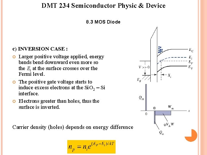
DMT 234 Semiconductor Physic & Device 8. 3 MOS Diode c) INVERSION CASE : Larger positive voltage applied, energy bands bend downward even more so the Ei at the surface crosses over the Fermi level. The positive gate voltage starts to induce excess electrons at the Si. O 2 – Si interface. Electrons greater than holes, thus the surface is inverted. Carrier density (holes) depends on energy difference
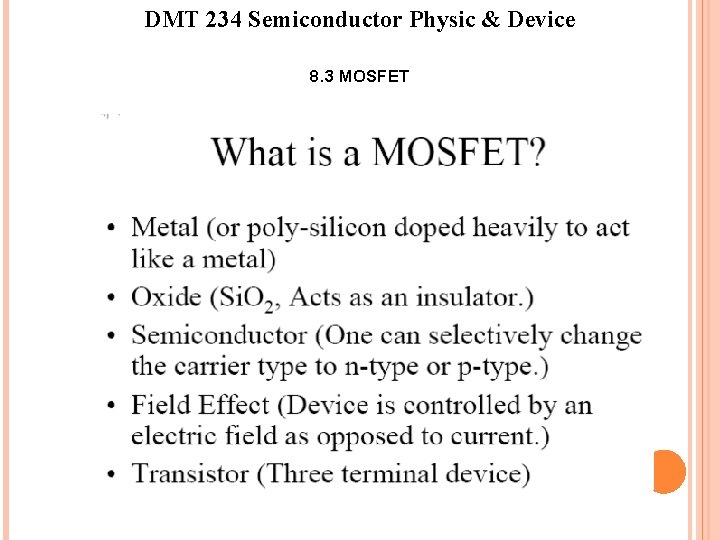
DMT 234 Semiconductor Physic & Device 8. 3 MOSFET
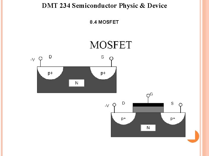
DMT 234 Semiconductor Physic & Device 8. 4 MOSFET
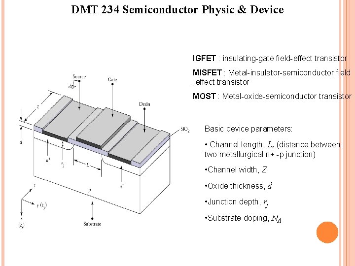
DMT 234 Semiconductor Physic & Device IGFET : insulating-gate field-effect transistor MISFET : Metal-insulator-semiconductor field -effect transistor MOST : Metal-oxide-semiconductor transistor Basic device parameters: • Channel length, L, (distance between two metallurgical n+ -p junction) • Channel width, Z • Oxide thickness, d • Junction depth, rj • Substrate doping, NA
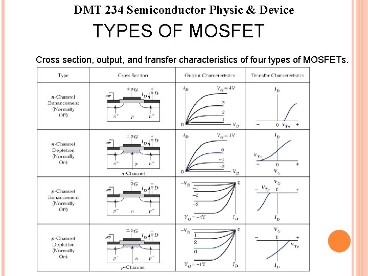
DMT 234 Semiconductor Physic & Device TYPES OF MOSFET Cross section, output, and transfer characteristics of four types of MOSFETs.
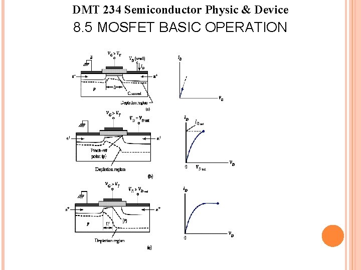
DMT 234 Semiconductor Physic & Device 8. 5 MOSFET BASIC OPERATION
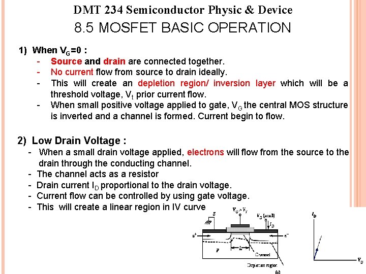
DMT 234 Semiconductor Physic & Device 8. 5 MOSFET BASIC OPERATION 1) When VG=0 : - Source and drain are connected together. - No current flow from source to drain ideally. - This will create an depletion region/ inversion layer which will be a threshold voltage, Vt prior current flow. - When small positive voltage applied to gate, VG the central MOS structure is inverted and a channel is formed. Current begin to flow. 2) Low Drain Voltage : - When a small drain voltage applied, electrons will flow from the source to the drain through the conducting channel. - The channel acts as a resistor - Drain current ID proportional to the drain voltage. - Current flow can be controlled by using gate voltage. - This will create a linear region in IV curve
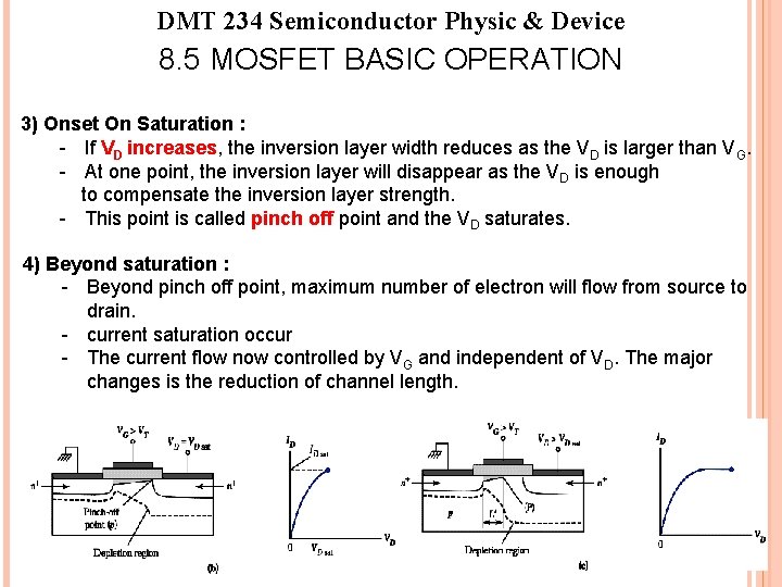
DMT 234 Semiconductor Physic & Device 8. 5 MOSFET BASIC OPERATION 3) Onset On Saturation : - If VD increases, the inversion layer width reduces as the VD is larger than VG. - At one point, the inversion layer will disappear as the VD is enough to compensate the inversion layer strength. - This point is called pinch off point and the VD saturates. 4) Beyond saturation : - Beyond pinch off point, maximum number of electron will flow from source to drain. - current saturation occur - The current flow now controlled by VG and independent of VD. The major changes is the reduction of channel length.
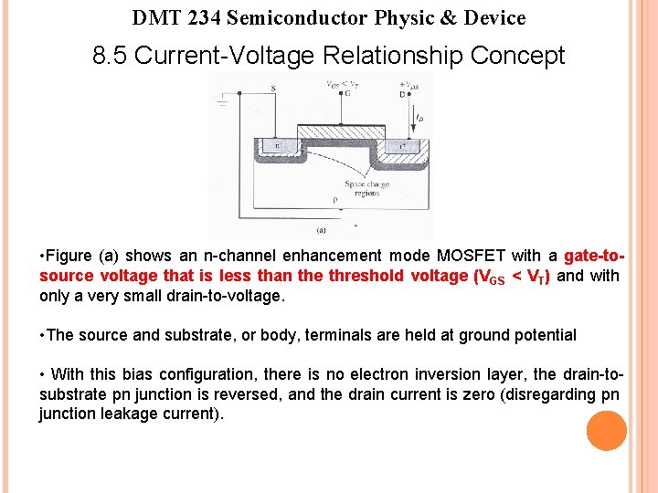
DMT 234 Semiconductor Physic & Device 8. 5 Current-Voltage Relationship Concept • Figure (a) shows an n-channel enhancement mode MOSFET with a gate-tosource voltage that is less than the threshold voltage (VGS < VT) and with only a very small drain-to-voltage. • The source and substrate, or body, terminals are held at ground potential • With this bias configuration, there is no electron inversion layer, the drain-tosubstrate pn junction is reversed, and the drain current is zero (disregarding pn junction leakage current).
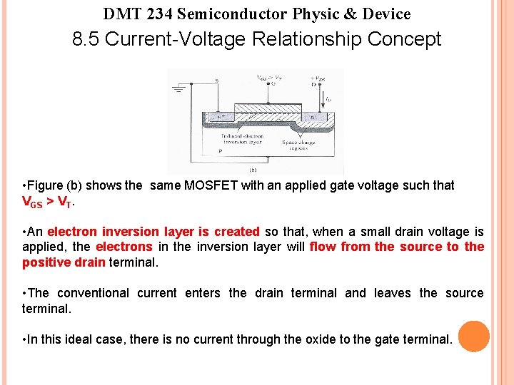
DMT 234 Semiconductor Physic & Device 8. 5 Current-Voltage Relationship Concept • Figure (b) shows the same MOSFET with an applied gate voltage such that VGS > VT. • An electron inversion layer is created so that, when a small drain voltage is applied, the electrons in the inversion layer will flow from the source to the positive drain terminal. • The conventional current enters the drain terminal and leaves the source terminal. • In this ideal case, there is no current through the oxide to the gate terminal.
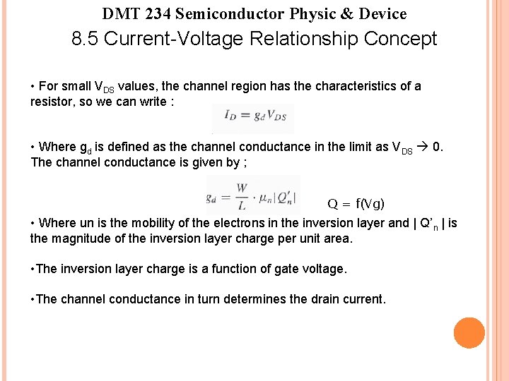
DMT 234 Semiconductor Physic & Device 8. 5 Current-Voltage Relationship Concept • For small VDS values, the channel region has the characteristics of a resistor, so we can write : • Where gd is defined as the channel conductance in the limit as VDS 0. The channel conductance is given by ; Q = f(Vg) • Where un is the mobility of the electrons in the inversion layer and | Q’n | is the magnitude of the inversion layer charge per unit area. • The inversion layer charge is a function of gate voltage. • The channel conductance in turn determines the drain current.
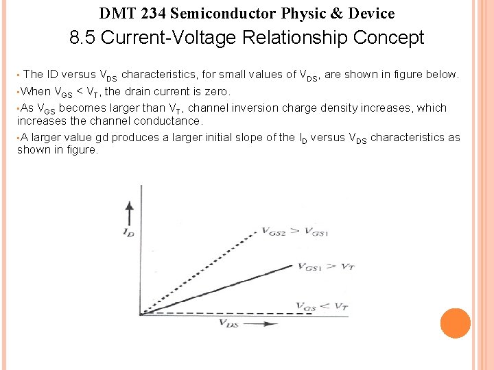
DMT 234 Semiconductor Physic & Device 8. 5 Current-Voltage Relationship Concept The ID versus VDS characteristics, for small values of VDS, are shown in figure below. • When VGS < VT, the drain current is zero. • As VGS becomes larger than VT, channel inversion charge density increases, which increases the channel conductance. • A larger value gd produces a larger initial slope of the ID versus VDS characteristics as shown in figure. •
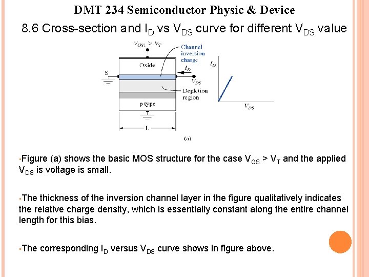
DMT 234 Semiconductor Physic & Device 8. 6 Cross-section and ID vs VDS curve for different VDS value • Figure (a) shows the basic MOS structure for the case VGS > VT and the applied VDS is voltage is small. • The thickness of the inversion channel layer in the figure qualitatively indicates the relative charge density, which is essentially constant along the entire channel length for this bias. • The corresponding ID versus VDS curve shows in figure above.
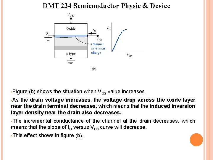
DMT 234 Semiconductor Physic & Device • Figure (b) shows the situation when VDS value increases. • As the drain voltage increases, the voltage drop across the oxide layer near the drain terminal decreases, which means that the induced inversion layer density near the drain also decreases. • The incremental conductance of the channel at the drain decreases, which means that the slope of ID versus VDS curve will decrease. • This effect shows in figure (b).
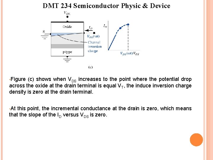
DMT 234 Semiconductor Physic & Device • Figure (c) shows when VDS increases to the point where the potential drop across the oxide at the drain terminal is equal VT, the induce inversion charge density is zero at the drain terminal. • At this point, the incremental conductance at the drain is zero, which means that the slope of the ID versus VDS is zero.
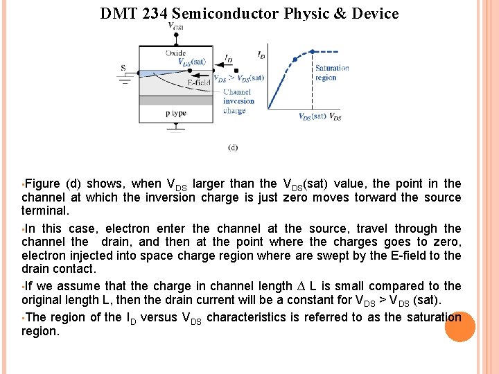
DMT 234 Semiconductor Physic & Device • Figure (d) shows, when VDS larger than the VDS(sat) value, the point in the channel at which the inversion charge is just zero moves torward the source terminal. • In this case, electron enter the channel at the source, travel through the channel the drain, and then at the point where the charges goes to zero, electron injected into space charge region where are swept by the E-field to the drain contact. • If we assume that the charge in channel length ∆ L is small compared to the original length L, then the drain current will be a constant for VDS > VDS (sat). • The region of the ID versus VDS characteristics is referred to as the saturation region.
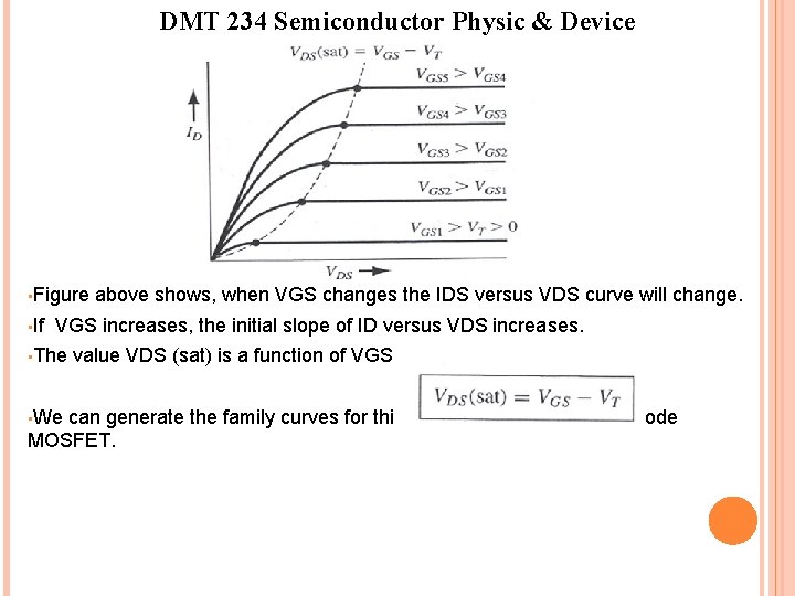
DMT 234 Semiconductor Physic & Device • Figure • If above shows, when VGS changes the IDS versus VDS curve will change. VGS increases, the initial slope of ID versus VDS increases. • The • We value VDS (sat) is a function of VGS. can generate the family curves for this n-channel enhancement mode MOSFET.
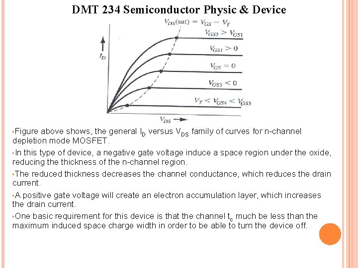
DMT 234 Semiconductor Physic & Device • Figure above shows, the general ID versus VDS family of curves for n-channel depletion mode MOSFET. • In this type of device, a negative gate voltage induce a space region under the oxide, reducing the thickness of the n-channel region. • The reduced thickness decreases the channel conductance, which reduces the drain current. • A positive gate voltage will create an electron accumulation layer, which increases the drain current. • One basic requirement for this device is that the channel tc much be less than the maximum induced space charge width in order to be able to turn the device off.
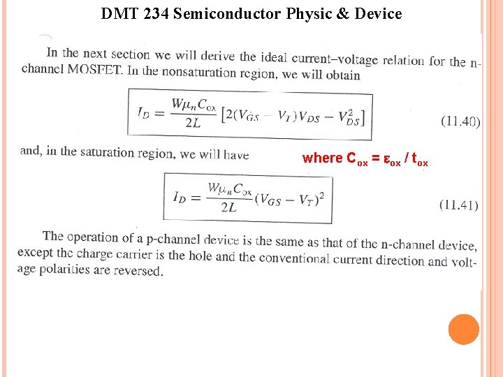
DMT 234 Semiconductor Physic & Device where Cox = ox / tox
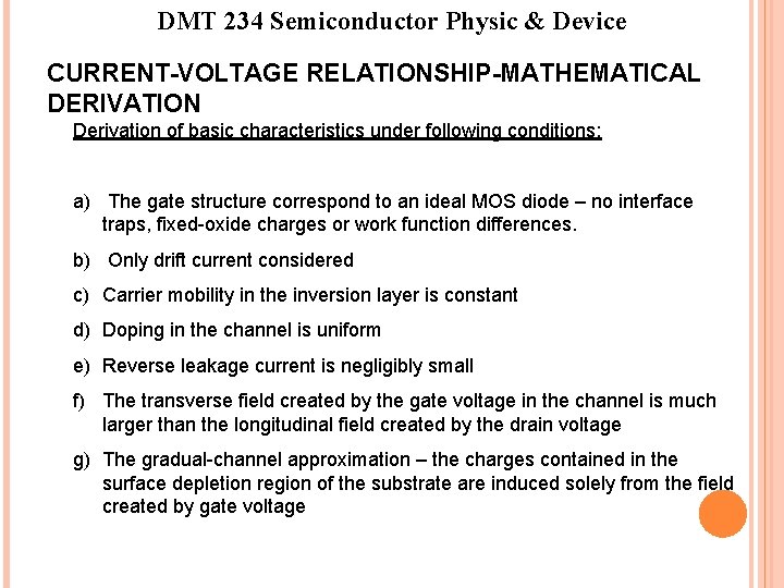
DMT 234 Semiconductor Physic & Device CURRENT-VOLTAGE RELATIONSHIP-MATHEMATICAL DERIVATION Derivation of basic characteristics under following conditions: a) The gate structure correspond to an ideal MOS diode – no interface traps, fixed-oxide charges or work function differences. b) Only drift current considered c) Carrier mobility in the inversion layer is constant d) Doping in the channel is uniform e) Reverse leakage current is negligibly small f) The transverse field created by the gate voltage in the channel is much larger than the longitudinal field created by the drain voltage g) The gradual-channel approximation – the charges contained in the surface depletion region of the substrate are induced solely from the field created by gate voltage
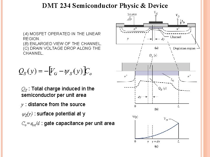
DMT 234 Semiconductor Physic & Device (A) MOSFET OPERATED IN THE LINEAR REGION. (B) ENLARGED VIEW OF THE CHANNEL. (C) DRAIN VOLTAGE DROP ALONG THE CHANNEL. QS : Total charge induced in the semiconductor per unit area y : distance from the source S(y) : surface potential at y Co= ox/d : gate capacitance per unit area
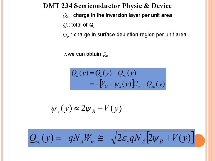
DMT 234 Semiconductor Physic & Device Qn : charge in the inversion layer per unit area Qs: total of Qn Qsc : charge in surface depletion region per unit area we can obtain Qn
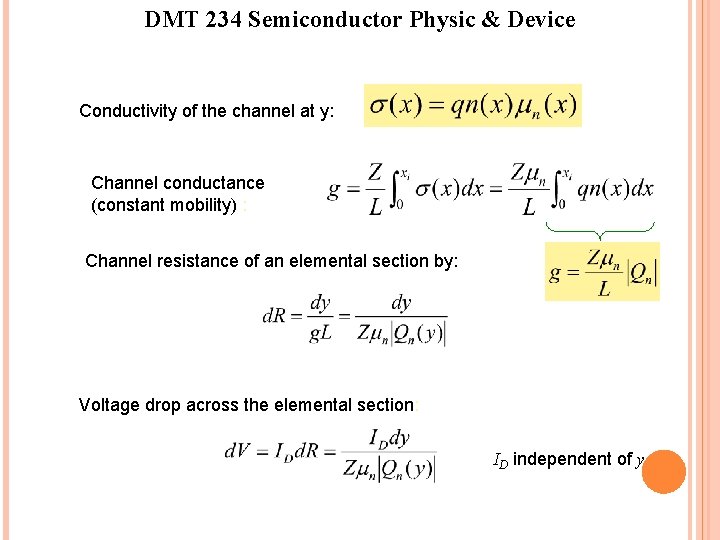
DMT 234 Semiconductor Physic & Device Conductivity of the channel at y: Channel conductance (constant mobility) : Channel resistance of an elemental section by: Voltage drop across the elemental section: ID independent of y
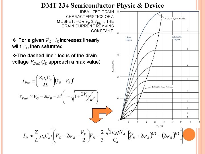
DMT 234 Semiconductor Physic & Device IDEALIZED DRAIN CHARACTERISTICS OF A MOSFET. FOR VD VDSAT, THE DRAIN CURRENT REMAINS CONSTANT. v For a given VG : ID increases linearly with VD then saturated v. The dashed line : locus of the drain voltage VDsat (ID approach a max value)
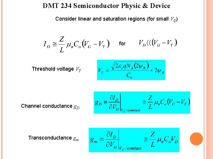
DMT 234 Semiconductor Physic & Device Consider linear and saturation regions (for small VD) for Threshold voltage VT : Channel conductance g. D : Transconductance gm :
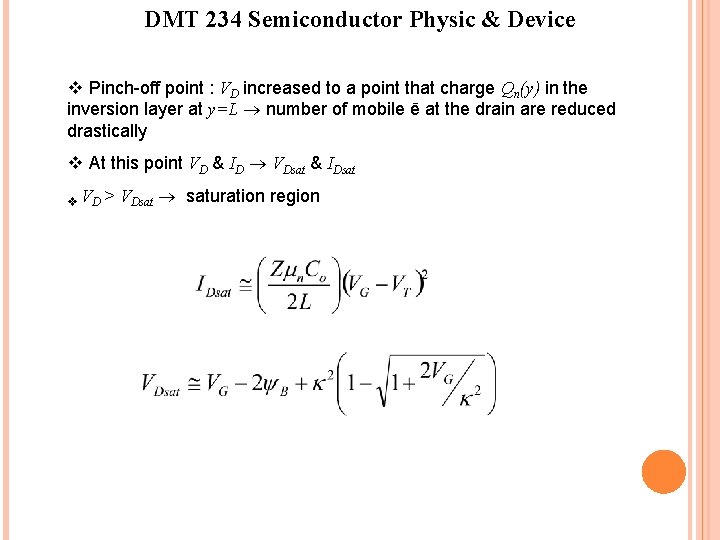
DMT 234 Semiconductor Physic & Device v Pinch-off point : VD increased to a point that charge Qn(y) in the inversion layer at y=L number of mobile ē at the drain are reduced drastically v At this point VD & ID VDsat & IDsat v VD > VDsat saturation region
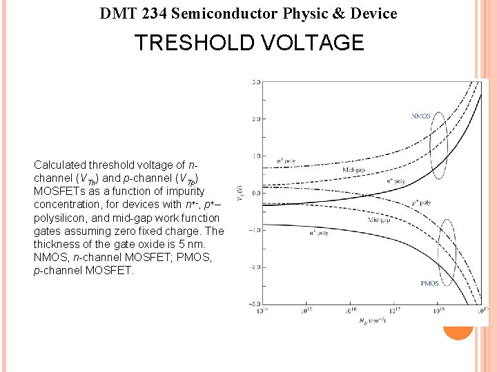
DMT 234 Semiconductor Physic & Device TRESHOLD VOLTAGE Calculated threshold voltage of nchannel (VTn) and p-channel (VTp) MOSFETs as a function of impurity concentration, for devices with n+-, p+– polysilicon, and mid-gap work function gates assuming zero fixed charge. The thickness of the gate oxide is 5 nm. NMOS, n-channel MOSFET; PMOS, p-channel MOSFET.
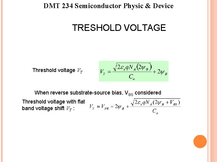
DMT 234 Semiconductor Physic & Device TRESHOLD VOLTAGE Threshold voltage VT : When reverse substrate-source bias, VBS considered Threshold voltage with flat band voltage shift VT :
DMT 234 Semiconductor Physic & Device MOSFET APPLICATION ¡ MOSFET applied in the semiconductor industry for : a) VLSI Circuits b) Memory Devices ( DRAM, SRAM, Nonvolatile Memory) c) CMOS Digital Circuit d) Microprocessors Advantages of MOSFET : a) In CMOS, perfect zero current when input switch off. Good logic ‘ 1’ and logic ‘ 0’ condition. b) Ability to scale down in size. (Channel length, width, area) c) Ability to control threshold voltage when device shrink. Quick switching. d) Oxide layer between gate and channel prevent DC flow – Power Consumption. e) Low power consumption allow more components per chip surface area.
DMT 234 Semiconductor Physic & Device DISADVANTAGES OF MOSFET Reduces VT makes MOSFET could not switched off – weak inversion layer. Interconnect capacitance between wires – device miniature reduces. Heat production impact – shrink device size, increasing device quantity. Thin oxide requirement – gate oxide tunneling leakage problem. Increased process fabrication steps – complex circuit design.
DMT 234 Semiconductor Physic & Device GOOD LUCK FOR FINAL EXAM!!
DMT 234 Semiconductor Physic & Device Next Topic : Tutorial & Clinic review