DMT 231 3 ANALOGUE ELECTRONICS Lecture I Multistage
- Slides: 57

DMT 231 / 3 ANALOGUE ELECTRONICS Lecture I Multistage Amplifiers [ Intro & Cascade Connections] 1

CASCADED BJT AMPLIFIER Ø Many applications cannot be handled with single-transistor amplifiers in order to meet the specification of a given amplification factor, input resistance and output resistance Ø As a solution – transistor amplifier circuits can be connected in series or cascaded amplifiers Ø This can be done either to increase the overall small-signal voltage gain or provide an overall voltage gain greater than 1 with a very low output resistance 2

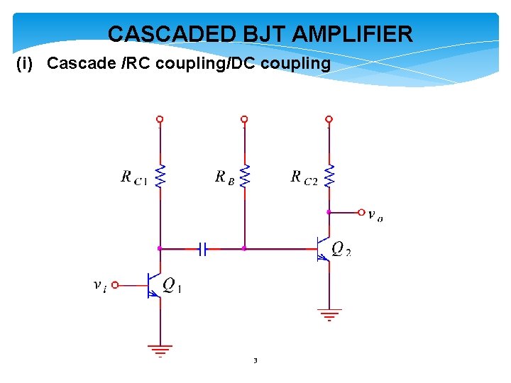
CASCADED BJT AMPLIFIER (i) Cascade /RC coupling/DC coupling 3

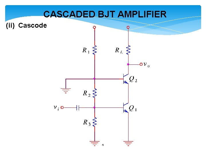
CASCADED BJT AMPLIFIER (ii) Cascode 4

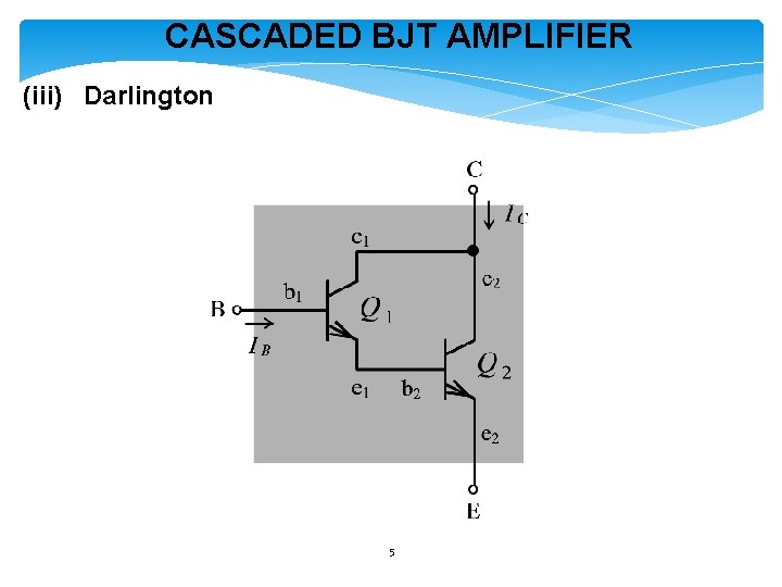
CASCADED BJT AMPLIFIER (iii) Darlington 5

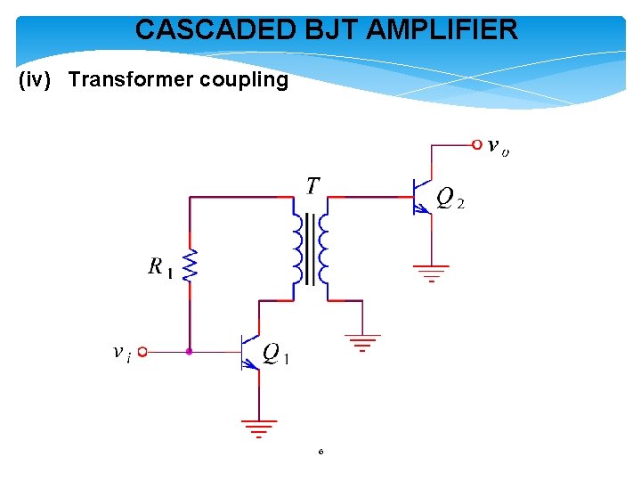
CASCADED BJT AMPLIFIER (iv) Transformer coupling 6

CASCADED BJT AMPLIFIER i) Cascade connection RC coupling - Coupling capacitor couples the signal from one stage to the another stage and block dc voltage from one stage to the another stage. - The signal developed across the collector resistor of each stage is coupled into the base of the next stage - The overall gain = product of the individual gain 7

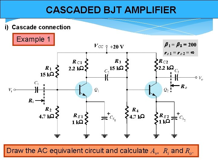
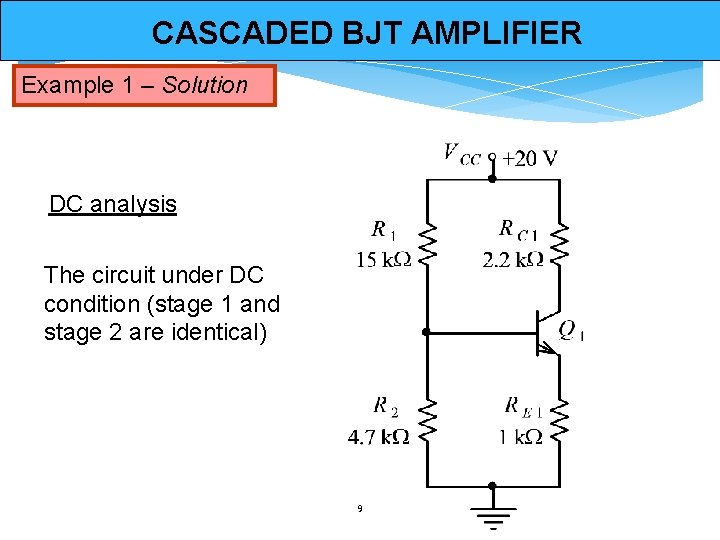
CASCADED BJT AMPLIFIER i) Cascade connection Example 1 R 1 15 k. W V CC RC 1 2. 2 k. W b 1 = b 2 = 200 +20 V ro 1 = ro 2 = ¥ R 3 15 k. W RC 2 2. 2 k. W Ro Ri R 2 4. 7 k. W RE 1 1 k. W R 4 4. 7 k. W RE 2 1 k. W Draw the AC equivalent circuit and calculate Av, Ri and Ro. 8

CASCADED BJT AMPLIFIER Example 1 – Solution DC analysis The circuit under DC condition (stage 1 and stage 2 are identical) 9

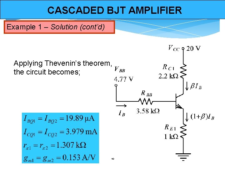
CASCADED BJT AMPLIFIER Example 1 – Solution (cont’d) Applying Thevenin’s theorem, the circuit becomes; 10

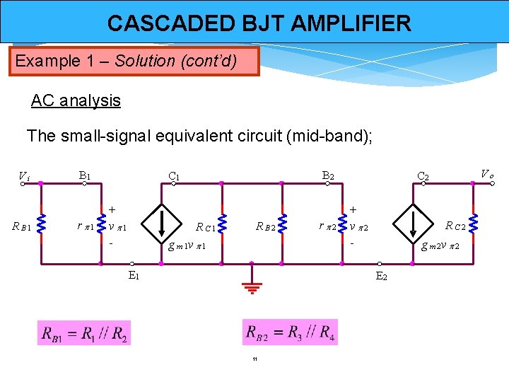
CASCADED BJT AMPLIFIER Example 1 – Solution (cont’d) AC analysis The small-signal equivalent circuit (mid-band); Vi R B 1 r 1 B 2 C 1 + v 1 - RC 1 R B 2 g m 1 v 1 E 1 r 2 + v 2 - RC 2 g m 2 v 2 E 2 11 Vo C 2

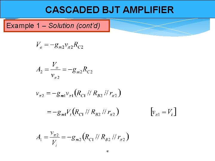
CASCADED BJT AMPLIFIER Example 1 – Solution (cont’d) 12

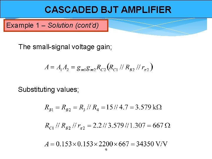
CASCADED BJT AMPLIFIER Example 1 – Solution (cont’d) The small-signal voltage gain; Substituting values; 13

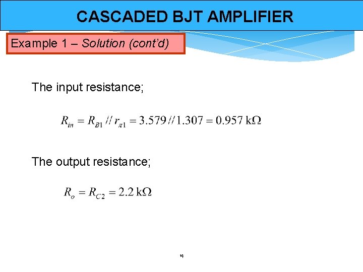
CASCADED BJT AMPLIFIER Example 1 – Solution (cont’d) The input resistance; The output resistance; 14

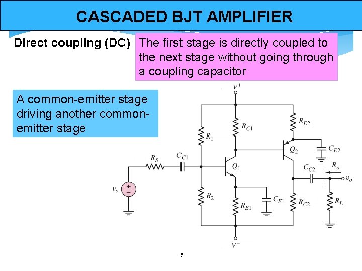
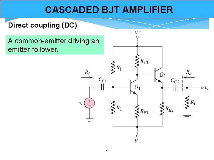
CASCADED BJT AMPLIFIER Direct coupling (DC) The first stage is directly coupled to the next stage without going through a coupling capacitor A common-emitter stage driving another commonemitter stage 15

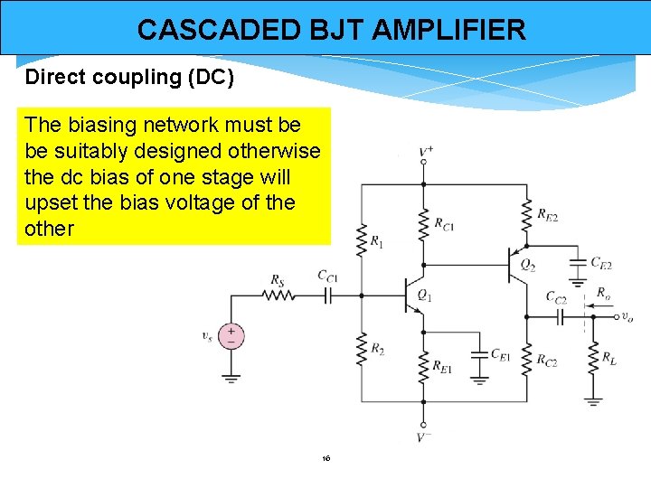
CASCADED BJT AMPLIFIER Direct coupling (DC) The biasing network must be be suitably designed otherwise the dc bias of one stage will upset the bias voltage of the other 16

CASCADED BJT AMPLIFIER Direct coupling (DC) A common-emitter driving an emitter-follower. 17

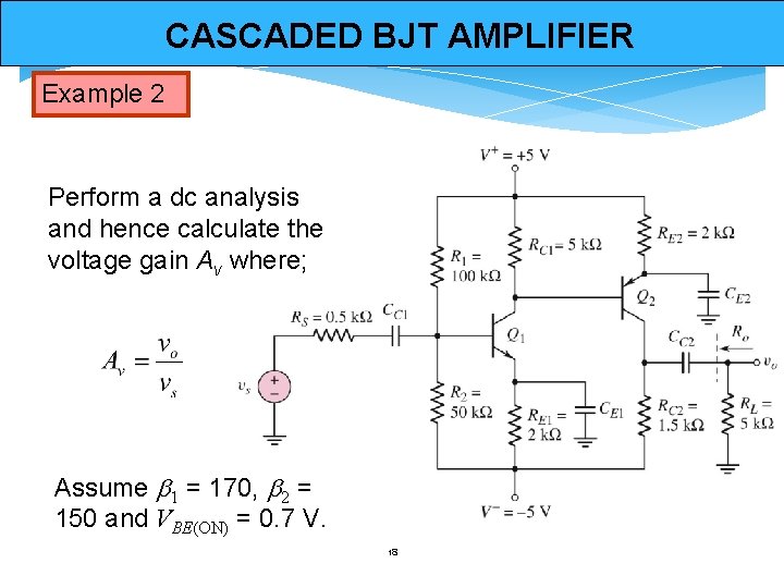
CASCADED BJT AMPLIFIER Example 2 Perform a dc analysis and hence calculate the voltage gain Av where; Assume 1 = 170, 2 = 150 and VBE(ON) = 0. 7 V. 18

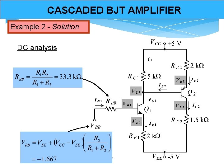
CASCADED BJT AMPLIFIER Example 2 - Solution DC analysis 19

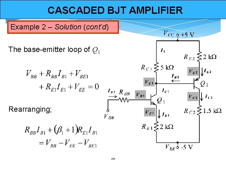
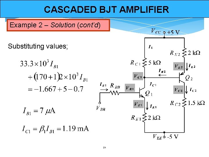
CASCADED BJT AMPLIFIER Example 2 – Solution (cont’d) The base-emitter loop of Q 1 Rearranging; 20

CASCADED BJT AMPLIFIER Example 2 – Solution (cont’d) Substituting values; 21

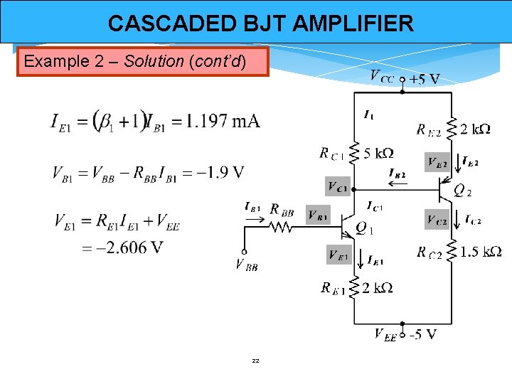
CASCADED BJT AMPLIFIER Example 2 – Solution (cont’d) 22

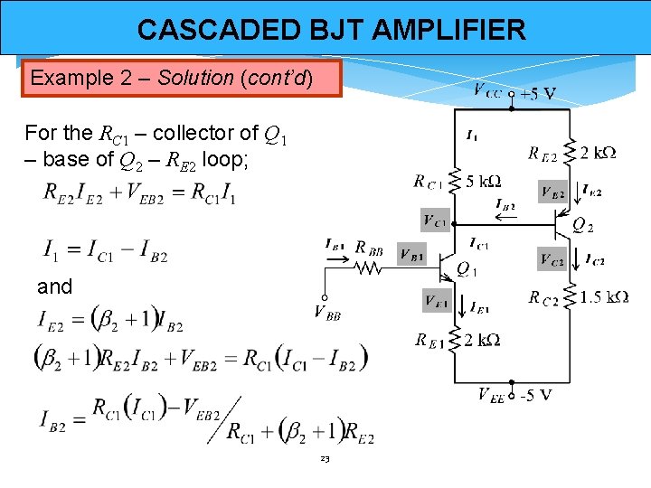
CASCADED BJT AMPLIFIER Example 2 – Solution (cont’d) For the RC 1 – collector of Q 1 – base of Q 2 – RE 2 loop; and 23

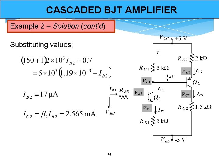
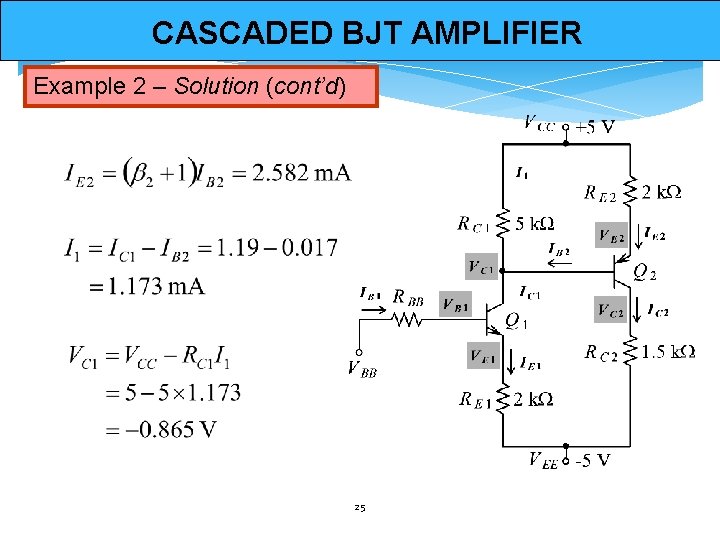
CASCADED BJT AMPLIFIER Example 2 – Solution (cont’d) Substituting values; 24

CASCADED BJT AMPLIFIER Example 2 – Solution (cont’d) 25

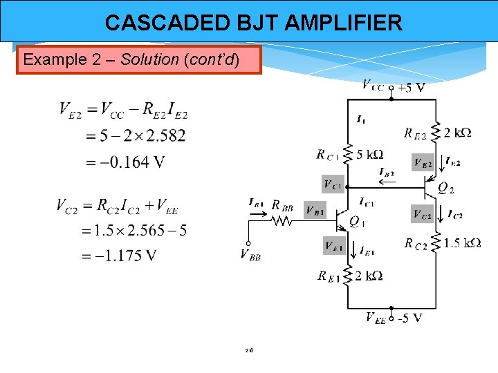
CASCADED BJT AMPLIFIER Example 2 – Solution (cont’d) 26

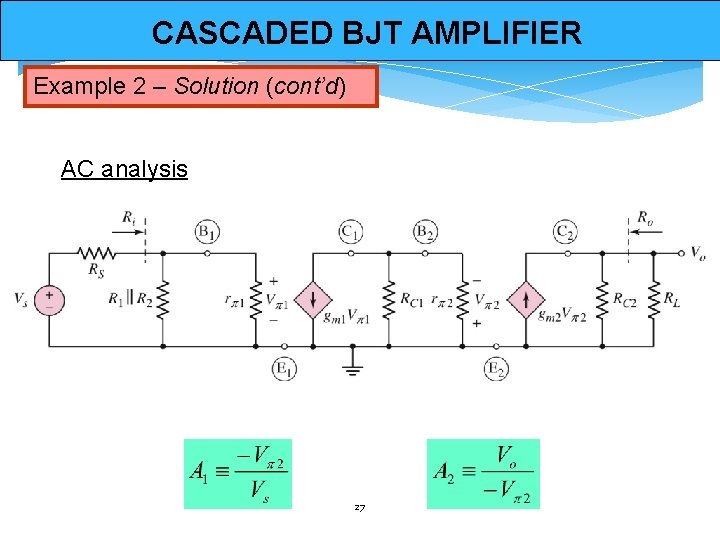
CASCADED BJT AMPLIFIER Example 2 – Solution (cont’d) AC analysis 27

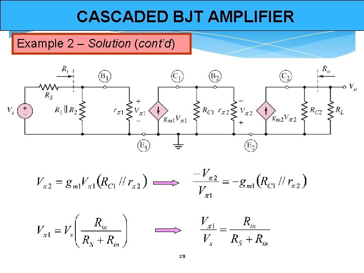
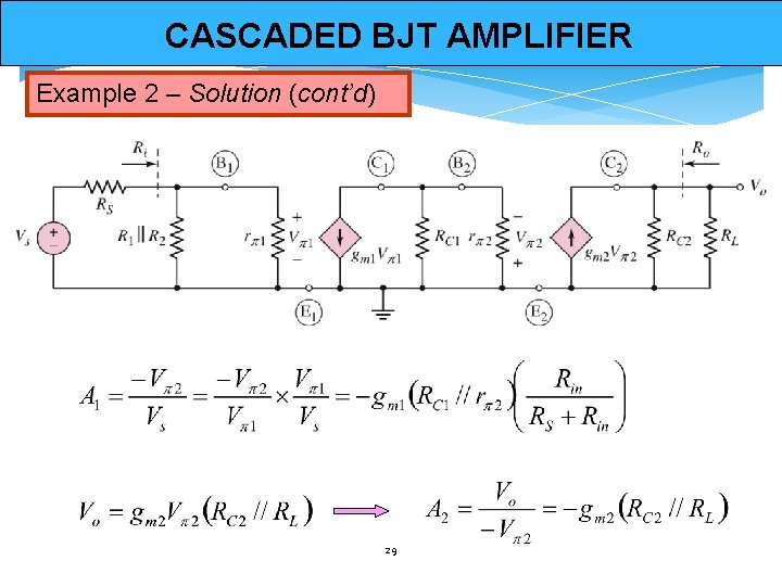
CASCADED BJT AMPLIFIER Example 2 – Solution (cont’d) 28

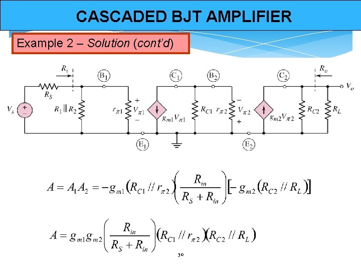
CASCADED BJT AMPLIFIER Example 2 – Solution (cont’d) 29

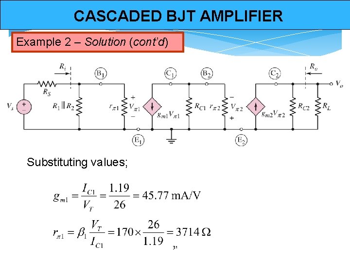
CASCADED BJT AMPLIFIER Example 2 – Solution (cont’d) 30

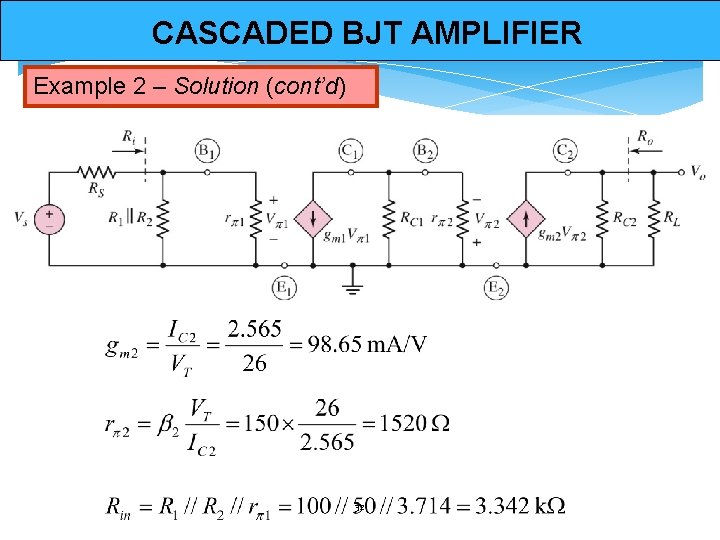
CASCADED BJT AMPLIFIER Example 2 – Solution (cont’d) Substituting values; 31

CASCADED BJT AMPLIFIER Example 2 – Solution (cont’d) 32

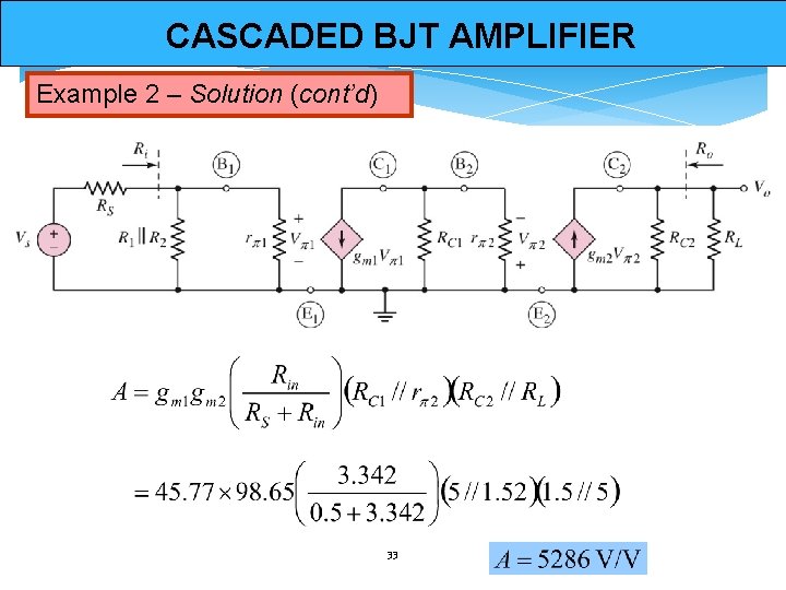
CASCADED BJT AMPLIFIER Example 2 – Solution (cont’d) 33

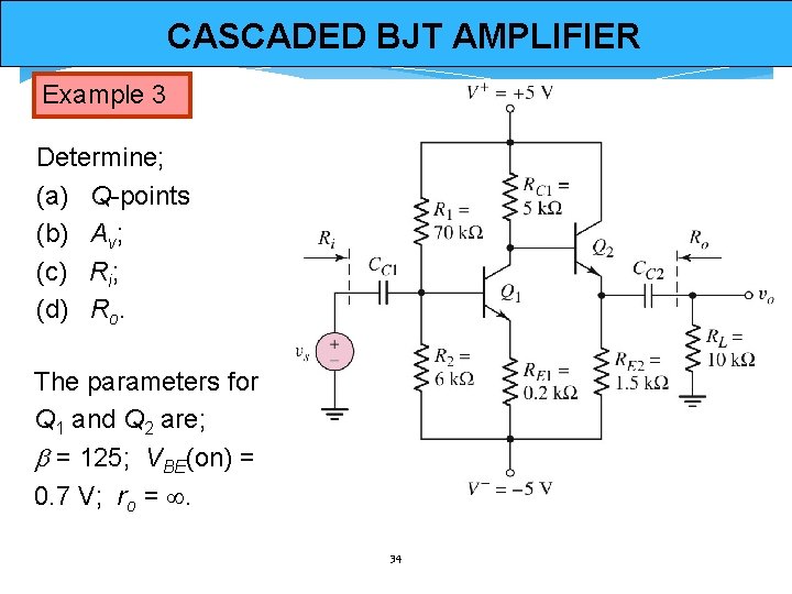
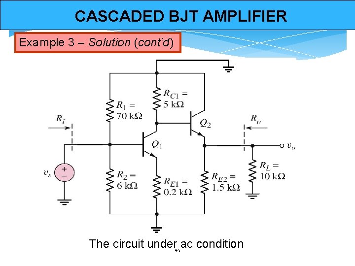
CASCADED BJT AMPLIFIER Example 3 Determine; (a) Q-points (b) Av; (c) Ri; (d) Ro. The parameters for Q 1 and Q 2 are; = 125; VBE(on) = 0. 7 V; ro = . 34

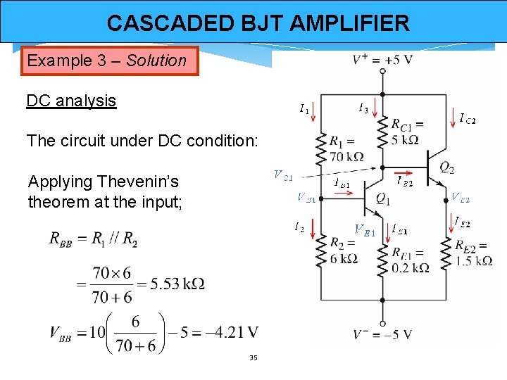
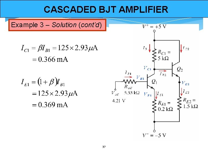
CASCADED BJT AMPLIFIER Example 3 – Solution DC analysis The circuit under DC condition: Applying Thevenin’s theorem at the input; 35

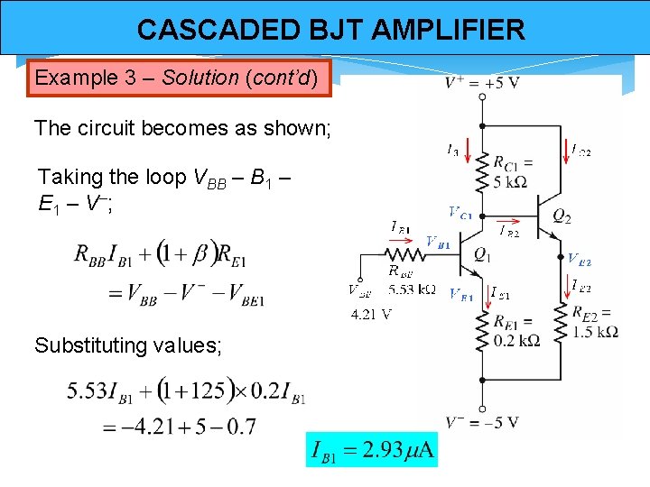
CASCADED BJT AMPLIFIER Example 3 – Solution (cont’d) The circuit becomes as shown; Taking the loop VBB – B 1 – E 1 – V –; Substituting values; 36

CASCADED BJT AMPLIFIER Example 3 – Solution (cont’d) 37

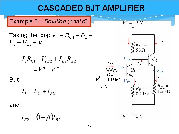
CASCADED BJT AMPLIFIER Example 3 – Solution (cont’d) Taking the loop V+ – RC 1 – B 2 – E 2 – RE 2 – V–; But; and; 38

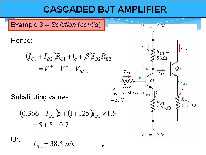
CASCADED BJT AMPLIFIER Example 3 – Solution (cont’d) Hence; Substituting values; Or; 39

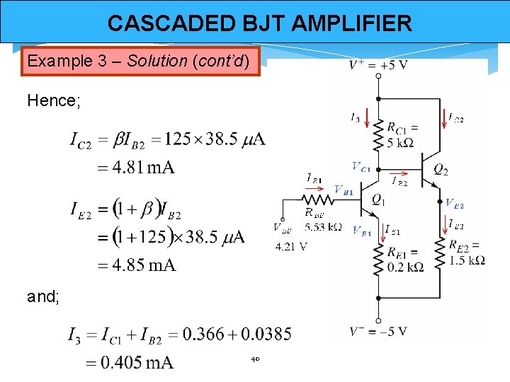
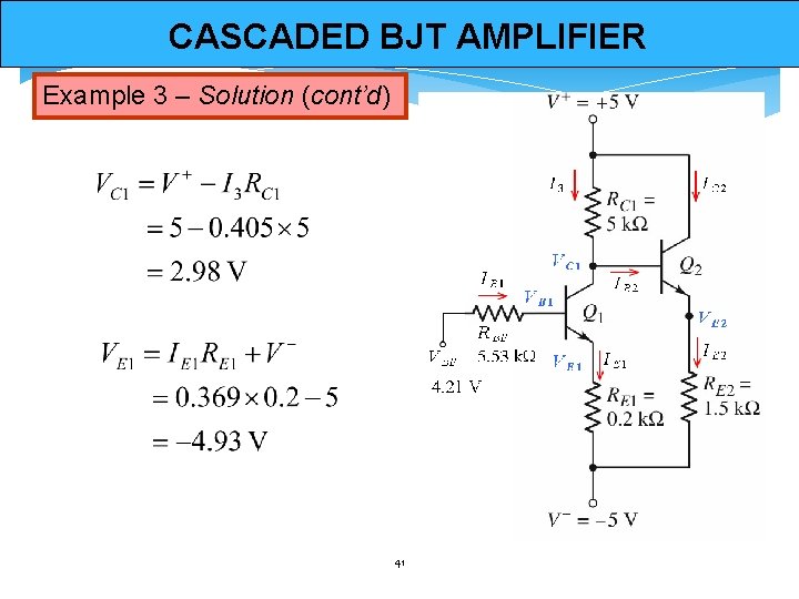
CASCADED BJT AMPLIFIER Example 3 – Solution (cont’d) Hence; and; 40

CASCADED BJT AMPLIFIER Example 3 – Solution (cont’d) 41

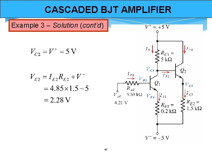
CASCADED BJT AMPLIFIER Example 3 – Solution (cont’d) 42

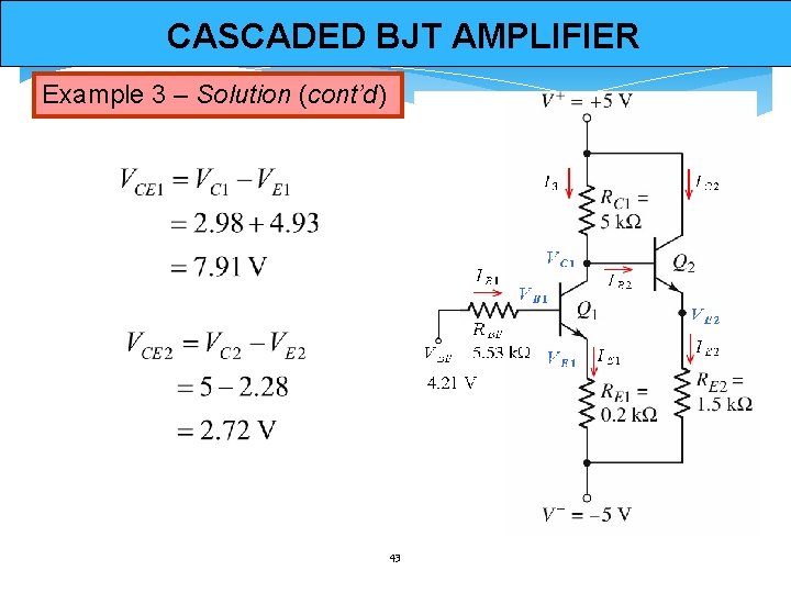
CASCADED BJT AMPLIFIER Example 3 – Solution (cont’d) 43

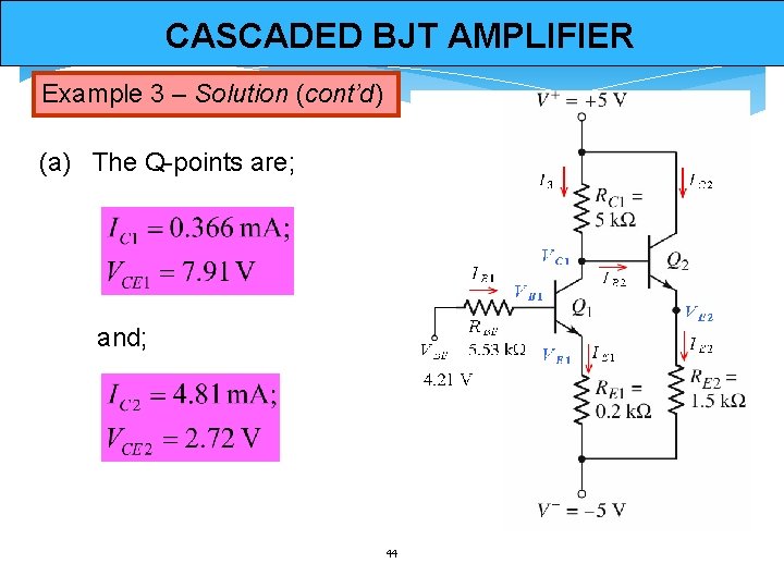
CASCADED BJT AMPLIFIER Example 3 – Solution (cont’d) (a) The Q-points are; and; 44

CASCADED BJT AMPLIFIER Example 3 – Solution (cont’d) The circuit under 45 ac condition

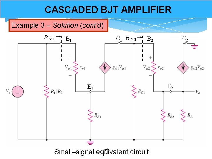
CASCADED BJT AMPLIFIER Example 3 – Solution (cont’d) 46 Small–signal equivalent circuit

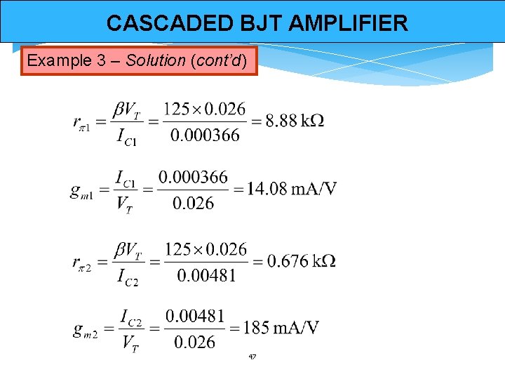
CASCADED BJT AMPLIFIER Example 3 – Solution (cont’d) 47

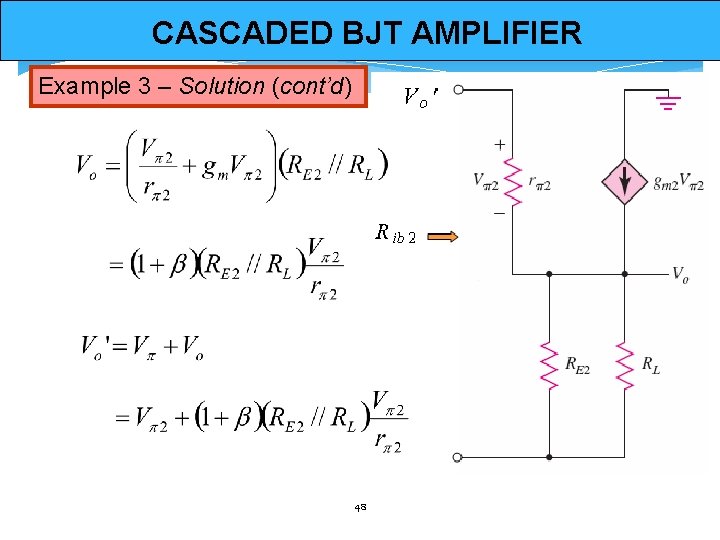
CASCADED BJT AMPLIFIER Example 3 – Solution (cont’d) 48

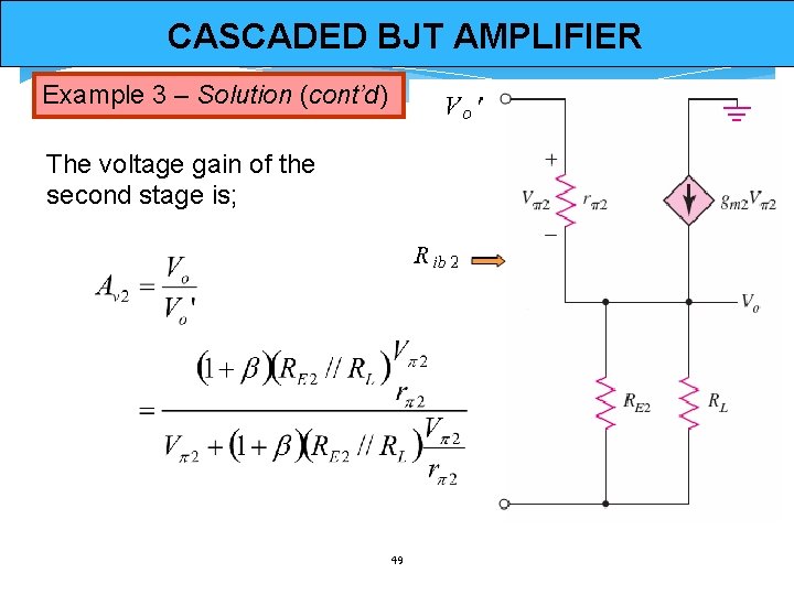
CASCADED BJT AMPLIFIER Example 3 – Solution (cont’d) The voltage gain of the second stage is; 49

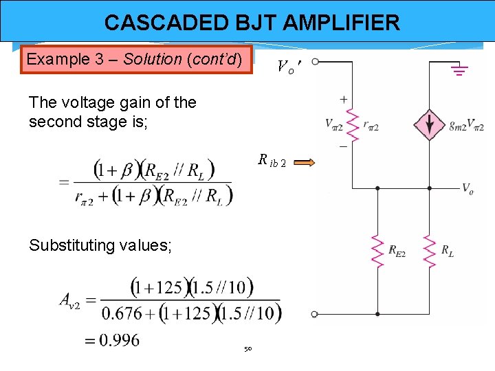
CASCADED BJT AMPLIFIER Example 3 – Solution (cont’d) The voltage gain of the second stage is; Substituting values; 50

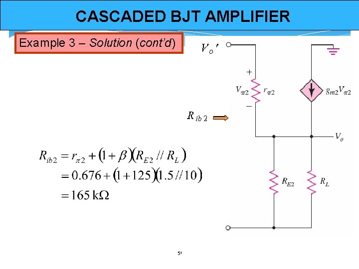
CASCADED BJT AMPLIFIER Example 3 – Solution (cont’d) 51

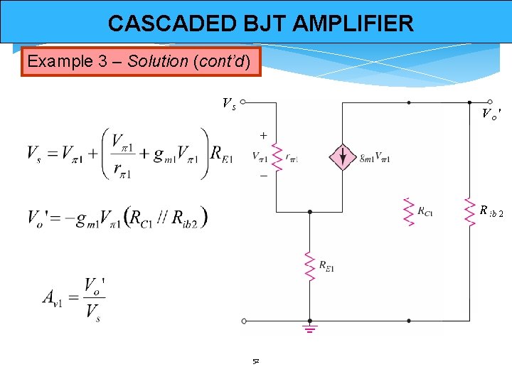
CASCADED BJT AMPLIFIER Example 3 – Solution (cont’d) 52

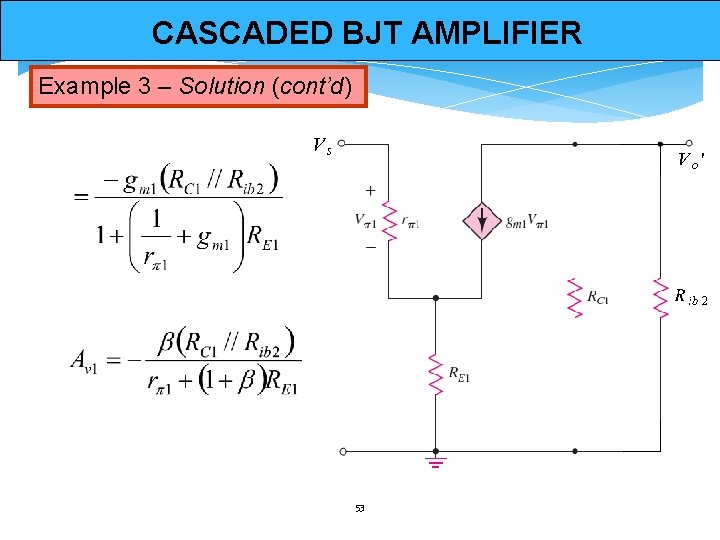
CASCADED BJT AMPLIFIER Example 3 – Solution (cont’d) 53

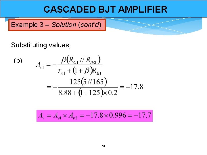
CASCADED BJT AMPLIFIER Example 3 – Solution (cont’d) Substituting values; (b) 54

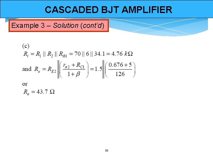
CASCADED BJT AMPLIFIER Example 3 – Solution (cont’d) 55

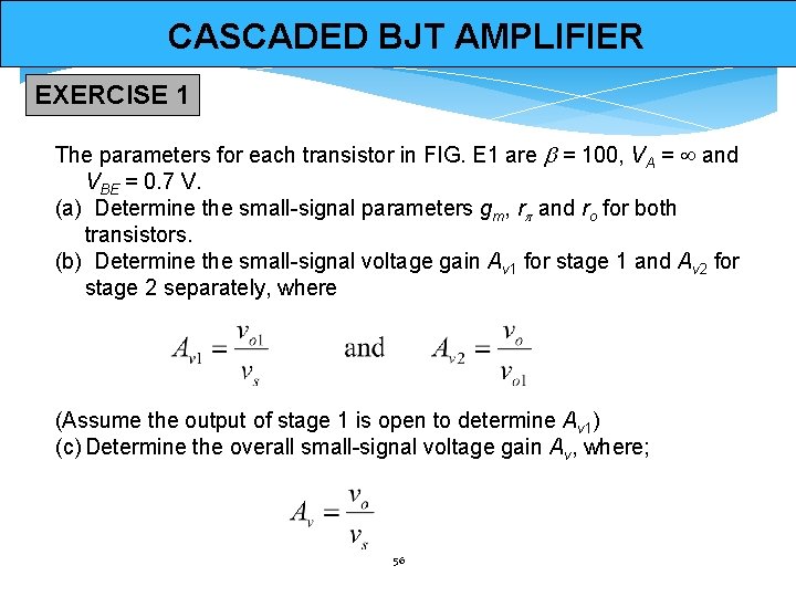
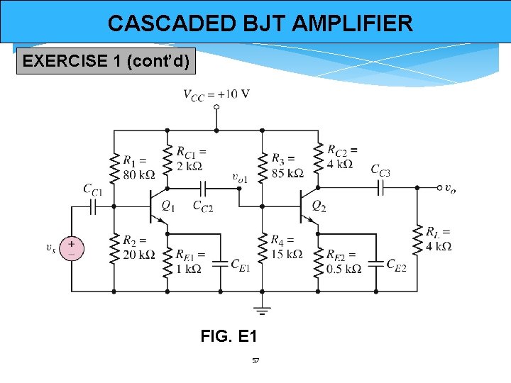
CASCADED BJT AMPLIFIER EXERCISE 1 The parameters for each transistor in FIG. E 1 are = 100, VA = and VBE = 0. 7 V. (a) Determine the small-signal parameters gm, r and ro for both transistors. (b) Determine the small-signal voltage gain Av 1 for stage 1 and Av 2 for stage 2 separately, where (Assume the output of stage 1 is open to determine Av 1) (c) Determine the overall small-signal voltage gain Av, where; 56

CASCADED BJT AMPLIFIER EXERCISE 1 (cont’d) FIG. E 1 57