DMA and CRT Controllers 1 8257 DMA CONTROLLER
- Slides: 54

DMA and CRT Controllers 1

8257: DMA CONTROLLER • The Direct Memory Access or DMA mode of data transfer is the fastest amongst all the modes of data transfer. • In this mode, the device may transfer data directly to / from memory without any interference from the CPU. • The device requests the CPU (through a DMA controller) to hold its data, address and control bus, so that the device may transfer data directly to/from memory. • The DMA data transfer is initiated only after receiving HLDA signal from the CPU. • For facilitating DMA type of data transfer between several devices, a DMA controller may be used. 2

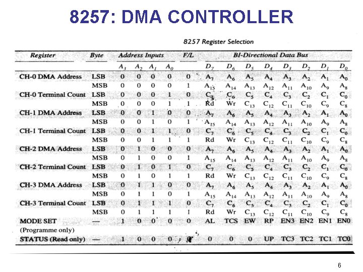
8257: DMA CONTROLLER • Intel’s 8251 is a four channel DMA controller designed to be interfaced with their family of microprocessors. • The 8257 performs the DMA operation over four independent DMA channels. • Each of the four channels of 8257 has a pair of two 16 bit registers, viz. DMA address register and terminal count register. • Also, there are two common registers for all the channels, namely, mode set register. • Thus there a total of ten registers. The CPU selects one of these ten registers using address lines A 0 – A 3. 3

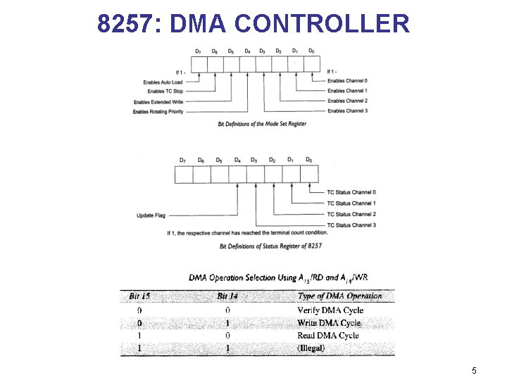
8257: DMA CONTROLLER • DMA address register – Each DMA channel has one DMA address register. – The function of this register is to store the address of the starting memory location, which will be accessed by the DMA channel. • Terminal Count Register – Each of the four DMA channels of 8257 has one terminal count register (TC)> this 16 bit register is used for ascertaining that the data transfer through a DMA channel ceases or stops after the required number of cycles. • Mode Set Register – The Mode Set Register is used for programming the 8257 as per the requirement of system. 4

8257: DMA CONTROLLER 5

8257: DMA CONTROLLER 6

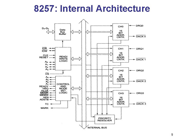
8257: DMA CONTROLLER • Status register – The lower order 4 bits of register contain the terminal count status for the four individual channels. – If any of these bits is set, it indicates that the specific channel has reached the terminal count condition. • The 8 bit, tristate, bidirectional buffer interfaces the internal bus of 8257 with the external system under the control of various control signals. 7

8257: DMA CONTROLLER • In the slave mode, the read/write logic accepts the I/O Read or I/O write signals, decodes the A 0 – A 3 lines and either writes the contents of the data bus to the addressed internal register or reads the contents of the selected register depending upon whether IOW or IOR signal is activated. • In master mode, the read/ write logic generates IOR bar and IOW bar signals to control the data flow to or from the selected peripheral. • The control logic controls the sequences of operations and generates the required control signals like AEN, ADSTB, MEMR bar, MEMW, TC and MARK along with the address lines A 4 – A 7 in master mode. • The priority resolver resolves the priority of the four DMA channels depending upon whether normal priority or rotating priority is programmed. 8

8257: Internal Architecture 9

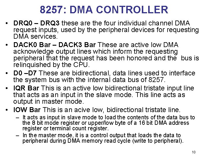
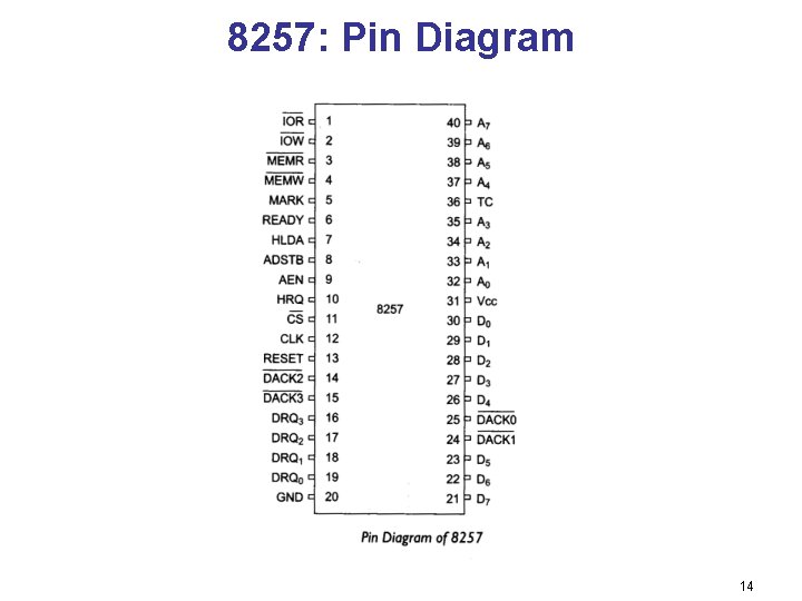
8257: DMA CONTROLLER • DRQ 0 – DRQ 3 these are the four individual channel DMA request inputs, used by the peripheral devices for requesting DMA services. • DACK 0 Bar – DACK 3 Bar These are active low DMA acknowledge output lines which inform the requesting peripheral that the request has been honored and the bus is relinquished by the CPU. • D 0 –D 7 These are bidirectional, data lines used to interface the system bus with the internal data bus of 8257. • IQR Bar This is an active low bidirectional tristate input line that acts as an input in the slave mode. This line acts as output in master mode. • IOW Bar This is an acive low, bidirectional tristate line. – It acts as input in slave mode to load the contents of the data bus to the 8 bit mode register or upper/low byte of a 16 bit DMA address register or terminal count register. – In the master mode, it is a control output that loads the data to peripheral during DMA memory read cycle (write to peripheral). 10

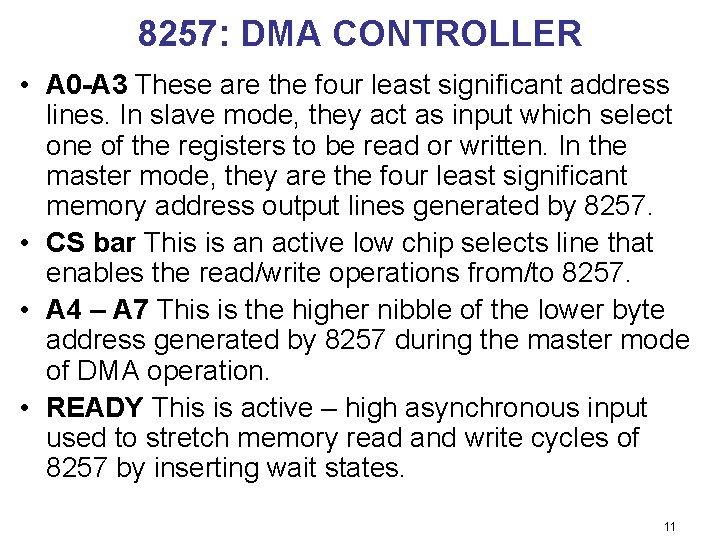
8257: DMA CONTROLLER • A 0 -A 3 These are the four least significant address lines. In slave mode, they act as input which select one of the registers to be read or written. In the master mode, they are the four least significant memory address output lines generated by 8257. • CS bar This is an active low chip selects line that enables the read/write operations from/to 8257. • A 4 – A 7 This is the higher nibble of the lower byte address generated by 8257 during the master mode of DMA operation. • READY This is active – high asynchronous input used to stretch memory read and write cycles of 8257 by inserting wait states. 11

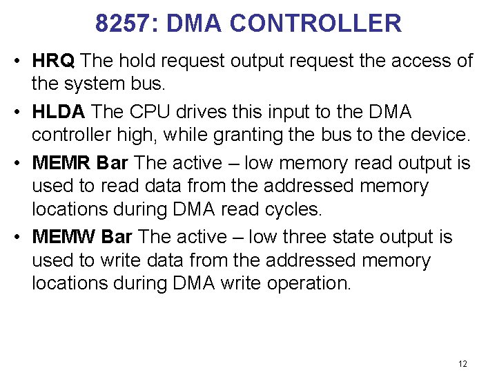
8257: DMA CONTROLLER • HRQ The hold request output request the access of the system bus. • HLDA The CPU drives this input to the DMA controller high, while granting the bus to the device. • MEMR Bar The active – low memory read output is used to read data from the addressed memory locations during DMA read cycles. • MEMW Bar The active – low three state output is used to write data from the addressed memory locations during DMA write operation. 12

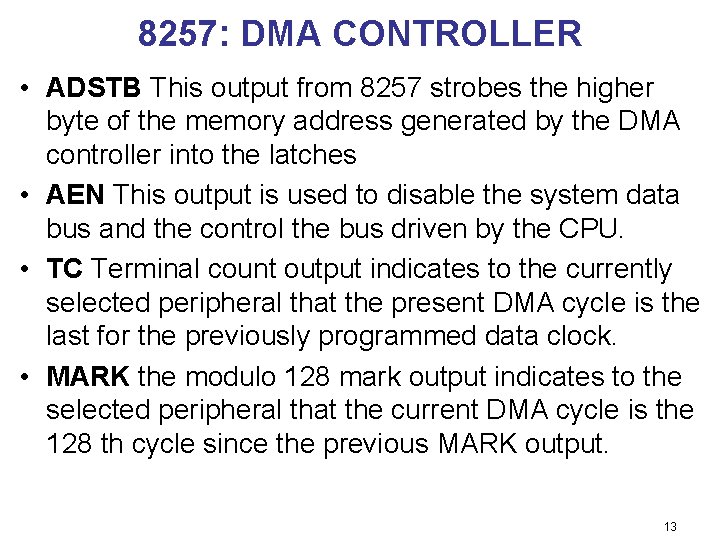
8257: DMA CONTROLLER • ADSTB This output from 8257 strobes the higher byte of the memory address generated by the DMA controller into the latches • AEN This output is used to disable the system data bus and the control the bus driven by the CPU. • TC Terminal count output indicates to the currently selected peripheral that the present DMA cycle is the last for the previously programmed data clock. • MARK the modulo 128 mark output indicates to the selected peripheral that the current DMA cycle is the 128 th cycle since the previous MARK output. 13

8257: Pin Diagram 14

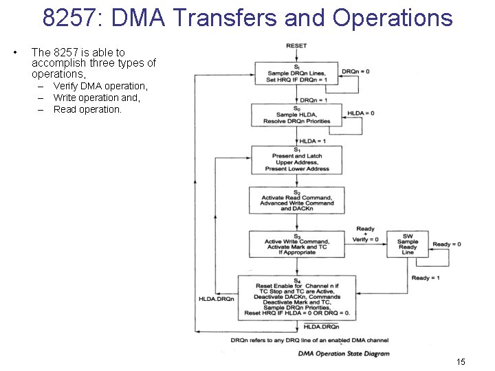
8257: DMA Transfers and Operations • The 8257 is able to accomplish three types of operations, – Verify DMA operation, – Write operation and, – Read operation. 15

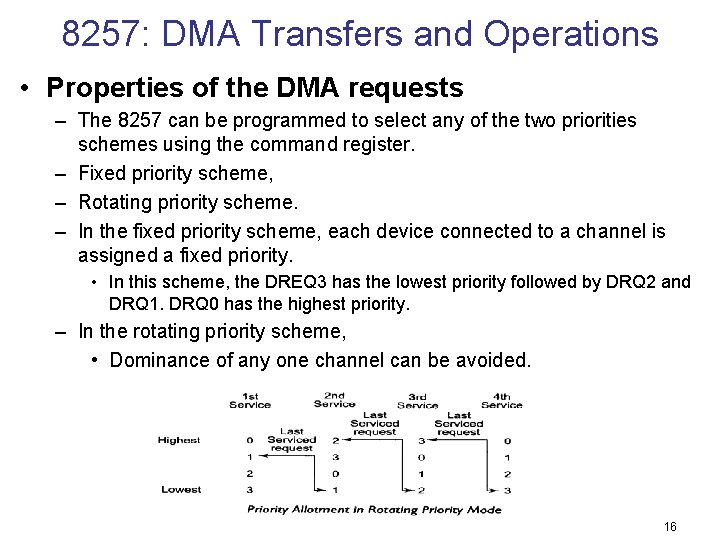
8257: DMA Transfers and Operations • Properties of the DMA requests – The 8257 can be programmed to select any of the two priorities schemes using the command register. – Fixed priority scheme, – Rotating priority scheme. – In the fixed priority scheme, each device connected to a channel is assigned a fixed priority. • In this scheme, the DREQ 3 has the lowest priority followed by DRQ 2 and DRQ 1. DRQ 0 has the highest priority. – In the rotating priority scheme, • Dominance of any one channel can be avoided. 16

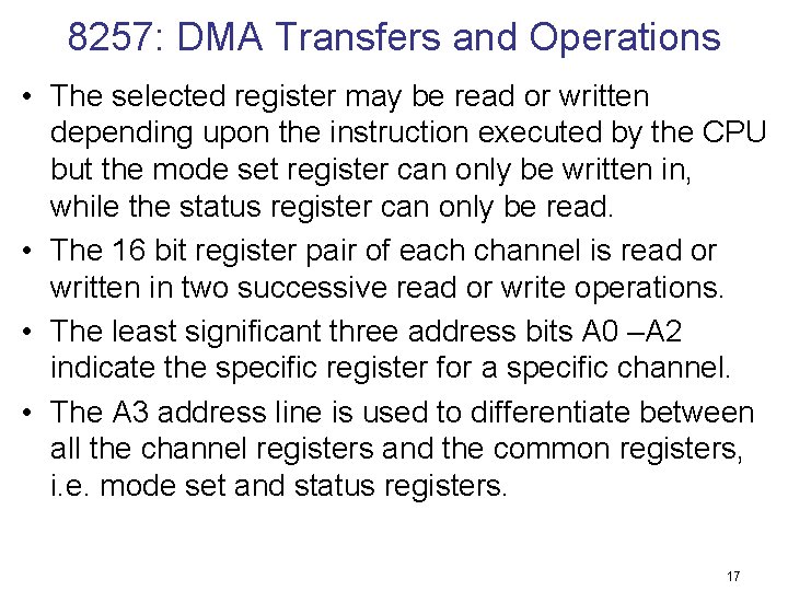
8257: DMA Transfers and Operations • The selected register may be read or written depending upon the instruction executed by the CPU but the mode set register can only be written in, while the status register can only be read. • The 16 bit register pair of each channel is read or written in two successive read or write operations. • The least significant three address bits A 0 –A 2 indicate the specific register for a specific channel. • The A 3 address line is used to differentiate between all the channel registers and the common registers, i. e. mode set and status registers. 17

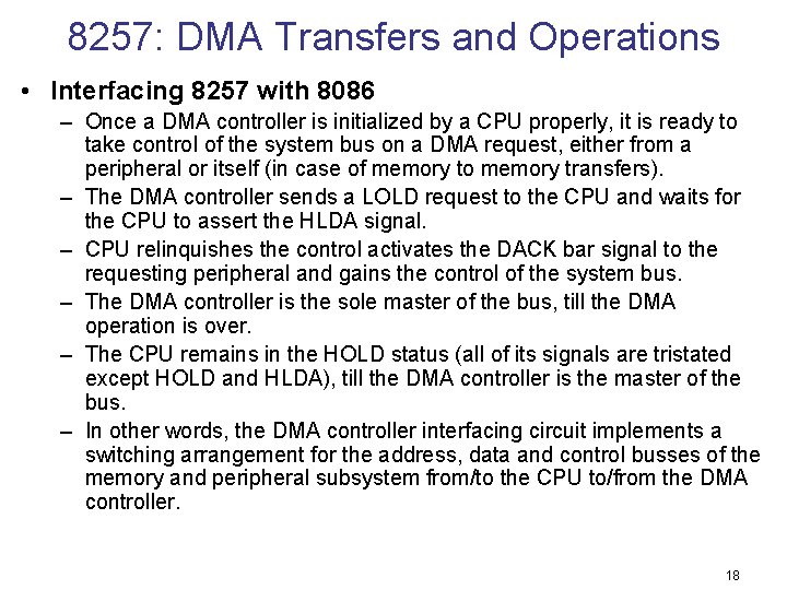
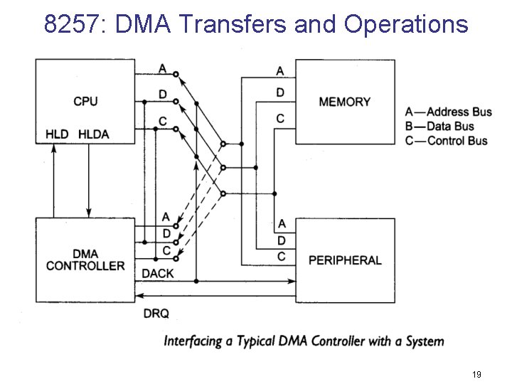
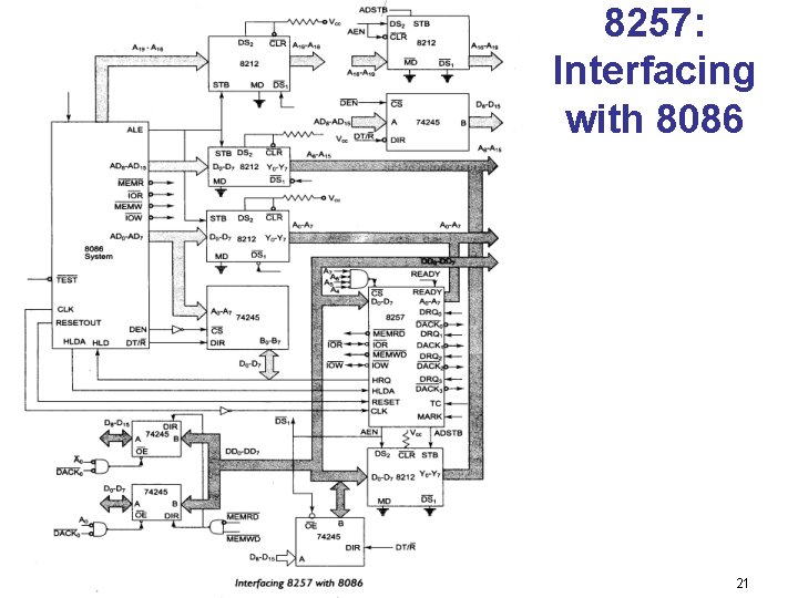
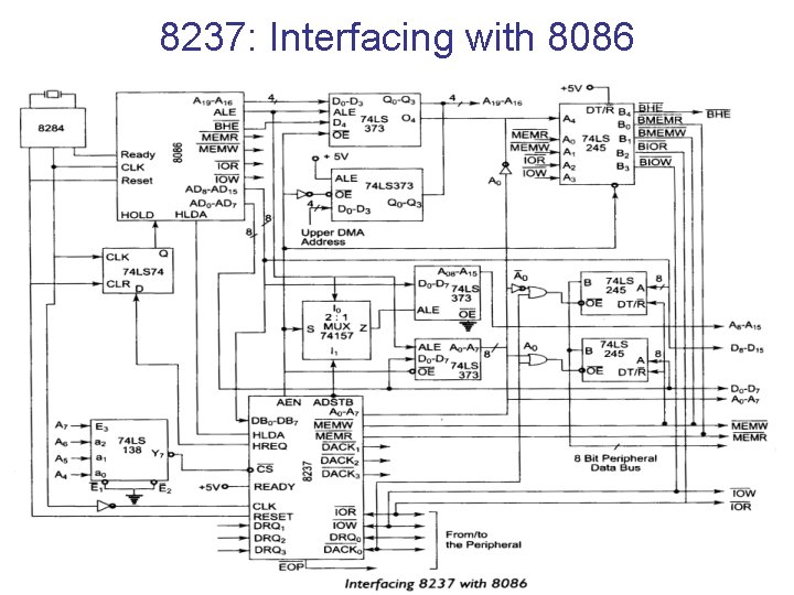
8257: DMA Transfers and Operations • Interfacing 8257 with 8086 – Once a DMA controller is initialized by a CPU properly, it is ready to take control of the system bus on a DMA request, either from a peripheral or itself (in case of memory to memory transfers). – The DMA controller sends a LOLD request to the CPU and waits for the CPU to assert the HLDA signal. – CPU relinquishes the control activates the DACK bar signal to the requesting peripheral and gains the control of the system bus. – The DMA controller is the sole master of the bus, till the DMA operation is over. – The CPU remains in the HOLD status (all of its signals are tristated except HOLD and HLDA), till the DMA controller is the master of the bus. – In other words, the DMA controller interfacing circuit implements a switching arrangement for the address, data and control busses of the memory and peripheral subsystem from/to the CPU to/from the DMA controller. 18

8257: DMA Transfers and Operations 19

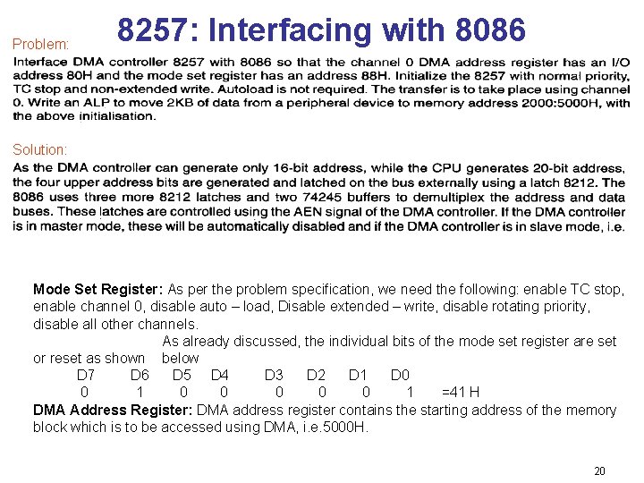
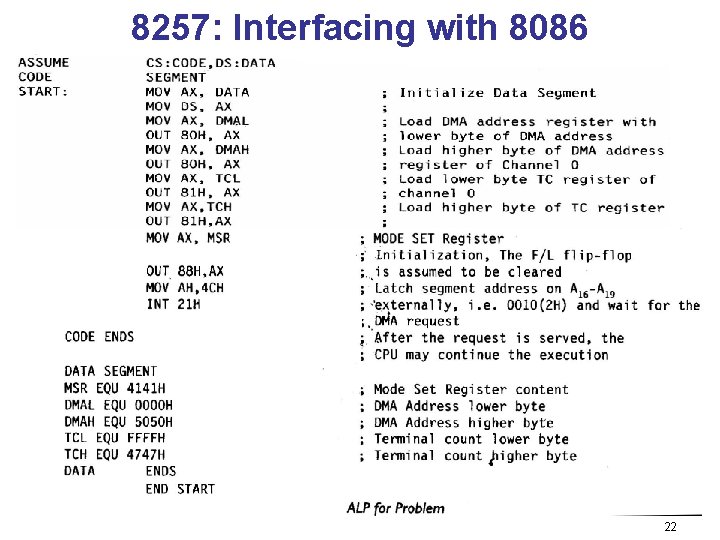
Problem: 8257: Interfacing with 8086 Solution: Mode Set Register: As per the problem specification, we need the following: enable TC stop, enable channel 0, disable auto – load, Disable extended – write, disable rotating priority, disable all other channels. As already discussed, the individual bits of the mode set register are set or reset as shown below D 7 D 6 D 5 D 4 D 3 D 2 D 1 D 0 0 1 0 0 0 1 =41 H DMA Address Register: DMA address register contains the starting address of the memory block which is to be accessed using DMA, i. e. 5000 H. 20

8257: Interfacing with 8086 21

8257: Interfacing with 8086 22

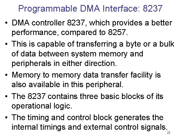
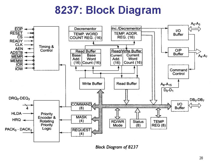
Programmable DMA Interface: 8237 • DMA controller 8237, which provides a better performance, compared to 8257. • This is capable of transferring a byte or a bulk of data between system memory and peripherals in either direction. • Memory to memory data transfer facility is also available in this peripheral. • The 8237 contains three basic blocks of its operational logic. • The timing and control block generates the internal timings and external control signals. 23

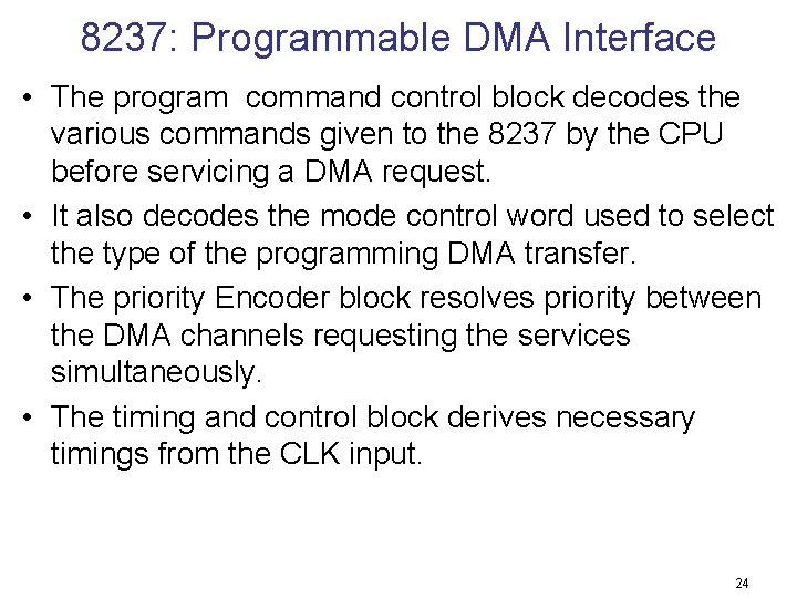
8237: Programmable DMA Interface • The program command control block decodes the various commands given to the 8237 by the CPU before servicing a DMA request. • It also decodes the mode control word used to select the type of the programming DMA transfer. • The priority Encoder block resolves priority between the DMA channels requesting the services simultaneously. • The timing and control block derives necessary timings from the CLK input. 24

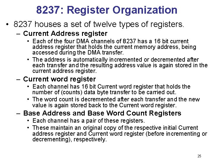
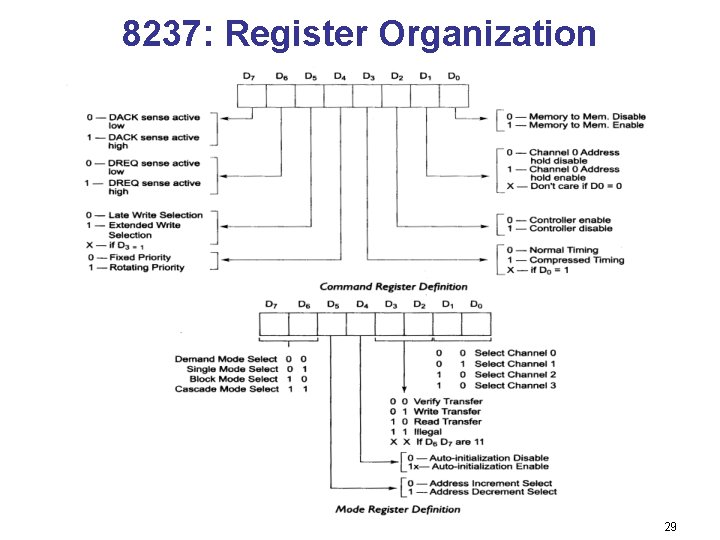
8237: Register Organization • 8237 houses a set of twelve types of registers. – Current Address register • Each of the four DMA channels of 8237 has a 16 bit current address register that holds the current memory address, being accessed during the DMA transfer. • The address is automatically incremented or decremented after each transfer and the resulting address value is again stored in the current address register. – Current word register • Each channel has 16 bit Current word register that holds the number of (counts) data byte transfer to be carried out. • The word count is decremented after each transfer and the new value is again stored back to the Current word register. – Base Address and Base Word Count Registers • Each channel has a pair of these registers. • These maintain an original copy of the respective initial Current address register and Current word register (before incrementing or decrementing), respectively. 25

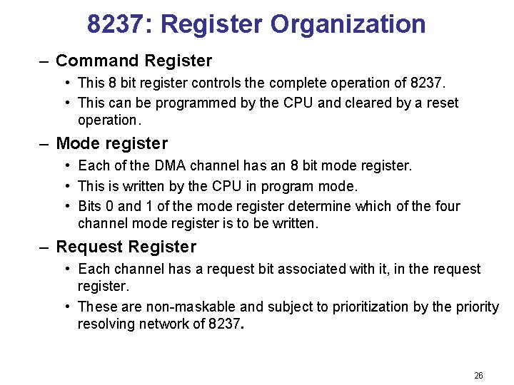
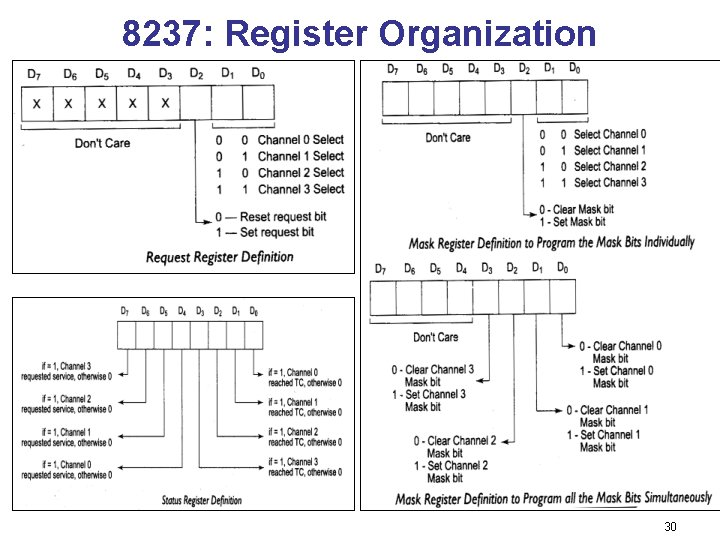
8237: Register Organization – Command Register • This 8 bit register controls the complete operation of 8237. • This can be programmed by the CPU and cleared by a reset operation. – Mode register • Each of the DMA channel has an 8 bit mode register. • This is written by the CPU in program mode. • Bits 0 and 1 of the mode register determine which of the four channel mode register is to be written. – Request Register • Each channel has a request bit associated with it, in the request register. • These are non-maskable and subject to prioritization by the priority resolving network of 8237. 26

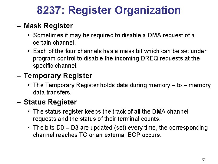
8237: Register Organization – Mask Register • Sometimes it may be required to disable a DMA request of a certain channel. • Each of the four channels has a mask bit which can be set under program control to disable the incoming DREQ requests at the specific channel. – Temporary Register • The Temporary Register holds data during memory – to – memory data transfers. – Status Register • The status register keeps the track of all the DMA channel requests and the status of their terminal counts. • The bits D 0 – D 3 are updated (set) every time, the corresponding channel reaches TC or an external EOP occurs. 27

8237: Block Diagram 28

8237: Register Organization 29

8237: Register Organization 30

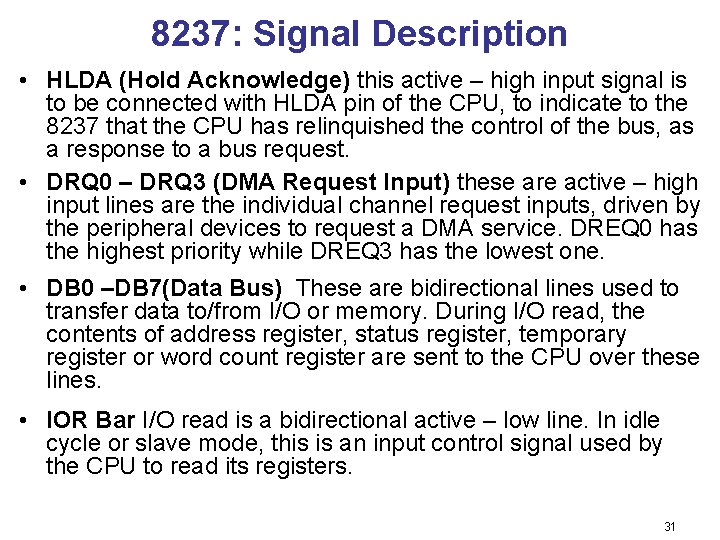
8237: Signal Description • HLDA (Hold Acknowledge) this active – high input signal is to be connected with HLDA pin of the CPU, to indicate to the 8237 that the CPU has relinquished the control of the bus, as a response to a bus request. • DRQ 0 – DRQ 3 (DMA Request Input) these are active – high input lines are the individual channel request inputs, driven by the peripheral devices to request a DMA service. DREQ 0 has the highest priority while DREQ 3 has the lowest one. • DB 0 –DB 7(Data Bus) These are bidirectional lines used to transfer data to/from I/O or memory. During I/O read, the contents of address register, status register, temporary register or word count register are sent to the CPU over these lines. • IOR Bar I/O read is a bidirectional active – low line. In idle cycle or slave mode, this is an input control signal used by the CPU to read its registers. 31

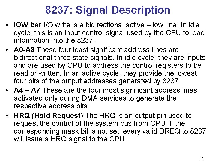
8237: Signal Description • IOW bar I/O write is a bidirectional active – low line. In idle cycle, this is an input control signal used by the CPU to load information into the 8237. • A 0 -A 3 These four least significant address lines are bidirectional three state signals. In idle cycle, they are inputs and are used by CPU to address the control registers to be read or written. In an active cycle, they provide the lowest four bits of the output addresses generated by 8237. • A 4 – A 7 These are the four most significant address lines activated only during DMA services to generate the respective address bits. • HRQ (Hold Request) The HRQ is an output pin used to request the control of the system bus from CPU. If the corresponding mask bit is not set, every valid DREQ to 8237 will issue a HRQ signal to the CPU. 32

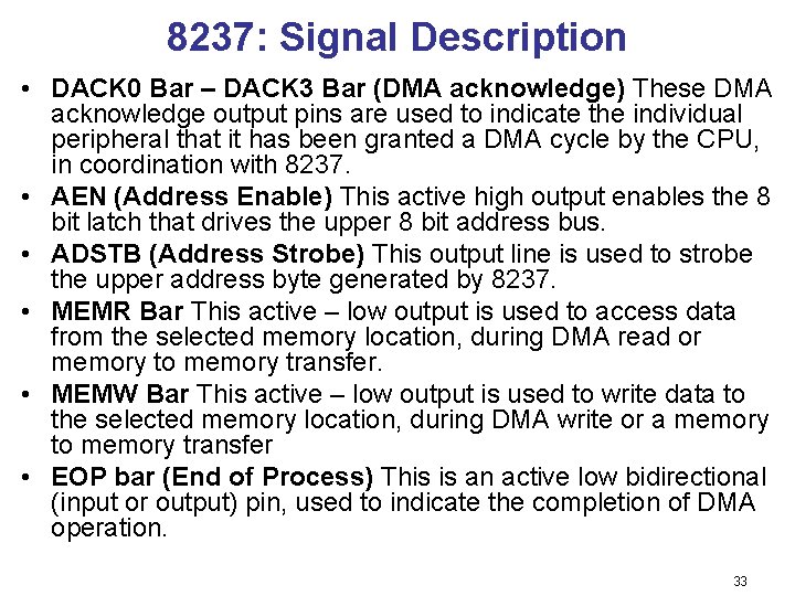
8237: Signal Description • DACK 0 Bar – DACK 3 Bar (DMA acknowledge) These DMA acknowledge output pins are used to indicate the individual peripheral that it has been granted a DMA cycle by the CPU, in coordination with 8237. • AEN (Address Enable) This active high output enables the 8 bit latch that drives the upper 8 bit address bus. • ADSTB (Address Strobe) This output line is used to strobe the upper address byte generated by 8237. • MEMR Bar This active – low output is used to access data from the selected memory location, during DMA read or memory to memory transfer. • MEMW Bar This active – low output is used to write data to the selected memory location, during DMA write or a memory to memory transfer • EOP bar (End of Process) This is an active low bidirectional (input or output) pin, used to indicate the completion of DMA operation. 33

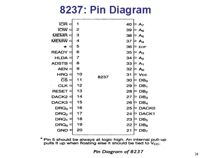
8237: Pin Diagram 34

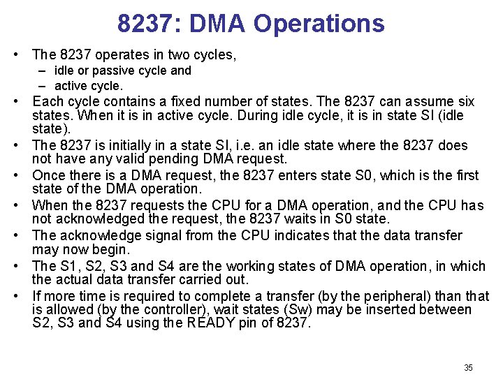
8237: DMA Operations • The 8237 operates in two cycles, – idle or passive cycle and – active cycle. • Each cycle contains a fixed number of states. The 8237 can assume six states. When it is in active cycle. During idle cycle, it is in state SI (idle state). • The 8237 is initially in a state SI, i. e. an idle state where the 8237 does not have any valid pending DMA request. • Once there is a DMA request, the 8237 enters state S 0, which is the first state of the DMA operation. • When the 8237 requests the CPU for a DMA operation, and the CPU has not acknowledged the request, the 8237 waits in S 0 state. • The acknowledge signal from the CPU indicates that the data transfer may now begin. • The S 1, S 2, S 3 and S 4 are the working states of DMA operation, in which the actual data transfer carried out. • If more time is required to complete a transfer (by the peripheral) than that is allowed (by the controller), wait states (Sw) may be inserted between S 2, S 3 and S 4 using the READY pin of 8237. 35

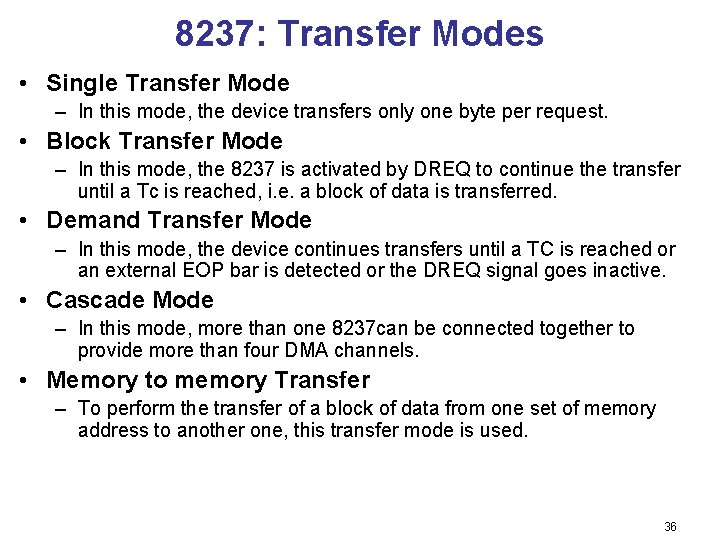
8237: Transfer Modes • Single Transfer Mode – In this mode, the device transfers only one byte per request. • Block Transfer Mode – In this mode, the 8237 is activated by DREQ to continue the transfer until a Tc is reached, i. e. a block of data is transferred. • Demand Transfer Mode – In this mode, the device continues transfers until a TC is reached or an external EOP bar is detected or the DREQ signal goes inactive. • Cascade Mode – In this mode, more than one 8237 can be connected together to provide more than four DMA channels. • Memory to memory Transfer – To perform the transfer of a block of data from one set of memory address to another one, this transfer mode is used. 36

8237: Address Generation • The 8237 multiplexes the eight higher order bits (A 8 – A 15) on data lines. • The state (idle) is used to transfer the higher order address bits to a latch from which they are to be placed on the address bus. • The falling edge of the Address Strobe (ADSTB) signal is used to load these higher address bits from data lines to the latch while that of AEN is used to place the same to the system address bus through a tristate buffer. • The lower order address A 0 – A 7 is directly generated by 8237 on its A 0 –A 7 pins. 37

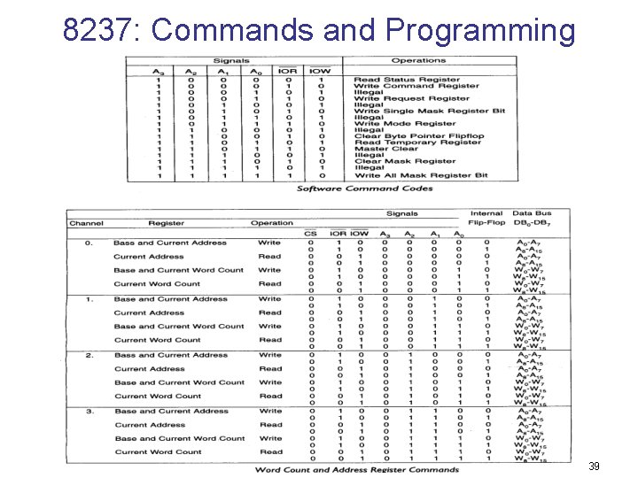
8237: Commands and Programming • There are several commands which can be executed by 8237 when it is in program condition. • Clear First/Last Flip-Flop – as we have discussed in case of 8257, there exists an internal flip-flop in 8237 also which is called First/Last Flip-flop (F/L ff). This flip flop output decides whether the lower byte or the upper byte of the selected 16 bit register will be read or written. • Clear Mask Register – as has been described earlier, a mask set register when set, may disable the DMA channels, so that the DMA requests are not entertained. • Master Clear Command – Using this command, all the internal registers of 8237 are cleared, while all the bits of the mask registers are set. This means after executing this command, the DMA controller disables all the DMA channels and enters an idle cycle. 38

8237: Commands and Programming 39

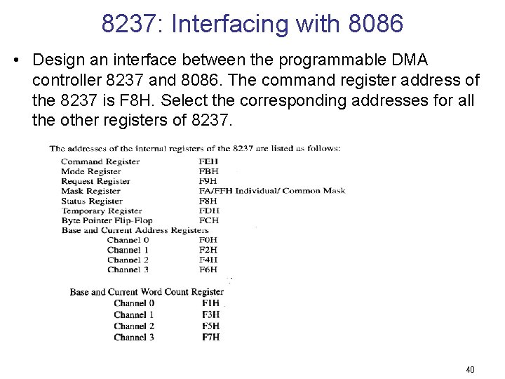
8237: Interfacing with 8086 • Design an interface between the programmable DMA controller 8237 and 8086. The command register address of the 8237 is F 8 H. Select the corresponding addresses for all the other registers of 8237. 40

8237: Interfacing with 8086 41

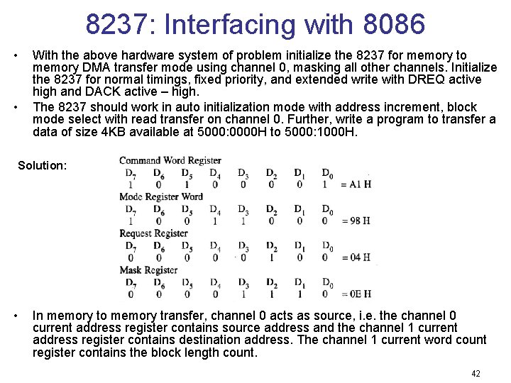
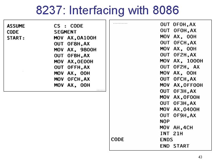
8237: Interfacing with 8086 • • With the above hardware system of problem initialize the 8237 for memory to memory DMA transfer mode using channel 0, masking all other channels. Initialize the 8237 for normal timings, fixed priority, and extended write with DREQ active high and DACK active – high. The 8237 should work in auto initialization mode with address increment, block mode select with read transfer on channel 0. Further, write a program to transfer a data of size 4 KB available at 5000: 0000 H to 5000: 1000 H. Solution: • In memory to memory transfer, channel 0 acts as source, i. e. the channel 0 current address register contains source address and the channel 1 current address register contains destination address. The channel 1 current word count register contains the block length count. 42

8237: Interfacing with 8086 43

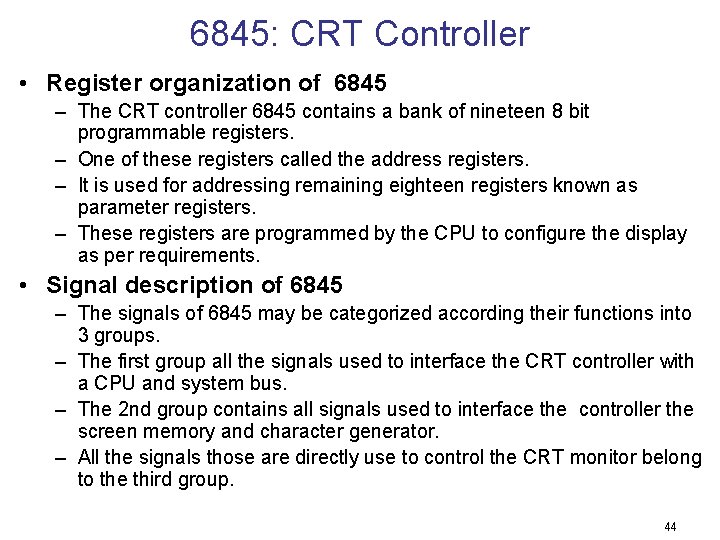
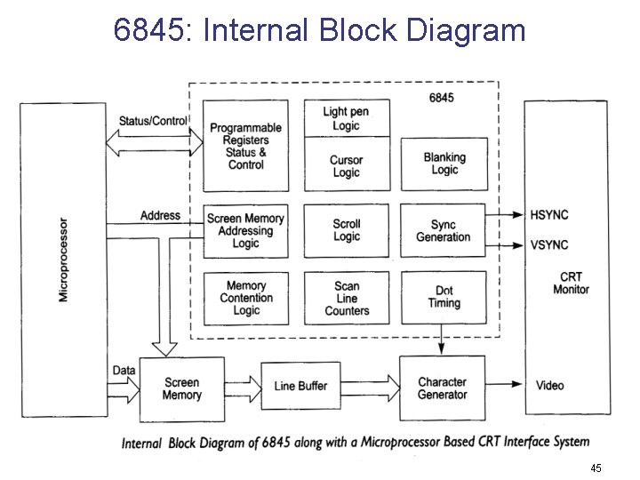
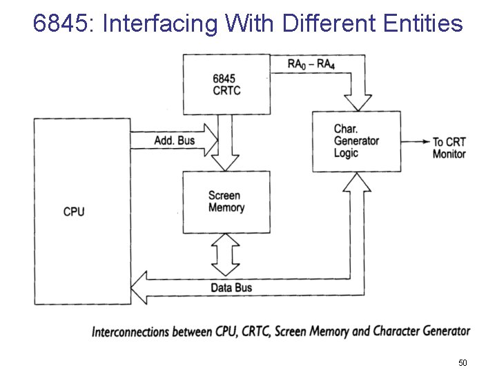
6845: CRT Controller • Register organization of 6845 – The CRT controller 6845 contains a bank of nineteen 8 bit programmable registers. – One of these registers called the address registers. – It is used for addressing remaining eighteen registers known as parameter registers. – These registers are programmed by the CPU to configure the display as per requirements. • Signal description of 6845 – The signals of 6845 may be categorized according their functions into 3 groups. – The first group all the signals used to interface the CRT controller with a CPU and system bus. – The 2 nd group contains all signals used to interface the controller the screen memory and character generator. – All the signals those are directly use to control the CRT monitor belong to the third group. 44

6845: Internal Block Diagram 45

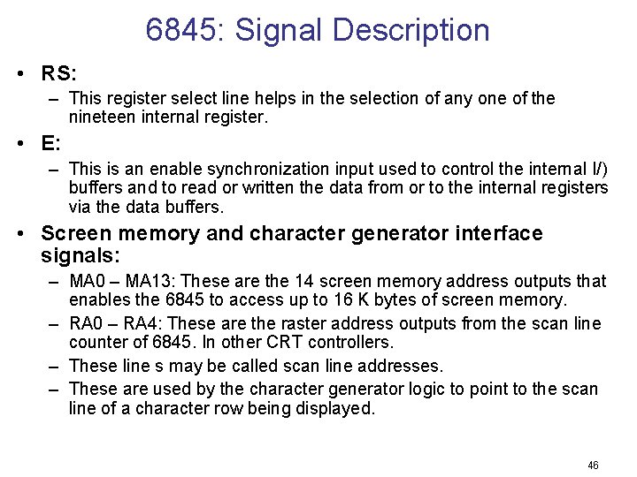
6845: Signal Description • RS: – This register select line helps in the selection of any one of the nineteen internal register. • E: – This is an enable synchronization input used to control the internal I/) buffers and to read or written the data from or to the internal registers via the data buffers. • Screen memory and character generator interface signals: – MA 0 – MA 13: These are the 14 screen memory address outputs that enables the 6845 to access up to 16 K bytes of screen memory. – RA 0 – RA 4: These are the raster address outputs from the scan line counter of 6845. In other CRT controllers. – These line s may be called scan line addresses. – These are used by the character generator logic to point to the scan line of a character row being displayed. 46

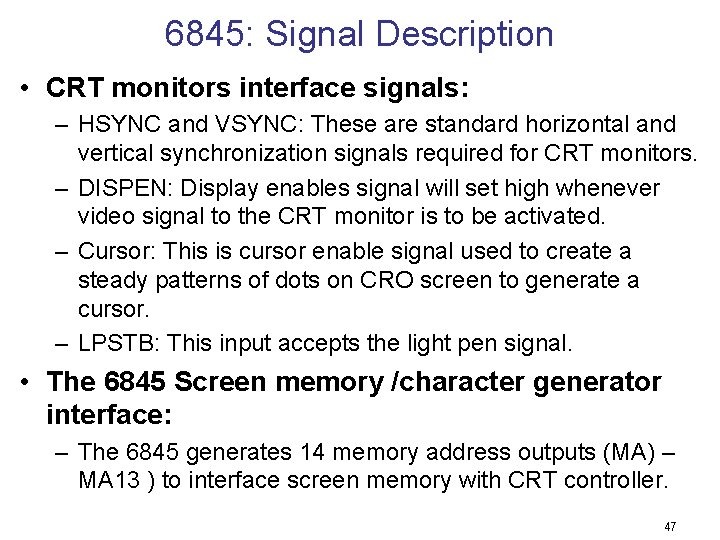
6845: Signal Description • CRT monitors interface signals: – HSYNC and VSYNC: These are standard horizontal and vertical synchronization signals required for CRT monitors. – DISPEN: Display enables signal will set high whenever video signal to the CRT monitor is to be activated. – Cursor: This is cursor enable signal used to create a steady patterns of dots on CRO screen to generate a cursor. – LPSTB: This input accepts the light pen signal. • The 6845 Screen memory /character generator interface: – The 6845 generates 14 memory address outputs (MA) – MA 13 ) to interface screen memory with CRT controller. 47

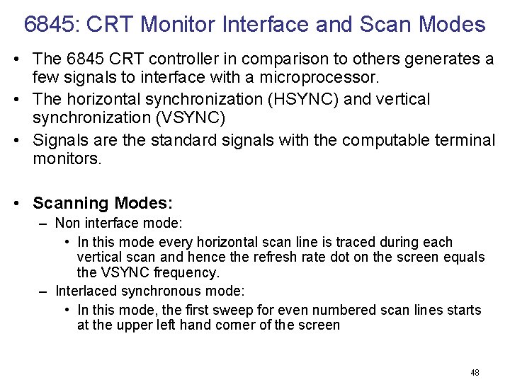
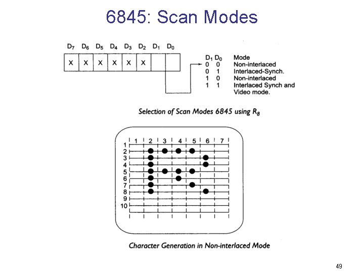
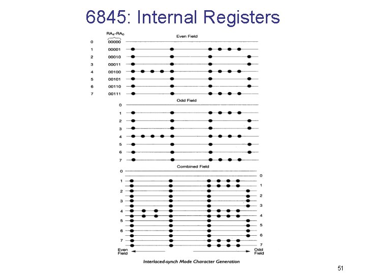
6845: CRT Monitor Interface and Scan Modes • The 6845 CRT controller in comparison to others generates a few signals to interface with a microprocessor. • The horizontal synchronization (HSYNC) and vertical synchronization (VSYNC) • Signals are the standard signals with the computable terminal monitors. • Scanning Modes: – Non interface mode: • In this mode every horizontal scan line is traced during each vertical scan and hence the refresh rate dot on the screen equals the VSYNC frequency. – Interlaced synchronous mode: • In this mode, the first sweep for even numbered scan lines starts at the upper left hand corner of the screen 48

6845: Scan Modes 49

6845: Interfacing With Different Entities 50

6845: Internal Registers 51

6845: Internal Registers • Internal registers of 6845 can be classified in to 3 groups as given below: – Horizontal format and timing registers – Vertical format and timing registers – Other special purpose registers • Horizontal format and timing registers: – The registers R 0, R 1, R 2 and R 3 can be programmed to control the Horizontal format and timing of the display. – Once loaded with the required parameters these not changed thereafter. • Vertical format and timing registers: – The registers R 4, R 5, R 6, R 7, R 8 and R 9 can be programmed to establish the vertical format and the related timings 52

6845: Internal Registers • Cursor position registers R 10 and R 11 – These registers R 10 and R 11 are known as cursor start register (R 10 )and cursor stop registers( R 11) respectively are used to determine the shape, type and position of the cursor • Primary operating registers – The registers R 12 to R 17 are known as Primary operating registers as they may be frequently accessed and updated during the system operation. – These six registers are arranged as three 14 -bit registers. 53

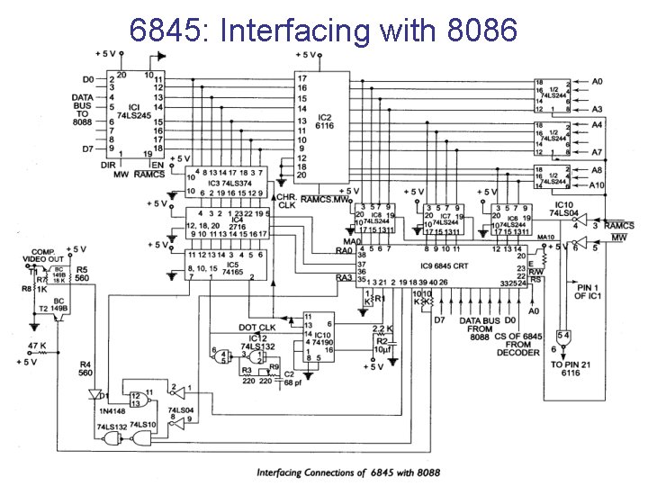
6845: Interfacing with 8086 54