DLD DIGITAL LOGIC DESIGN Dr Krishnanaik Vankdoth B
, M. Tech (ECE), Ph.")
DLD - DIGITAL LOGIC DESIGN Dr. Krishnanaik Vankdoth B. E(ECE), M. Tech (ECE), Ph. D (ECE) Professor in ECE Dept Vaagdevi college of Engineering Warangal – 506001 krishnanaik. ece@gmail. com 1

Books 1. “ Digital Design” By M. Morris Mano and Michael D. Ciletti 2. Logical Design and Application By Dr. Krishnanaik Vankdoth LAP LAMBERT Academic Publishing Dnfscland/Germany – 2014 3. Complementary Material “ Logic and Computer Design Fundamentals ” By M. Morris Mano & Charles R Kime. 2

DLD - DIGITAL LOGIC DESIGN Digital Systems and Binary Numbers Dr. V. Krishnanaik Ph. D 3

• Digital • Concerned with the interconnection among digital components and modules » Best Digital System example is General Purpose Computer • Logic Design • Deals with the basic concepts and tools used to design digital hardware consisting of logic circuits » Circuits to perform arithmetic operations (+, -, x, ÷) 4

• Digital Signal : Decimal values are difficult to represent in electrical systems. It is easier to use two voltage values than ten. • Digital Signals have two basic states: 1 (logic “high”, or H, or “on”) 0 (logic “low”, or L, or “off”) • Digital values are in a binary format. Binary means 2 states. • A good example of binary is a light (only on or off) on off Power switches have labels “ 1” for on and “ 0” for off. 5

• Bits and Pieces of DLD History • George Boole • Mathematical Analysis of Logic (1847) • An Investigation of Laws of Thoughts; Mathematical Theories of Logic and Probabilities (1854) • Claude Shannon • Rediscovered the Boole • “ A Symbolic Analysis of Relay and Switching Circuits “ • Boolean Logic and Boolean Algebra were Applied to Digital Circuitry ----- Beginning of the Digital Age and/or Computer Age World War II Computers as Calculating Machines Arlington (State Machines) “ Control “ 6

Motivation • Microprocessors/Microelectronics have revolutionized our world – Cell phones, internet, rapid advances in medicine, etc. • The semiconductor industry has grown tremendously 7

Digital Systems and Binary Numbers Digital age and information age Digital computers – General purposes – Many scientific, industrial and commercial applications • Digital systems – – Telephone switching exchanges Digital camera Electronic calculators, PDA's Digital TV • Discrete information-processing systems – Manipulate discrete elements of information – For example, {1, 2, 3, …} and {A, B, C, …}… 8

Analog and Digital Signal • Analog system – The physical quantities or signals may vary continuously over a specified range. • Digital system – The. X(t) physical quantities or signals can assume only X(t) discrete values. – Greater accuracy t Analog signal t Digital signal 9

10

Binary Digital Signal • An information variable represented by physical quantity. • For digital systems, the variable takes on discrete values. – Two level, or binary values are the most prevalent values. • Binary values are represented abstractly by: – – Digits 0 and 1 Words (symbols) False (F) and True (T) Words (symbols) Low (L) and High (H) And words On and Off V(t) • Binary values are represented by values or ranges of values of physical quantities. Logic 1 undefine Logic 0 t Binary digital signal 11
 = 10 – 10 digits {")
Decimal Number System • Base (also called radix) = 10 – 10 digits { 0, 1, 2, 3, 4, 5, 6, 7, 8, 9 } • Digit Position – Integer & fraction • Digit Weight – Weight = (Base) Position • Magnitude – Sum of “Digit x Weight” • Formal Notation 2 1 0 -1 -2 5 1 2 7 4 100 10 1 0. 01 10 2 0. 7 500 0. 04 d 2*B 2+d 1*B 1+d 0*B 0+d-1*B-1+d-2*B-2 (512. 74)10 12

• Base = 8 Octal Number System – 8 digits { 0, 1, 2, 3, 4, 5, 6, 7 } • Weights – Weight = (Base) Position • Magnitude – Sum of “Digit x Weight” • Formal Notation 64 8 1 1/8 1/64 5 1 2 7 4 2 1 0 -1 -2 5 *82+1 *81+2 *80+7 *8 -1+4 *8 -2 =(330. 9375)10 (512. 74)8 13

• Base = 2 Binary Number System – 2 digits { 0, 1 }, called binary digits or “bits” • Weights – Weight = (Base) Position • Magnitude – Sum of “Bit x Weight” • Formal Notation • Groups of bits 4 bits = Nibble 8 bits = Byte 4 2 1 1/2 1/4 1 0 1 2 1 0 -1 -2 1 *22+0 *21+1 *20+0 *2 -1+1 *2 -2 =(5. 25)10 (101. 01)2 1011 11000101 14

Hexadecimal Number System • Base = 16 – 16 digits { 0, 1, 2, 3, 4, 5, 6, 7, 8, 9, A, B, C, D, E, F } • Weights – Weight = (Base) Position • Magnitude – Sum of “Digit x Weight” • Formal Notation 256 16 1 1 E 5 7 A 2 1 0 -1 -2 1/16 1/256 1 *162+14 *161+5 *160+7 *16 -1+10 *16 -2 =(485. 4765625)10 (1 E 5. 7 A)16 15

The Power of 2 n 2 n 0 20=1 8 28=256 1 21=2 9 29=512 2 22=4 10 210=1024 3 23=8 11 211=2048 4 24=16 12 212=4096 5 25=32 20 220=1 M Mega 6 26=64 30 230=1 G Giga 7 27=128 40 240=1 T Tera Kilo 16

Addition • Decimal Addition 1 + 1 1 Carry 5 5 1 0 = Ten ≥ Base Subtract a Base 17

Binary Addition • Column Addition 1 1 1 1 1 0 1 = 61 1 0 1 1 1 = 23 1 0 0 = 84 + 1 0 ≥ (2)10 18

Binary Subtraction • Borrow a “Base” when needed 0 1 2 2 0 0 2 1 0 0 1 1 0 1 = 77 1 0 1 1 1 = 23 1 0 1 1 0 = 54 − 0 1 2 = (10)2 19

Binary Multiplication • Bit by bit 1 0 1 0 0 0 1 0 1 1 1 0 0 0 1 1 1 1 0 0 x 1 1 0 20
 Evaluate Magnitude Decimal (Base 10) Binary")
Number Base Conversions Evaluate Magnitude Octal (Base 8) Evaluate Magnitude Decimal (Base 10) Binary (Base 2) Hexadecimal (Base 16) Evaluate Magnitude 21
 to Binary Conversion • Divide the number by the ‘Base’ (=2) •")
Decimal (Integer) to Binary Conversion • Divide the number by the ‘Base’ (=2) • Take the remainder (either 0 or 1) as a coefficient • Take the quotient and repeat the division Example: (13)10 13 / 2 = 6 /2= 3 /2= 1 /2= Quotient Remainder 6 3 1 0 1 1 Answer: Coefficient a 0 = 1 a 1 = 0 a 2 = 1 a 3 = 1 (13)10 = (a 3 a 2 a 1 a 0)2 = (1101)2 MSB LSB 22
 to Binary Conversion • Multiply the number by the ‘Base’ (=2) •")
Decimal (Fraction) to Binary Conversion • Multiply the number by the ‘Base’ (=2) • Take the integer (either 0 or 1) as a coefficient • Take the resultant fraction and repeat the division Example: (0. 625)10 0. 625 * 2 = 0. 5 *2= Answer: Integer 1 0 1 Fraction . . . 25 5 0 Coefficient a-1 = 1 a-2 = 0 a-3 = 1 (0. 625)10 = (0. a-1 a-2 a-3)2 = (0. 101)2 MSB LSB 23
10 Quotient 175 / 8 = 21 / 8")
Decimal to Octal Conversion Example: (175)10 Quotient 175 / 8 = 21 / 8 = 2 /8= Remainder 21 2 0 Answer: 7 5 2 Coefficient a 0 = 7 a 1 = 5 a 2 = 2 (175)10 = (a 2 a 1 a 0)8 = (257)8 Example: (0. 3125)10 Integer 0. 3125 * 8 = 2 0. 5 *8= 4 Answer: Fraction . . 5 0 Coefficient a-1 = 2 a-2 = 4 (0. 3125)10 = (0. a-1 a-2 a-3)8 = (0. 24)8 24

Binary − Octal Conversion 23 • 8= • Each group of 3 bits represents an octal digit Assume Zeros Example: ( 1 0 1 1 0. 0 1 )2 ( 2 6 . 2 )8 Octal Binary 0 000 1 001 2 010 3 011 4 100 5 101 6 110 7 111 Works both ways (Binary to Octal & Octal to Binary) 25

Binary − Hexadecimal Conversion • 16 = 24 • Each group of 4 bits represents a hexadecimal digit Assume Zeros Example: ( 1 0 1 1 0. 0 1 )2 (1 6 . 4 )16 Hex Binary 0 1 2 3 4 5 6 7 8 9 A B C D E F 0000 0001 0010 0011 0100 0101 0110 0111 1000 1001 1010 1011 1100 1101 1110 1111 Works both ways (Binary to Hex & Hex to Binary) 26

Octal − Hexadecimal Conversion • Convert to Binary as an intermediate step Example: ( 2 6 . 2 )8 Assume Zeros ( 0 1 1 0. 0 1 0 )2 (1 6 . 4 )16 Works both ways (Octal to Hex & Hex to Octal) 27

Decimal, Binary, Octal and Hexadecimal Decimal Binary Octal Hex 00 01 02 03 04 05 06 07 08 09 10 11 12 13 14 15 0000 0001 0010 0011 0100 0101 0110 0111 1000 1001 1010 1011 1100 1101 1110 1111 00 01 02 03 04 05 06 07 10 11 12 13 14 15 16 17 0 1 2 3 4 5 6 7 8 9 A B C D E F 28

1. 5 Complements • • There are two types of complements for each base-r system: the radix complement and diminished radix complement. Diminished Radix Complement - (r-1)’s Complement – Given a number N in base r having n digits, the (r– 1)’s complement of N is defined as: (rn – 1) – N • • • Example for 6 -digit decimal numbers: – 9’s complement is (rn – 1)–N = (106– 1)–N = 999999–N – 9’s complement of 546700 is 999999– 546700 = 453299 Example for 7 -digit binary numbers: – 1’s complement is (rn – 1) – N = (27– 1)–N = 1111111–N – 1’s complement of 1011000 is 1111111– 1011000 = 0100111 Observation: – Subtraction from (rn – 1) will never require a borrow – Diminished radix complement can be computed digit-by-digit – For binary: 1 – 0 = 1 and 1 – 1 = 0 29
 – All ‘ 0’s become ‘ 1’s")
Complements • 1’s Complement (Diminished Radix Complement) – All ‘ 0’s become ‘ 1’s – All ‘ 1’s become ‘ 0’s Example (10110000)2 (01001111)2 If you add a number and its 1’s complement … 10110000 + 01001111 30

Complements • Radix Complement The r's complement of an n-digit number N in base r is defined as rn – N for N ≠ 0 and as 0 for N = 0. Comparing with the (r 1) 's complement, we note that the r's complement is obtained by adding 1 to the (r 1) 's complement, since rn – N = [(rn 1) – N] + 1. • Example: Base-10 The 10's complement of 012398 is 987602 The 10's complement of 246700 is 753300 • Example: Base-2 The 2's complement of 1101100 is 0010100 The 2's complement of 0110111 is 1001001 31
 – Take 1’s complement then add 1 OR")
Complements • 2’s Complement (Radix Complement) – Take 1’s complement then add 1 OR – Toggle all bits to the left of the first ‘ 1’ from the right Example: Number: 10110000 1’s Comp. : 01001111 + 1 01010000 32

Complements • Subtraction with Complements – The subtraction of two n-digit unsigned numbers M – N in base r can be done as follows: 33

Complements • Example 1. 5 – Using 10's complement, subtract 72532 – 3250. • Example 1. 6 – Using 10's complement, subtract 3250 – 72532. There is no end carry. Therefore, the answer is – (10's complement of 30718) = 69282. 34

Complements • Example 1. 7 – Given the two binary numbers X = 1010100 and Y = 1000011, perform the subtraction (a) X – Y ; and (b) Y X, by using 2's complement. There is no end carry. Therefore, the answer is Y – X = (2's complement of 1101111) = 0010001. 35

Complements • Subtraction of unsigned numbers can also be done by means of the (r 1)'s complement. Remember that the (r 1) 's complement is one less then the r's complement. • Example 1. 8 – Repeat Example 1. 7, but this time using 1's complement. There is no end carry, Therefore, the answer is Y – X = (1's complement of 1101110) = 0010001. 36

1. 6 Signed Binary Numbers • To represent negative integers, we need a notation for negative values. • It is customary to represent the sign with a bit placed in the leftmost position of the number since binary digits. • The convention is to make the sign bit 0 for positive and 1 for negative. • Example: • Table 1. 3 lists all possible four-bit signed binary numbers in the three representations. 37

Signed Binary Numbers 38

Signed Binary Numbers • Arithmetic addition – The addition of two numbers in the signed-magnitude system follows the rules of ordinary arithmetic. If the signs are the same, we add the two magnitudes and give the sum the common sign. If the signs are different, we subtract the smaller magnitude from the larger and give the difference the sign if the larger magnitude. – The addition of two signed binary numbers with negative numbers represented in signed-2's-complement form is obtained from the addition of the two numbers, including their sign bits. – A carry out of the sign-bit position is discarded. • Example: 39

Signed Binary Numbers • Arithmetic Subtraction – In form: 1. 2’s-complement Take the 2’s complement of the subtrahend (including the sign bit) and 2. add it to the minuend (including sign bit). A carry out of sign-bit position is discarded. ( 6) ( 13) (11111010 11110011) • Example: (11111010 + 00001101) 00000111 (+ 7) 40

1. 7 Binary Codes Digital data is represented, stored and transmitted as groups of binary digits also known as binary code. Weighted codes: In weighted codes, each digit is assigned a specific weight according to its position. Non-weighted codes: In non-weighted codes are not appositionally weighted. Reflective codes: A code is reflective when the code is self complementing. In other words, when the code for 9 is the complement the code for 0, 8 for 1, 7 for 2, 6 for 3 and 5 for 4. Sequential codes: In sequential codes, each succeeding 'code is one binary number greater than its preceding code. Alphanumeric codes: Codes used to represent numbers, alphabetic characters, symbols Error defecting and correcting codes: Codes which allow error defection and correction are called error detecting and' correcting codes. 41

• BCD Code – A number with k decimal digits will require 4 k bits in BCD. – Decimal 396 is represented in BCD with 12 bits as 0011 1001 0110, with each group of 4 bits representing one decimal digit. – A decimal number in BCD is the same as its equivalent binary number only when the number is between 0 and 9. – The binary combinations 1010 through 1111 are not used and have no meaning in BCD. Example: Consider decimal 185 and its corresponding value in BCD and binary: BCD addition 42

Binary Codes • Other Decimal Codes 43

Binary Codes • Gray Code – The advantage is that only bit in the code group changes in going from one number to the next. • Error detection. • Representation of analog data. 001 • Low 000 power design. 010 011 100 110 1 -1 and onto!! 111 44
 Character Code 45")
• American Standard Code for Information Interchange (ASCII) Character Code 45

• ASCII Character Code 46

ASCII Character Codes and Properties • American Standard Code for Information Interchange (Refer to Table 1. 7) • A popular code used to represent information sent as character-based data. • It uses 7 -bits to represent: – 94 Graphic printing characters. – 34 Non-printing characters. • Some non-printing characters are used for text format (e. g. BS = Backspace, CR = carriage return). • Other non-printing characters are used for record marking and flow control (e. g. STX and ETX start and end text areas). • ASCII has some interesting properties: – Digits 0 to 9 span Hexadecimal values 3016 to 3916 – Upper case A-Z span 4116 to 5 A 16 – Lower case a-z span 6116 to 7 A 16 • Lower to upper case translation (and vice versa) occurs by flipping bit 6. 47

• Error-Detecting Code – To detect errors in data communication and processing, an eighth bit is sometimes added to the ASCII character to indicate its parity. – A parity bit is an extra bit included with a message to make the total number of 1's either even or odd. • Example: – Consider the following two characters and their even and odd parity: 48
, in the form of")
• Error-Detecting Code – Redundancy (e. g. extra information), in the form of extra bits, can be incorporated into binary code words to detect and correct errors. – A simple form of redundancy is parity, an extra bit appended onto the code word to make the number of 1’s odd or even. Parity can detect all single-bit errors and some multiple-bit errors. – A code word has even parity if the number of 1’s in the code word is even. – A code word has odd parity if the number of 1’s in the code word is odd. – Example: Message A: 10001001 1 (even parity) Message B: 10001001 0 (odd parity) 49

Hamming Codes • • Invented W. B Hamming and Simple 1 parity bit can tell us an error occurred Multiple parity bits can also tell us where it occurred O(lg(n)) bits needed to detect and correct one bit errors. In generally we use 7 bits hamming code – 4 data bits/message bit (m) and 3 parity bits (2 P>= P+m+1) Example: Byte 1011 0001 Two data blocks, 1011 and 0001. Expand the first block to 7 bits: _ _ 1 Bit 1 is 0, because b 3+b 5+b 7 is even. Bit 2 is 1, b 3+b 6+b 7 is odd. bit 4 is 0, because b 5+b 6+b 7 is even. Our 7 bit block is: 0 1 1 0 0 1 1 _ 0 1 1. Repeat for right block giving 1 101001 Error detectings: 0 1 1 1 Re-Check each parity bit Bits 1 and 4 are incorrect 1 + 4 = 5, so the error occurred in bit 5 Dr. V. Krishnanaik Ph. D 50

Binary Storage and Registers • Registers – A binary cell is a device that possesses two stable states and is capable of storing one of the two states. – A register is a group of binary cells. A register with n cells can store any discrete quantity of information that contains n bits. n cells • A binary cell • A register • Register Transfer 2 n possible states – Two stable state – Store one bit of information – Examples: flip-flop circuits, ferrite cores, capacitor – A group of binary cells – AX in x 86 CPU – A transfer of the information stored in one register to another. – One of the major operations in digital system. – An example in next slides. 51

A Digital Computer Example Outputs: CRT, LCD, modem, speakers Inputs: Keyboard, mouse, modem, microphone Synchronous or Asynchronous? 52

Transfer of information Figure 1. 1 Transfer of information among register 53

Transfer of information • The other major component of a digital system – Circuit elements to manipulate individual bits of information – Load-store machine LD LD ADD SD Figure 1. 2 Example of binary information processing R 1; R 2; R 3, R 2, R 1; R 3; 54

Binary Logic • Definition of Binary Logic – Binary logic consists of binary variables and a set of logical operations. – The variables are designated by letters of the alphabet, such as A, B, C, x, y, z, etc, with each variable having two and only two distinct possible values: 1 and 0, – Three basic logical operations: AND, OR, and NOT. 55

Binary Logic gates • Truth Tables, Boolean Expressions, and Logic Gates AND OR NOT x y z x z 0 0 0 0 1 1 1 0 0 1 1 1 1 z=x • y=xy z=x+y z = x’
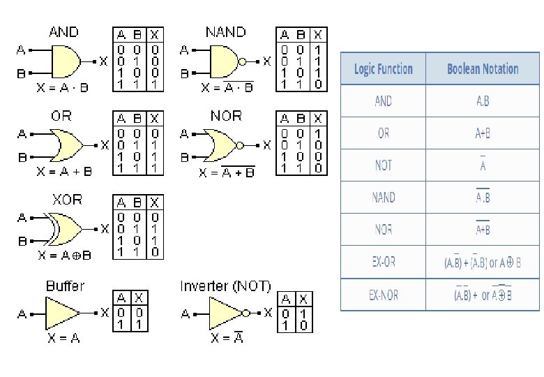

Universal Gate • NAND and NOR Gates are called Universal Gates because AND, OR and NOT gates can be implemented &created by using these gates. NAND Gate Implementations NOR Gate Implementations Dr. V. Krishnanaik Ph. D

Binary Logic • Logic gates – Example of binary signals 3 Logic 1 2 Un-define 1 0 Logic 0 Figure 1. 3 Example of binary signals 59

Binary Logic • Logic gates – Graphic Symbols and Input-Output Signals for Logic gates: Fig. 1. 4 Symbols for digital logic circuits Fig. 1. 5 Input-Output signals for gates 60

Binary Logic • Logic gates – Graphic Symbols and Input-Output Signals for Logic gates: Fig. 1. 6 Gates with multiple inputs 61
, 1854 Invented by George Boole in 1854 An")
Boolean Algebra : George Boole(English mathematician), 1854 Invented by George Boole in 1854 An algebraic structure defined by a set B = {0, 1}, together with two binary operators (+ and ·) and a unary operator ( ) “An Investigation of the Laws of Thought, on Which Are Founded the Mathematical Theories of Logic and Probabilities” Boolean Algebra {(1, 0), Var, (NOT, AND, OR), Thms} q. Mathematical tool to expression and analyze digital (logic) circuits q. Claude Shannon, the first to apply Boole’s work, 1938 – “A q. This Symbolic Analysis of Relay and Switching Circuits” at MIT chapter covers Boolean algebra, Boolean expression and its evaluation and simplification, and VHDL program 62
 :")
Basic Functions and Basic Functions Boolean functions : NOT, AND, OR, exclusive OR(XOR) : odd function exclusive NOR(XNOR) : even function(equivalence) Basic functions • AND Z=X Y or Z=XY Z=1 if and only if X=1 and Y=1, otherwise Z=0 • OR Z=X + Y Z=1 if X=1 or if Y=1, or both X=1 and Y=1. Z=0 if and only if X=0 and Y=0 • NOT Z=X or Z=1 if X=0, Z=0 if X=1 63

64
")
Boolean Operations and Expressions • Boolean Addition – Logical OR operation Ex 4 -1) Determine the values of A, B, C, and D that make the sum term A+B’+C+D’ Sol) all literals must be ‘ 0’ for the sum term to be ‘ 0’ A+B’+C+D’=0+1’+0+1’=0 A=0, B=1, C=0, and D=1 • Boolean Multiplication – Logical AND operation Ex 4 -2) Determine the values of A, B, C, and D for AB’CD’=1 Sol) all literals must be ‘ 1’ for the product term to be ‘ 1’ AB’CD’=10’ 10’=1 A=1, B=0, C=1, and D=0 65

Basic Identities of Boolean Algebra The relationship between a single variable X, its complement X , and the binary constants 0 and 1 66

Laws of Boolean Algebra • Commutative Law: the order of literals does not matter A+B=B+A AB=BA • Associative Law: the grouping of literals does not matter A + (B + C) = (A + B) + C (=A+B+C) Distributive Law : A(B + C) = AB + AC 67 A(BC) = (AB)C (=ABC) (A+B)(C+D) = AC + AD + BC + BD

Rules of Boolean Algebra A+0=A In math if you add 0 you have changed nothing in Boolean Algebra ORing with 0 changes nothing A • 0=0 In math if 0 is multiplied with anything you get 0. If you AND anything with 0 you get 0 A • 1 =A ANDing anything with 1 will yield the anything A+A = A ORing with itself will give the same result A+A’=1 Either A or A’ must be 1 so A + A’ =1 A • A = A ANDing with itself will give the same result A • A’ =0 In digital Logic 1’ =0 and 0’ =1, so AA’=0 since one of the inputs must be 0. 68 A = (A’)’ If you not something twice you are back to the beginning

A + A’B = A + B If A is 1 the output is 1 If A is 0 the output is B A + AB = A (A + B)(A + C) = A + BC • De. Morgan’s Theorem – F (A, A , , + , 1, 0) = F(A , A, + , , 0, 1) (A • B)’ = A’ + B’ and (A + B)’ = A’ • B’ – De. Morgan’s theorem will help to simplify digital circuits using NORs and NANDs his theorem states – 69

Boolean Analysis of Logic Circuits • Constructing a Truth Table for a Logic Circuit – Convert the expression into the min-terms containing all the input literals – Get the numbers from the min-terms – Putting ‘ 1’s in the rows corresponding to the min-terms and ‘ 0’s in the remains Ex) A(B+CD)=AB(C+C’) (D+D’) +A(B+B’)CD =ABC(D+D’) +ABC’(D+D’) +ABCD+AB’CD =ABCD+ABCD’+ABC’D+ABC’D’ +AB’CD =m 11+m 12+m 13+m 14+m 15= (11, 12, 13, 14, 15) A(B+CD) = m 11+m 12+m 13+m 14+m 15 = (11, 12, 13, 14, 15) 70
 Form Ex) AB+ABC, ABC+CDE+B’CD’ q. The")
Standard Forms of Boolean Expressions q. The Sum-of-Products(SOP) Form Ex) AB+ABC, ABC+CDE+B’CD’ q. The Product-of-Sums(POS) Form Ex) (A+B)(A+B+C), (A+B+C)(C+D+E)(B’+C+D’) q. Principle of Duality : SOP POS q. Domain of a Boolean Expression : The set of variables contained in the expression Ex) A’B+AB’C : the domain is {A, B, C} Standard SOP Form (Canonical SOP Form) – For all the missing variables, apply (x+x’)=1 to the AND terms of the expression – List all the min-terms in forms of the complete set of variables in ascending order Ex : Convert the following expression into standard SOP form: AB’C+A’B’+ABC’D Sol) domain={A, B, C, D}, AB’C(D’+D)+A’B’(C’+C)(D’+D)+ABC’D =AB’CD’+AB’CD+A’B’C’D’+A’B’C’D+A’B’CD’+A’B’CD+ABC’D =1010+1011+0000+0001+0010+0011+1101 =0+1+2+3+10+11+13 = (0, 1, 2, 3, 10, 11, 13) 71
 – For all the missing variables, apply (x’x)=0")
Standard POS Form (Canonical POS Form) – For all the missing variables, apply (x’x)=0 to the OR terms of the expression – List all the max-terms in forms of the complete set of variables in ascending order Ex : Convert the following expression into standard POS form: (A+B’+C)(B’+C+D’)(A+B’+C’+D) Sol) domain={A, B, C, D}, (A+B’+C)(B’+C+D’)(A+B’+C’+D) =(A+B’+C+D’D)(A’A+B’+C+D’)(A+B’+C’+D) =(A+B’+C+D’)(A+B’+C+D)(A’+B’+C+D’)(A+B’+C’ +D)=(0100) )(0101)(0110)(1101)= (4, 5, 6, 13) 72

Converting Standard SOP to Standard POS Step 1. Evaluate each product term in the SOP expression. Determine the binary numbers that represent the product terms Step 2. Determine all of the binary numbers not included in the evaluation in Step 1 Step 3. Write in equivalent sum term for each binary number Step 2 and expression in POS form Ex : Convert the following SOP to POS Sol) SOP= A’B’C’+A’BC+AB’C+ABC=0+2+3+5+7 = (0, 2, 3, 5, 7) POS=(1)(4)(6) = (1, 4, 6) (=(A+B+C’)(A’+B+C)(A’+B’+C)) SOP and POS Observations q – Canonical Forms (Sum-of-minterms, Product-of-Maxterms), or other standard forms (SOP, POS) differ in complexity – Boolean algebra can be used to manipulate equations into simpler forms – Simpler equations lead to simpler implementations 73

Summary of Minterms and Maxterms • There are 2 n minterms and maxterms for Boolean functions with n variables. • Minterms and maxterms are indexed from 0 to 2 n – 1 • Any Boolean function can be expressed as a logical sum of minterms and as a logical product of maxterms • The complement of a function contains those minterms not included in the original function • The complement of a sum-of-minterms is a product-of-maxterms with the same indices Dual of a Boolean Expression • To changing 0 to 1 and + operator to – vise versa for a given boolean function q Example: F = (A + C) · B + 0 dual F = (A · C + B) · 1 = A · C + B q Example: G = X · Y + (W + Z) dual G = Unless it happens to be self-dual, the dual of an expression does not equal the expression itself Are any of these functions self-dual? (A+B)(A+C)(B+C)=(A+BC)(B+C)=AB+AC+BC 74
 – Karnaugh map(map method)) XY+XY")
Karnaugh Map • Simplification methods – Boolean algebra(algebraic method) – Karnaugh map(map method)) XY+XY =X(Y+Y )=X – Quine-Mc. Cluskey(tabular method) – Three- and Four-input Kanaugh maps Gray code 75 Dr. V. Krishnanaik Ph. D
 Steps 1. 2. 3. Sketch a Karnaugh map grid for")
Karnaugh Map (K- Map) Steps 1. 2. 3. Sketch a Karnaugh map grid for the given problem. in power of 2 N Squares Fill in the 1’s and 0’s from the truth table of sop or pos Boolean function Circle groups of 1’s. w w 4. Circle the largest groups of 2, 4, 8, etc. first. Minimize the number of circles but make sure that every 1 is in a circle. Write an equation using these circles. Example) F(X, Y, Z)= m(2, 3, 4, 5) =X Y+XY 76 Example) F(X, Y, Z)= m(0, 2, 4, 6) = X Z +XZ =Z (X +X)=Z

Four-Variable K-Map : 16 minterms : m 0 ~ m 15 Rectangle group – 2 -squares(minterms) : 3 -literals product term – 4 -squares : 2 -literals product term – 8 -squares : 1 -literals product term – 16 -squares : logic 1 77
= m(0, 2, 7, 8, 9, 10, 11) = WX’ +")
F(W, X, Y, Z)= m(0, 2, 7, 8, 9, 10, 11) = WX’ + X’Z’ + W’XYZ Ex 4 -28) Minimize the following expression AB’C+A’B’C+A’B’C’+AB’C’ Sol) B’+A’C 78
 D’+B’C q. Don’t Care Conditions •")
Ex Minimize the following expression B’C’D’+A’BC’D’+A’B’CD+A’B’CD’+A’BCD’ +ABCD’+AB’CD’ Sol) D’+B’C q. Don’t Care Conditions • it really does not matter since they will never occur(its output is either ‘ 0’ or ‘ 1’) • The don’t care terms can be used to advantage on the Karnaugh map 79
(A+B+C’+D)(A’+B+C+D’)(A+B’+C+D)(A’+B’+C+D) Sol) (B+C+D)=(A’A+B+C+D)=(A’+B+C+D)(A+B+C+D) (1+0+0+0)(0+0+1+0) (1+0+0+1)(0+1+0+0)(1+1+0+0) F=(C+D)(A’+B+C)(A+B+D) q Converting Between")
Ex K- Map for POS (B+C+D)(A+B+C’+D)(A’+B+C+D’)(A+B’+C+D)(A’+B’+C+D) Sol) (B+C+D)=(A’A+B+C+D)=(A’+B+C+D)(A+B+C+D) (1+0+0+0)(0+0+1+0) (1+0+0+1)(0+1+0+0)(1+1+0+0) F=(C+D)(A’+B+C)(A+B+D) q Converting Between POS and SOP Using the K-map Ex 4 -33) (A’+B’+C+D)(A+B’+C+D) (A+B+C+D’)(A+B+C’+D’) (A’+B+C+D’) (A+B+C’+D) 80

81

Quine-Mc. Cluskey - Tabular Method • Step 1 − Arrange the given min terms in an ascending order and make the groups based on the number of ones present in their binary representations. - ‘n+1’ groups • Step 2 − Compare the min terms present in successive groups. If there is a change in only one-bit position, then take the pair of those two min terms. Place this symbol ‘_’ in the differed bit position and keep the remaining bits as it is. • Step 3 − Repeat step 2 with newly formed terms till we get all prime implicants. • Step 4 − Formulate the prime implicant table. It consists of set of rows and columns. Place ‘ 1’ in the cells corresponding to the min terms that are covered in each prime implicant. • Step 5 − Find the essential prime implicates by observing each column. Those essential prime implicants will be part of the simplified Boolean function. • Step 6 − Reduce the prime implicant table by removing the row of each essential prime implicant and the columns corresponding to the min terms that are covered in that essential prime implicant. Repeat step 5 for Reduced prime implicant table. Stop this process when all min terms of given Boolean function are over. 82

83

84

Digital Circuits • Digital circuits are two types 1. Combinational circuit consists of logic gates whose outputs at any time are determined directly from the present combination of inputs without regard to previous inputs. 2. Sequential Circuit employ memory elements in addition to logic gates. Their outputs are a function of the inputs and the state of the memory elements. Dr. V. Krishnanaik Ph. D 85

Combinational Logic circuits for digital systems may be combinational or sequential. A combinational circuit consists of input variables, logic gates, and output variables. Hence, a combinational circuit can be described by: 1. A truth table that lists the output values for each combination of the input variables, or 2. m Boolean functions, one for each output variable. Combinational vs. Sequential Circuits Combinational circuits are memory-less. Thus, the output value depends ONLY on the current input values. Sequential circuits consist of combinational logic as well as memory elements (used to store certain circuit states). Outputs depend on BOTH current input values and previous input values (kept in the storage elements). Design Procedure Given a problem statement: ● Determine the number of inputs and outputs Dept. of Computer Science And Applications, SJCET, Palai Page 46

7 ●Derive the truth table ●Simplify the Boolean expression for each output ●Produce the required circuit Half Adder : A combinational circuit that performs the addition of two bits is called a half adder, We need two input and outputs The truth table for the half adder is listed below: xy C S 00 0 0 01 0 1 10 0 1 11 S(x, y) = x’y + xy’ Dept. of Computer Science And Applications, SJCET, Palai 1 0 C(x, y) = xy Page 47

Full Adder : One that performs the addition of three bits (two significant bits and a previous carry) is a full adder. x yz C S 0 00 0 01 0 10 0 1 0 11 1 00 0 1 10 1 11 1 1 S = x’y’z + x’yz’ + xy’z’ + xyz Alternative formulae using algebraic manipulation: C = X. Y + X. Z + Y. Z = X. Y + (X + Y). Z = X. Y + ((X XOR Y) + X. Y). Z = X. Y + (X XOR Y). Z + X. Y. Z = X. Y + (X XOR Y). Z C = xy + xz + yz

S = X'. Y'. Z + X'. Y. Z' + X. Y'. Z' + X. Y. Z = X‘. (Y'. Z + Y. Z') + X. (Y'. Z' + Y. Z) = X'. (Y XOR Z) + X. (Y XOR Z)' = X XOR (Y XOR Z) or (X XOR Y) XOR Z Full adder using two half adder Parallel Binary Adders • Parallel Adder is a digital circuit that produces the arithmetic sum of 2 binary numbers. • Constructed with full adders connected in cascade, with output carry from each full adder connected to the input carry of next full adder in the chain. • The carries are connected in a chain through the full adders. • Two methods to handle carries in parallel adder 1. Ripple carry: carry out of each FA is connected to the carry input of next FA 2. Carry Look ahead: it anticipates the output carry of each stage, and based on the input bits of each stage, produces the output carry by either carry generation or carry propagation.

Carry generation: output carry is produced internally by the FA. carry is generated only when both input bits are 1 s. the generated carry C is expressed as the AND function of two input bits A and B so C=AB. Carry propagation: occurs when the i/p carry is rippled to become the o/p carry. an i/p carrymay be propagated by the full adder when either or both of the i/p bits are 1 s. the propagated carry Cp is expressed as the OR function of the i/p bits ie Cp=A+B 2 - Bit Parallel Adder • • LSB of two binary numbers are represented by A 1 and B 1. The next higher bit are A 2 and B 2. The resulting 1 2 and CO, in which the CO becomes MSB. The carry output CO of each adder is connected as the carry input of the next higher order. A 2 A 1 + B 2 B 1 2 C 0 ∑ ∑ 1 Fig : bit adder using two full adder Four Bit Parallel Adders • An n-bit adder requires n full adders with each output connected to the input carry of the next higher-order full adder. • The carry output of each adder is connected to the carry input of next adder called as internal carries.

Fig : bit adder The logic symbol for a 4 -bit parallel adder is shown. This 4 -bit adder includes a Carry In (labeled C 0) and a Carry Out (labeled C 4). Fig : Truth table for 4 bit parallel adder 74283 Four-bit binary adder 7483 is an older chip that is functionally identical to the 74283, but the pins are laid out differently Cascading Parallel Adders When we connect the outputs from one circuit to the inputs of another identical circuit to expand the number of bits being operated on, we say that the circuits are cascaded together. For example, you can cascade two 4 -bit parallel adders to add two 8 -bit numbers. To do this, connect the lower-order adder’s Carry Out to the higherorder adder’s Carry In.

MODULE 3 MCA-102 DIGITAL SYSTEMS & LOGIC DESIGN Fig : cascading of parallel adders Binary Subtraction • The subtraction A-B can be performed by taking the 2's complement of B and adding to A. • The 2's complement of B can be obtained by complementing B and adding one to the result. A-B = A + 2 C(B) = A + 1 C(B) + 1 = A + B’ + 1 Fig : binary substractor circuit Adder/Substractor Design requires: (i) XOR gates: ADMN 2014 -‘ 17
S connected")
MODULE 3 MCA-102 DIGITAL SYSTEMS & LOGIC DESIGN ADMN 2014 -‘ 17 (ii)S connected to carry-in. Fig : adder/substractor circuit • When S=0, the circuit performs A + B. The carry in is 0, and the XOR gates simply pass B untouched. • When S=1, the carry into the least significant bit (LSB) is 1, and B is complemented (1’s complement) prior to the addition; hence, the circuit adds to A the 1’s complement of B plus 1 (from the carry into the LSB). Magnitude Comparator : A magnitude comparator is a combinational circuit that compares two numbers, A and B, and then determines their relative magnitudes. A>B A=B A<B Problem: Design a magnitude comparator that compares 2 4 -bit numbers A and B and determines whether: A > B, or A = B, or A < B Inputs First n-bit number A and Second n-bit number B
, where: GT = 1 IFF A >")
Outputs: 3 output signals (GT, EQ, LT), where: GT = 1 IFF A > B EQ = 1 IFF A = B Exactly One of these 3 outputs equals 1, while the other 2 outputs are 0`s. Solution: Inputs: 8 -bits (A ⇒ 4 -bits, B ⇒ 4 -bits). A and B are two 4 -bit numbers. Let A = A 3 A 2 A 1 A 0, and Let B = B 3 B 2 B 1 B 0. Design of the EQ Define Xi = Ai xnor Bi = Ai Bi + Ai’ Bi’ Xi = 1 IFF Ai = Bi ∀ i =0, 1, 2 and 3 Xi = 0 IFF Ai ≠ Bi Therefore the condition for A = B or EQ=1 IFF A 3= B 3 → (X 3 = 1), and A 2= B 2 → (X 2 = 1), and A 1= B 1 → (X 1 = 1), and A 0= B 0 → (X 0 = 1). Thus, EQ=1 IFF X 3 X 2 X 1 X 0 = 1. In other words, EQ = X 3 X 2 X 1 X 0 Designing GT and LT: GT = 1 if A > B: If A 3 > B 3 3= 1 and B 3 = 0 If A 3 = B 3 and A 2 > B 2 If A 3 = B 3 and A 2 = B 2 and A 1 > A 1 If A 3 = B 3 and A 2 = B 2 and A 1 = B 1 and A 0 > B 0 Therefore, GT = A 3 B 3‘+ X 3 A 2 B 2‘+ X 3 X 2 A 1 B 1‘+ X 3 X 2 X 1 A 0 B 0‘ Similarly, LT = A 3’B 3 + X 3 A 2‘B 2 + X 3 X 2 A 1’B 1 + X 3 X 2 X 1 A 0’ B 0 LT = 1 IFF A < B

Fig : 4 bit magnitude comparator Decoder : A decoder is a logic circuit that accepts a set of inputs that represents a binary number and activates • A decoder has ------ N inputs and only the output that corresponds to the input number. 2 N outputs • Exactly one output will be active for each combination of the inputs. • Each of these input combinations only one of the M outputs will be active HIGH (1), all the other outputs are LOW (0). • An AND gate can be used as the basic decoding element because it produces a HIGH output only when all inputs are HIGH.

• If an active-LOW output (74138, one of the output will low and the rest will be high) is required for each decoded number, the entire decoder can be implemented with NAND gates Inverters • If an active-HIGH output (74139, one of the output will high and the rest will be low) is required for each decoded number, the entire decoder can be implemented with AND gates Inverters Decoder example : 2 -to-4 -Line Decoder fig : 2 -4 decoder with active high output Fig : logical symbol and truth table of 2 -4 decoder 3 line to 8 line decoder (active-HIGH) • It can be called a 3 -line-to- 8 -line decoder, because it has three input lines and eight output lines. • It could also be called a binary-octal decoder or converters because it takes a three bit binary input code and activates the one of the eight outputs corresponding to that code. It is also referred to as a 1 -of-8 decoder, because only 1 of the 8 outputs is activated at one time.

Application example A simplified computer I/O port system with a port address decoder with only four address lines shown.

Fig : peripheral decoding in computer • Computer must communicate with a variety of external devices called peripherals by sending and/or receiving data through what is known as input/output (I/O) ports • Each I/O port has a number, called an address, which uniquely identifies it. When the computer wants to communicate with a particular device, it issues the appropriate address code for the I/O port to which that particular device is connected. The binary port address is decoded and appropriate decoder output is activated to enable the I/O port • Binary data are transferred within the computer on a data bus, which is a set of parallel lines BCD -to- Decimal decoders • The BCD- to-decimal decoder converts each BCD code into one of Ten Positional decimal digit indications. It is frequently referred as a 4 -line -to- 10 line decoder • The method of implementation is that only ten decoding gates are required because the BCD code represents only the ten decimal digits 0 through 9. • Each of these decoding functions is implemented with NAND gates to provide active -LOW outputs. If an active HIGH output is required, AND gates are used for decoding

MODULE 3 MCA-102 DIGITAL SYSTEMS & LOGIC DESIGN ADMN 2014 -‘ 17 Fig : a. logic circuit for BCD to Decimal decoder b. logical symbol of BCD to Decimal decoder IC c. truth table BCD to 7 -Segment Display Decoder 1. Used to convert a BCD or a binary code into a 7 segment code used to operate a 7 segment LED display. 2. It generally has 4 input lines and 7 output lines. Here we design a simple display decoder circuit using logic gates. Fig : logical symbol of BCD-7 segment decoder Dept. of Computer Science And Applications, SJCET, Palai Page 59

Encoders typically have 2 N inputs and N outputs. These are called 2 N–to–N encoders. Encoders can also be devised to encode various symbols and alphabetic characters. The process of converting from familiar symbols or numbers to a coded format is called encoding. Fig : Logical diagram of Encoder 8 to-3 encoder Implementation Octal-to-Binary An octal to binary encoder has 2 3 = 8 input lines D 0 to D 7 and 3 output lines Y 0 to Y 2. Below is the truth table for an octal to binary encoder. Fig : Truth table for 8 -3 encoder From the truth table, the outputs can be expressed by following Boolean Function. Y 0 = D 1 + D 3 + D 5 + D 7

Y 1 = D 2 + D 3 + D 6 + D 7 Y 2 = D 4 + D 5 + D 6 + D 7 Note: Above boolean functions are formed by ORing all the input lines for which output is 1. For instance Y 0 is 1 for D 1, D 3, D 5, D 7 input lines. The encoder can therefore be implemented with OR gates whose inputs are determined directly from truth table as shown in the image below: Fig : logic circuit for 8 -3 encoder Decimal – BCD encoder • Encoder will produce a BCD output corresponding to the highest-order decimal digit input that is active and will ignore any other lower order active inputs. Fig : truth table for 10 -4 encoder -- From the truth table, the outputs can be expressed by following Boolean Function. Note: Below Boolean functions are formed by OR ing all the input lines for which output is 1. For instance A 0 is 1 for 1, 3, 5, 7 or 9 input lines. A 0 = 1+3+5+7+9

A 1 = 2+3+6+7 A 2 = 4+5+6+7 A 3 = 8+9 The decimal to bcd encoder can therefore be implemented with OR gates whose inputs are determined directly from truth table as shown in the image below. Fig : Logic circuit and symbol for 10 -4 encoder Multiplexer A multiplexer or mux is a device that selects one of several analog or digital input signals and forwards the selected input into a single line. A multiplexer of 2 n inputs has n select lines, which are used to select which input line to send to the output. ” The select lines determine which input is connected to the output. MUX Types 2 -to-1 (1 select line) 4 -to-1 (2 select lines) 8 -to-1 (3 select lines) 16 -to-1 (4 select lines)
 Fig : logic circuit, symbol")
Fig : multiplexer block diagram 4 to-1 Multiplexer (MUX) Fig : logic circuit, symbol and table for 4 -1 multiplexer The Boolean expression for this 4 -to-1 Multiplexer above with inputs D 0 to D 3 and data select lines A, B is given as: Y = A’B’D 0 + A’B D 1 + AB’D 2 + ABD 3 Demultiplexer • A DEMUX is a digital switch with a single input (source) and a multiple outputs (destinations). • The select lines determine which output the input is connected to. • DEMUX Types
 1 -to-4 (2 select lines) 1 -to-8 (3 select")
1 -to-2 (1 select line) 1 -to-4 (2 select lines) 1 -to-8 (3 select lines) 1 -to-16 (4 select lines) Fig : Demultiplexer circuit symbol 1 to-4 De-Multiplexer (DEMUX) Fig: logic circuit for 1 -4 demultiplexer, symbol and table Parity Bit Generator The most common error detection code used is the parity bit. A parity bit is an extra bit included with a binary message to make the total number of 1's either odd or even. A parity bit added to n-bit code produces (n+1)-bit code with an odd (or even) count of 1 s Odd Parity bit: count of 1 s in (n+1)-bit code is odd o So use an even function to generate the odd parity bit Even Parity bit: count of 1 s in (n+1)-bit code is even o So use an odd function to generate the even parity bit

To check for odd parity o Use an even function to check the (n+1)-bit code To check for even parity o Use an odd function to check the (n+1)-bit code Even Parity Generators and Checkers for 3 -bit codes An even parity bit could be added to n-bit code to produce an n + 1 bit code: • Use an odd function to produce codes with even parity • Use odd function circuit to check code words with even parity Example: n = 3. Generate even parity code words of length 4 with an odd function circuit (parity generator): The design procedure is made simple by writing the truth table for the circuit. Fig : truth table fon parity bit generator Fig : K-map for the truth table in fig 3. 35 From this the minimal output equation is This function can be implemented using exclusive-or gates, shown in fig 3. 37. Similarly the checker circuit can be designed using XOR gates, where
 = (0,")
C Fig : even parity generator and checker Operation: (X, Y, Z) = (0, 0, 1) gives (X, Y, Z, P) = (0, 0, 1, 1) and E = 0. If Y changes from 0 to 1 between generator and checker, then E = 1 indicates an error. Odd Parity Generators and Checkers Similarly, an odd parity bit could be added to n-bit code to produce an n + 1 bit code • • Use an even function to produce codes with odd parity Use even function circuit to check code words with odd parity Message X 0 Odd Parity Y Z Generator P C 0 1 0 0 1 1 1 0 0 0 0 1 1 0 0 1 1 0 Checker Bit 1 1 Fig : Truth table for Odd parity generator

MODULE 3 MCA-102 DIGITAL SYSTEMS & LOGIC DESIGN ADMN 2014 -‘ 17 0 1 1 00 01 1 1 11 10 1 Fig : k-map for fig 3. 39 From this the minimal output equation is P=X’Y’Z’+X’YZ’+XY’Z This function can be implemented using XOR and XNOR gates, shown in fig. Similarly the checker circuit can be designed using XOR and XNOR gates, where X Y Z PLA [Programmable Logic Array] Combination of a programmable AND array followed by a programmable OR array. This layout allows for a large number of logic functions to be synthesized in the sum of products (and sometimes product of sums) canonical forms.

Fig : block diagram of PLA Example : Design a PLA to realize the following logic functions f 0 (A'. B'+ A. C') f 1 (A. C'+ B) f 2 (A'. B'+ B. C’) f 3 (B+ AC) Fig : PLA table Fig : realisation of PLA

Example: Design a PLA to realise the following three logic functions f 1 (A, B, C, D, E) = A'. B'. D' + B'. C. D' + A'. B. C. D. E' f 2 (A, B, C, D, E) = A'. B. E + B'. C. D'. E f 3 (A, B, C, D, E) = A'. B'. D' + B'. C'. D'. E + A'. B. C. D Fig : realisation of PLA SEQUENTIAL LOGIC CIRCUITS Sequential circuits are constructed using combinational logic and a number of memory elements with some or all of the memory outputs fed back into the combinational logic forming a feedback path or loop. Sequential circuit = Combinational logic + Memory Elements

Fig 3. 45 sequential circuit There are two types of sequential circuits: synchronous: outputs change only at specific time asynchronous: outputs change at any time A state variable in a sequential circuit represents the single-bit variable Q stored in a memory element in circuit. – Each memory element may be in state 0 or state 1 depending on the current value stored in the memory element. • The State of A sequential Circuit: –The collection of all state variables (memory element stored values) that at any time contain all the information about the past necessary to account for the circuit’s future behavior. –A sequential circuit that contains n memory elements could be in one of a maximum of 2 n states at any given time depending on the stored values in the memory elements. –Sequential Circuit State transition: A change in the stored values in memory elements thus changing the sequential circuit from one state to another. Clock Signals & Synchronous Sequential Circuits • A clock signal is a periodic square wave that indefinitely switches values from 0 to 1 and 1 to 0 at fixed intervals. Clock cycle time or clock period: The time interval between two consecutive rising or falling edges of the clock.

Fig : clock signal Synchronous Sequential Circuits: Sequential circuits that have a clock signal as one of its inputs: – All state transitions in such circuits occur only when the clock value is either 0 or 1 or happen at the rising or falling edges of the clock depending on the type of memory elements used in the circuit. Sequential Circuit Memory Elements: Latches, Flip-Flops • Latches and flip-flops are the basic single-bit memory elements used to build sequential circuit with one or two inputs/outputs, designed using individual logic gates and feedback loops. • Latches: – The output of a latch depends on its current inputs and on its previous inputs and its change of state can happen at any time when its inputs change. • Flip-Flop: – The output of a flip-flop also depends on current and previous input but the change in output (change of state or state transition) occurs at specific times determined by a clock input. S-R Latch : An S-R (set-reset) latch can be built using two NOR gates forming a feedback loop. • The output of the S-R latch depends on current as well as previous inputs or state, and its state (value stored) can change as soon as its inputs change. When Q is HIGH, the latch is in SET state. When Q is LOW, the latch is in RESET state. S R Fig : SR latch circuit diagram, truth table and symbol Q Q'

SR Flip flop Since the S-R latch is responsive to its inputs at all times an enable line C is used to disable or enable state transitions. Behaves similar to a regular S-R latch when enable C=1 S Q EN Q' R Fig : gated SR flip flop S = 0, R = 0; this is the normal resting state of the circuit and it has no effect of the output states. Q and Q’ will remain in whatever state they were in prior to the occurrence of this input condition. It works in HOLD (no change) mode operation. • S = 0, R = 1; this will reset Q to 0, it works in RESET mode operation. S = 1, R = 0; this will set Q to 1, it works in SET mode operation. S = 1, R = 1; this condition tries to set and reset the NOR gate latch at the same time, and it produces Q = ¯ = 0. This is an unexpected condition and are not used. Since the two outputs should be inverse of each other. If the inputs are returned to 1 simultaneously, the output states are unpredictable. This input condition should not be used and when circuits are constructed, the design should make this condition SET=RESET = 1 never arises. Clocked SR Flip Flop Additional clock input is added to change the SR flip-flop from an element used in asynchronous sequential circuits to one, which can be used in synchronous circuits.

Fig: truth table for clocked SR flip flop Clocked SR Flip Flop Circuit with PRESET and CLEAR Some flip-flops have asynchronous preset Pr and clear Cl signals. Output changes once these signals change, however the input signals must wait for a change in clock to change the output Fig : SR flip flop with preset and clear JK Flip Flop : Another types of Flip flop is JK flip flop. It differs from the RS flip flops when J=K=1 condition is not indeterminate but it is defined to give a very useful changeover (toggle) action. Toggle means that Q and Q ¯ will switch to their opposite states. The JK Flip flop has clock input Cp and two control inputs J and K. Operation of Jk Flip Flop is completely described by truth table Fig : JK flip flop

JK Flip Flop with preset and clear : This flip flop can also have other inputs called Preset (or SET) and clear that can be used for setting the flip Flop to 1 or resetting it to 0 by applying the appropriate signal to the Preset and Clear inputs. These inputs can change the state of the flip flop regardless of synchronous inputs or the clock. Fig : JK flip flop with PRESET and CLEAR T Flip Flop : The T flip flop has only the Toggle and Hold Operation. If Toggle mode operation. The output will toggle from 1 to 0 or vice versa. Fig: T flip flop

D Flip Flop Also Known as Data Flip flop Can be constructed from RS Flip Flop or JK Flip flop by addition of an inverter. Inverter is connected so that the R input is always the inverse of S (or J input is always complementary of K). The D flip flop will act as a storage element for a single binary digit (Bit). Fig : D flip flop EDGE TRIGGERED FLIP FLOP Edge triggered flip-flop changes only when the clock C changes The three basic types are introduced here: S-R, J-K and D. Edge-triggered S-R flip-flop : The basic operation is illustrated below, along with the truth table for this type of flip-flop. The operation and truth table for a negative edge-triggered flip-flop are the same as those for a positive except that the falling edge of the clock pulse is the triggering edge. As S = 1, R = 0. Flip-flop SETS on the rising clock edge. Fig : edge triggered SR flip flop Edge-triggered J-K flip-flop: The J-K flip-flop works very similar to S-R flip-flop. The only difference is that this flip-flop has NO invalid state. The outputs toggle (change to the opposite state) when both J and K inputs are HIGH.

Edge-triggered D flip-flop : The operations of a D flip-flop is much simpler. It has only one input addition to the clock. It is very useful when a single data bit (0 or 1) is to be stored. If there is a HIGH on the D input when a clock pulse is applied, the flip-flop SETs and stores a 1. If there is a LOW on the D input when a clock pulse is applied, the flip-flop RESETs and stores a 0. The truth table below summarize the operations of the positive edge-triggered D flip-flop. As before, the negative edge-triggered flip-flop works the same except that the falling edge of the clock pulse is the triggering edge. MASTER-SLAVE FLIP FLOP Is designed using two separate flip flops. Out of these, one acts as the master and the other as a slave. The figure of a master-slave J-K flip flop is shown below. Fig : master slave flip flop From the above figure you can see that both the J-K flip flops are presented in a series connection. The output of the master J-K flip flop is fed to the input of the slave J-K flip flop. The output of the slave J-K flip flop is given as a feedback to the input of the master J-K flip flop. The clock pulse [Clk] is given to the master J-K flip flop and it is sent through a NOT Gate and thus inverted before passing it to the slave J-K flip flop. When Clk=1, the master J-K flip flop gets disabled. The Clk input of the master input will be the opposite of the slave input. So the master flip flop output will be recognized by the slave flip flop only when the Clk value becomes 0. Thus, when the clock pulse males a transition from 1 to 0, the locked outputs of the master flip flop are fed through to the inputs of the slave flip-flop making this flip flop edge or pulse-triggered.

Programmable Logic: PALs and GALs • Basic PAL Operation – Programmable array of AND gates – Fixed OR gate 117 -- Implementing a Sum-of-Product Expression
")
Ex : Show a PAL is programmed for the following function : X=AB’C+A’BC’+A’B’+AC Sol) PAL Block Diagram 118

PAL Output Combinational Logic X 0=X X 1=X’ 119

Digital System Application : 7 -Segment LED Driver Seven-Segment LED driver 120

Figure: The minimum logic implementation for segment a of the 7 -segment display. 121

Registers CLK – Clock CD – Clear/Reset LD – Load • Capable of storing a set of bits • Built using Flip Flops Universal Shift Register » » Parallel-in Parallel-out Serial-in Serial-out Serial-in Parallel-out Parallel-in Serial-out Dr. V. Krishnanaik Ph. D 122

4 -bit Register • This is called a parallel-in, parallel-out register 123

4 -bit Serial-In, Serial-Out Register Sift Registers Multiply 5 by 2, 5 by 4, 5 by 8 Divide 48 by 2, by 4, by 8 Can sift bits either to left or right Basic shift register is same as serial-in, serial-out register 124

Serial-In, Parallel-Out Shift Register • There also – Parallel-in, serial out shift registers – Bidirectional shift registers 125

Binary Counters • Register that goes through a predetermined sequence of states is called a counter – e. g. , 000, 001, 010, …. 110, 111 – e. g. , 001, 010, 100, 001, 010, … – Useful in counting, timing, generating patterns, etc. Example – 3 -bit Binary Counter • Suppose we want to count from 0 to 7 126
 • Suppose we want to count from 0 to")
Example – Counter (Cont. ) • Suppose we want to count from 0 to 7 – 000 – 001 – 010 – 011 – 100 – 101 – 110 – 111 – 000 Alternate Change if all lower order bits (in previous round) were 1 s Build counter using JK Flip Flops 127

Excitation Tables • Truth tables tell us what will be the output for a given combination of inputs • Sometimes we want to find what inputs to give to achieve a desired output – Can be achieved via excitation tables J K Qt+1 0 0 Qt 0 1 0 1 1 1 Q/ t Qt JK FLIP FLOT EX-TABLE Qt+ J K 1 0 0 0 1 1 Qt Qt+1 J K 0 0/1 0 0 0 X 0 1 1 0/1 0 1 1 X 1 0 0/1 1 1 0 X 1 1 1 0/1 0 1 1 x 0 128

Excitation Table FOR SR, D, T Flip Flops Qt Qt+1 S R 0 0 0 X 0 1 1 0 0 1 1 1 x 0 Qt Qt+1 T 0 0 1 1 1 0 Qt Qt+1 D 0 0 1 1 1 0 0 1 129

Example – Counter Qt Qt+1 Q 2 Q 1 Qt Q 0 Q Q Q J 2 K J 1 K J 0 K 2 1 0 Qt+1 Q 2 Q 1 Q 0 Q Q Q J 2 K J 1 K J 0 K 2 1 0 0 0 1 0 X 1 X 0 0 1 0 1 0 0 X 1 X X 1 0 1 0 0 1 1 0 X X 0 1 1 1 0 0 1 X X 1 1 0 0 1 0 1 X 0 0 X 1 0 1 1 1 0 X 0 1 X X 1 1 1 0 1 1 1 X 0 1 X 1 1 1 0 0 0 X 1 X 1 130

• Now draw K-maps for all 6 inputs J 0 = K 0 = 1 J 1 = K 1 = Q 0 J 2 = K 2 = Q 1 * Q 0 131

Exercise – Counter • Build a 0 to 7 counter using T Flip Flops. Show all steps • Your circuit should be similar to following 132

Example – Counter With External Input • Suppose we want to build a 0 to 3 counter that increments only when a push button is pressed ! Pressed 00 00 Pressed ! Pressed 01 11 11 01 ! Pressed 10 ! Pressed 133
 Qt Q Q 1 0 0")
Example – Counter With External Input (Cont. ) Qt Q Q 1 0 0 Qt+1 B Q 1 Q 0 Q Q J 1 K 1 J 0 K 0 1 0 0 0 X 0 1 0 X 1 X 0 1 0 X X 0 0 1 1 1 0 1 X X 1 1 0 0 1 0 X 0 0 X 1 0 1 1 1 X 0 1 X 1 1 0 1 1 X 0 1 1 1 0 0 X 1 Another solution -- Use a normal 0 -3 counter & connect push button to clock input J 1 = K 1 = Q 0 B J 0 = K 0 = B 134

State Diagrams • State transition diagram for a washing machine 135

136
, M. Tech (ECE), Ph. D (ECE) Professor Vaagdevi College")
Dr. Krishnanaik Vankdoth B. E(ECE), M. Tech (ECE), Ph. D (ECE) Professor Vaagdevi College of Engineering Electronics and Communications Engineering Warangal – 506001 krishnanaik. ece@gmail. com krishnanaik_ece@yahoo. com Phone : +919441629162 137
- Slides: 137