Distributed Feedback Lasers Overview Mike Huang EE 290
![Distributed Feedback Lasers Overview Mike Huang EE 290 F February 17, 2004 [Tuesday]](https://slidetodoc.com/presentation_image/322d000f2bfb840c7b5664dd9f036b8d/image-1.jpg "Distributed Feedback Lasers Overview Mike Huang EE 290 F February 17, 2004 [Tuesday]")
Distributed Feedback Lasers Overview Mike Huang EE 290 F February 17, 2004 [Tuesday]
 • Add mirrors to provide optical feedback • Add")
Semiconductor Lasers I (pump current) • Add mirrors to provide optical feedback • Add optical guiding to improve efficiency
![Optical Cavity (plane waves) [1]](http://slidetodoc.com/presentation_image/322d000f2bfb840c7b5664dd9f036b8d/image-3.jpg "Optical Cavity (plane waves) [1]")
Optical Cavity (plane waves) [1]

Transmission of the optical cavity Transmission as function of the electrical length for different reflectivities (R) [1]. • Maximum transmission for = q • Cavity with gain: R G( ). R
![Threshold Condition • Solve for gain (a) gain profile [3]. (b) intensity spectrum [3].](http://slidetodoc.com/presentation_image/322d000f2bfb840c7b5664dd9f036b8d/image-5.jpg "Threshold Condition • Solve for gain (a) gain profile [3]. (b) intensity spectrum [3].")
Threshold Condition • Solve for gain (a) gain profile [3]. (b) intensity spectrum [3].
![Single Longitudinal Mode Oscillation n Shorter cavity [VCSEL] n n n Injection of external](http://slidetodoc.com/presentation_image/322d000f2bfb840c7b5664dd9f036b8d/image-6.jpg "Single Longitudinal Mode Oscillation n Shorter cavity [VCSEL] n n n Injection of external")
Single Longitudinal Mode Oscillation n Shorter cavity [VCSEL] n n n Injection of external light n n careful tuning External coupled cavity n n increase mode spacing wider spectral width mechanical vibration, temperature and pressure changes Diffraction grating inside the laser structure [DFB]

Laser Spectra ~3 >100 Gain Free Spectral Range
![DFB and DBR lasers [3] HR coating DFB AR coating DBR](http://slidetodoc.com/presentation_image/322d000f2bfb840c7b5664dd9f036b8d/image-8.jpg "DFB and DBR lasers [3] HR coating DFB AR coating DBR")
DFB and DBR lasers [3] HR coating DFB AR coating DBR

Cross section of DFB Lasers
 Lasers • DFB (distributed feedback) Lasers")
Laser output direction Edge-Emitting Lasers: • Fabry-Perot (FP) Lasers • DFB (distributed feedback) Lasers Vertical Cavity Surface Emitting Lasers (VCSEL) Typical dimesion: 2 um x 500 um 5 um x 5 um

Periodic Structure with Gain Incident and reflected intensities inside the corrugated section with gain [2]

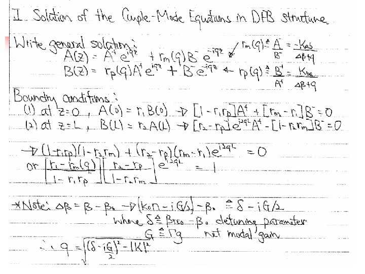
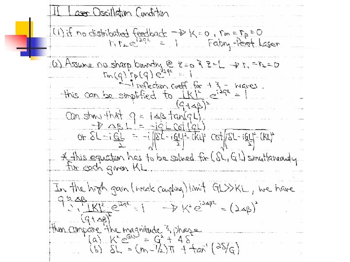
Solving for DFB Lasers
![Oscillation Condition Reflection gain contour in the L - L plane [2]](http://slidetodoc.com/presentation_image/322d000f2bfb840c7b5664dd9f036b8d/image-15.jpg "Oscillation Condition Reflection gain contour in the L - L plane [2]")
Oscillation Condition Reflection gain contour in the L - L plane [2]
![Regular DFB Laser [2]](http://slidetodoc.com/presentation_image/322d000f2bfb840c7b5664dd9f036b8d/image-16.jpg "Regular DFB Laser [2]")
Regular DFB Laser [2]
![/4 -Shifted DFB Laser [2]](http://slidetodoc.com/presentation_image/322d000f2bfb840c7b5664dd9f036b8d/image-17.jpg "/4 -Shifted DFB Laser [2]")
/4 -Shifted DFB Laser [2]

Gain-Coupled DFB Laser n n Complex : plug-in coupled mode equations with:
![Index- x Gain(Loss)-Coupled DFBs [2] n Index-coupled DFB lasers n n n have two](http://slidetodoc.com/presentation_image/322d000f2bfb840c7b5664dd9f036b8d/image-19.jpg "Index- x Gain(Loss)-Coupled DFBs [2] n Index-coupled DFB lasers n n n have two")
Index- x Gain(Loss)-Coupled DFBs [2] n Index-coupled DFB lasers n n n have two degenerate (longitudinal) modes Mode selection is based on facet phase very tricky and unreproducible Gain- or loss- coupled DFB n n Single wavelength More difficult to fabricate
 n n n Grating dimension ~ /4 n ~")
Fabrication (grating structure in DFB) n n n Grating dimension ~ /4 n ~ 100 nm (for ~1. 55 mm) Electron-beam lithography (EUV, X-ray, ion-beam, …) Interference of two UV lights. UV sensitive PR
 To create reflection mirrors on two sides of the cavity. Substrate is")
Dicing (edge-emitting-lasers) To create reflection mirrors on two sides of the cavity. Substrate is thinned down (~100 mm) before cleaving. After cleaving, protective coating is deposited on both facets to improve lifetime (mainly degraded by COD).

Notes on Fabrication n n n Smoothness of the gratings depends strongly on crystal orientation. Holographic photolithography or e-beam lithography are used to define the grating mask. Wet etch is used to etch the gratings. Dry etch may cause defects on the structure that propagate during the overgrowth. V-groove preferable to rectangular (grating quality). Growth rate depends strongly on the crystallographic orientation. Orientation of the growth depends on temperature. Epitaxial overgrowth is more complicated on the Ga. As material system than in In. P (oxidation).
![Grating Alignment [8] n n For growing into direction, grating must be aligned along](http://slidetodoc.com/presentation_image/322d000f2bfb840c7b5664dd9f036b8d/image-23.jpg "Grating Alignment [8] n n For growing into direction, grating must be aligned along")
Grating Alignment [8] n n For growing into direction, grating must be aligned along the direction. Generally, the dominant growth inside a v-groove is along the [111] plane.
![Surface Mass Transport (SMT) [8] n n Generation of [100] facets at the bottom](http://slidetodoc.com/presentation_image/322d000f2bfb840c7b5664dd9f036b8d/image-24.jpg "Surface Mass Transport (SMT) [8] n n Generation of [100] facets at the bottom")
Surface Mass Transport (SMT) [8] n n Generation of [100] facets at the bottom of the grooves due to diffusion of surface atoms. This process may eliminate the [111] facet.
![Wet-etched grating [8] n Wavy grating lines, nonflat side-walls and linkages between grooves can](http://slidetodoc.com/presentation_image/322d000f2bfb840c7b5664dd9f036b8d/image-25.jpg "Wet-etched grating [8] n Wavy grating lines, nonflat side-walls and linkages between grooves can")
Wet-etched grating [8] n Wavy grating lines, nonflat side-walls and linkages between grooves can be caused by undefined mask boarder or misalignment with respect to the crystal orientation.

Commercial DFB n Symbo l Min Typ Max Unit Components Parameters CW Output power(25 C) Pf 10 --- 30 m. W Threshold current It h -- 25 60 m. A Operating current If -- 300 -- m. A n Forward voltage Vf -- 2. 0 3. 0 V n Center Wavelength λc 1540 1550 1570 nm Linewidth Δ λ -- 2 -- MHz Monitor Current Im -- 200 -- μA Monitor dark current(Vr=5 V) Id -- -- 100 n. A Isolation(Optional) Iso -30 -- -- d. B TEC current ITEC -- 1. 2 -- A TEC voltage VTEC -- 3. 2 -- V Thermistor resistance(at 25℃) Rt h 9. 5 10 10. 5 kΩ Operating Temperature Range To -20 -- 65 C Storage temperature Tst g -40 -- 85 C n n DFB diode Thermoelectric cooler Thermistor Photodiode Optical isolator Fiber-coupled lens

Conclusion n n Overview of basic laser and DFB principles. Fabrication process depends on the growing method. Most critical step: grating. Transmitter used in most (all) long-haul WDM/DWDM systems. Tunable DFBs Forrest
![References [1] Verdeyen, J. T. - Laser Electronics, 3 rd Ed. , Prentice Hall,](http://slidetodoc.com/presentation_image/322d000f2bfb840c7b5664dd9f036b8d/image-28.jpg "References [1] Verdeyen, J. T. - Laser Electronics, 3 rd Ed. , Prentice Hall,")
References [1] Verdeyen, J. T. - Laser Electronics, 3 rd Ed. , Prentice Hall, USA, 1995. [2] Yariv, A. - Optical Electronics in Modern Communications, 5 th Ed. , Oxford Un. Press, New York, 1997. [3] Ghafouri-Shiraz, H. and Lo, B. S. K. - Distributed Feedback Lasers- Principles and Physical Modeling, John Wiley & Sons, England, 1996. [4] Carrol, J. , et. al. - Distributed Feedback Semiconductor Lasers, IEE, London, 1998. [5] Kinoshita, J. I. and Matsumoto, K. - “Transient chirping in distributed-feedback (DFB) lasers effect of spatial hole-burning along the laser axis”, IEEE J. Quantum Elec. , Vol. 24, n. 11, pp. 2160 -69, November 1988. [6] Coldren. L. A. and Corzine, - Diode Lasers and Photonics Integrated Circuits, John Wiley & Sons, New York, 1995. [7] Kamioka, H. , et. al. - “Reliability of an electro-absorption modulator integrated with a distributed feedback laser”, CLEO Pacific Rim 99: Procceedings, pp. 12023. [8] Chu, S. N. G. , et. al. - “Grating overgrowth and defect structures in distributedfeedback buried heterostructure laser diodes”, IEEE J. Sel. Top. in Quantum Elec. , Vol. 3, n. 3, pp. 862 -873, June 1997.
![References [9] Aoki, M. , et al. - “Novel structure MQW electroabsorption modulator/dfb-laser integrated](http://slidetodoc.com/presentation_image/322d000f2bfb840c7b5664dd9f036b8d/image-29.jpg "References [9] Aoki, M. , et al. - “Novel structure MQW electroabsorption modulator/dfb-laser integrated")
References [9] Aoki, M. , et al. - “Novel structure MQW electroabsorption modulator/dfb-laser integrated device fabricated by selective area MOCVD growth”, Elec. Lett. , Vol. 27, n. 23, pp. 2138 -40, November 1991. [10] Takigushi, T. , et al. - “Selective area MOCVD growth for novel 1. 3 m DFB laser diodes with graded grating”, 10 th Int. Conf. On In. P and Related Materials: Proceedings, Tsukuba, Japan, May 1998. [11] Osowski, M. L. , et al. - “An assymetric cladding gain-coupled DFB laser with oxide defined metal surface grating by MOCVD”, IEEE Phot. Tech. Lett. , Vol. 9, n. 11, pp. 1460 -62 , November 1997. [12] Luo, Y. et al. - “Fabrication and characteristics of gain-coupled DFB lasers with a corrugated active layer”, IEEE J. Quantum Elec. , Vol. 27, n. 6, pp. 1724 -31, June 1991. [13] Koontz, E. M. , et al. - “Overgrowth of submicron-patterned surfaces for buried index contrast devices”, J. of Semicond. Sci. Tech. , 15, R 1 -12, 2000. [14] Iga, K. and Kinoshita, S. - Process technology for semiconductor lasers, Springer Series in Materials Science, New York, 1996.
- Slides: 29