Discussion today Grating couplers Today we will design

- Slides: 33

Discussion today: Grating couplers • Today we will design and simulate a silicon photonic grating coupler using Lumerical FDTD 1

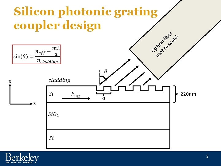
Silicon photonic grating coupler design er ) b fi ale l ica o sc t Op ot t (n 220 nm 2

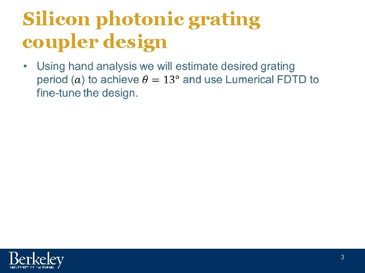
Silicon photonic grating coupler design • 3

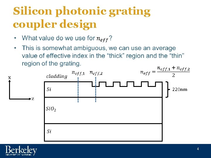
Silicon photonic grating coupler design • 220 nm 4

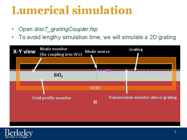
Lumerical simulation • Open disc 7_grating. Coupler. fsp • To avoid lengthy simulation time, we will simulate a 2 D grating X-Y view Mode monitor Mode source (for coupling into WG) Grating Si. O 2 FDTD Field profile monitor Si Transmission monitor above grating 5

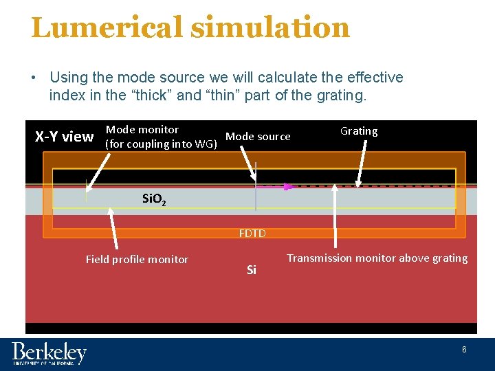
Lumerical simulation • Using the mode source we will calculate the effective index in the “thick” and “thin” part of the grating. X-Y view Mode monitor Mode source (for coupling into WG) Grating Si. O 2 FDTD Field profile monitor Si Transmission monitor above grating 6

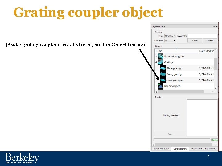
Grating coupler object (Aside: grating coupler is created using built-in Object Library) 7

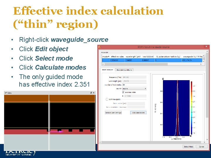
Effective index calculation (“thin” region) • • • Right-click waveguide_source Click Edit object Click Select mode Click Calculate modes The only guided mode has effective index 2. 351 8

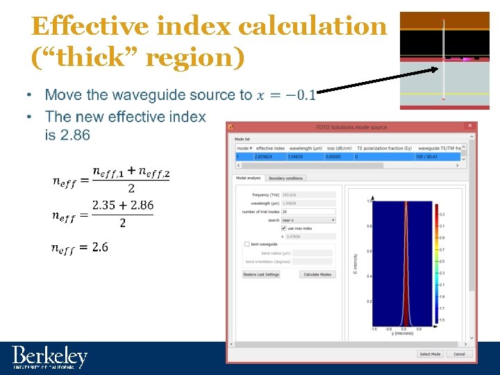
Effective index calculation (“thick” region) • 9

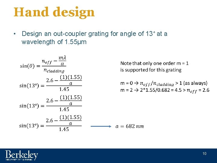
Hand design • Design an out-coupler grating for angle of 13° at a wavelength of 1. 55µm 10

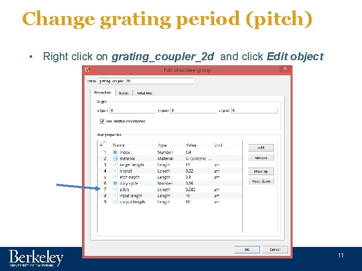
Change grating period (pitch) • Right click on grating_coupler_2 d and click Edit object 11

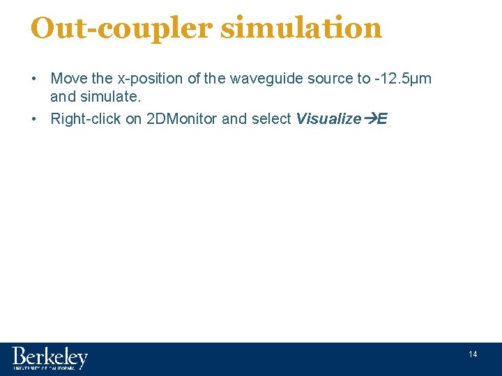
Out-coupler simulation • Move the x-position of the waveguide source to -12. 5µm and simulate. • Right-click on 2 DMonitor and select Visualize E 14

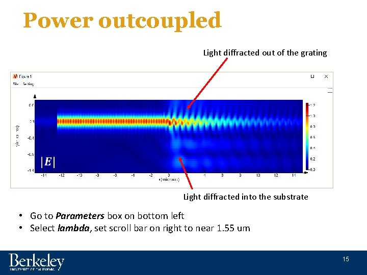
Power outcoupled Light diffracted out of the grating Light diffracted into the substrate • Go to Parameters box on bottom left • Select lambda, set scroll bar on right to near 1. 55 um 15

Power outcoupled • Right-click on above. Monitor and select Visualize T 16

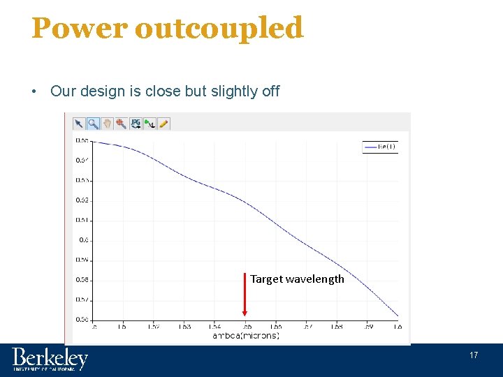
Power outcoupled • Our design is close but slightly off Target wavelength 17

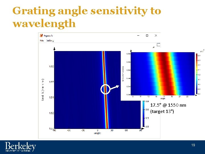
Grating angle sensitivity to wavelength • Right-click on above. Monitor and select Visualize Farfield all 18

Grating angle sensitivity to wavelength 17. 5° @ 1550 nm (target 13°) 19

In-coupler grating design • Let’s see how well our grating coupler works for coupling light into a waveguide. • Go back to Layout mode • Right-click waveguide_source→Disable • Right-click source→Enable. This is a Gaussian source we will use first to approximate the fiber. 20

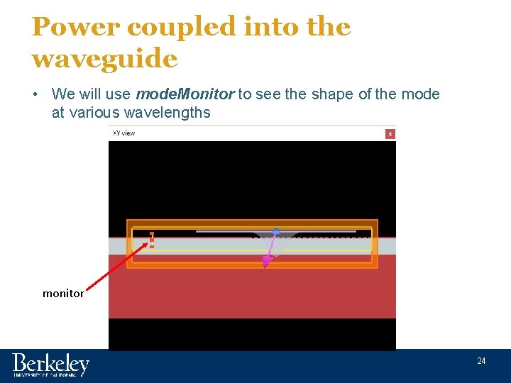
Power coupled into the waveguide • We will use mode. Monitor to see the shape of the mode at various wavelengths monitor 24

In-coupler grating simulation • Simulate • Right-click on 2 DMonitor and select Visualize E 26

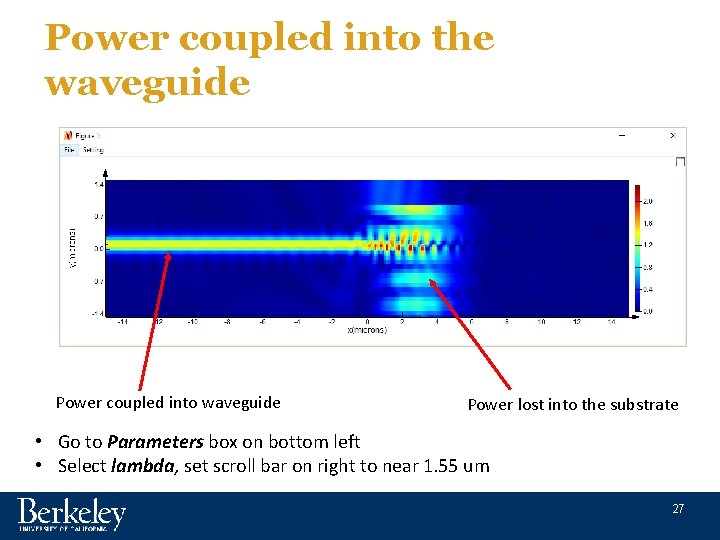
Power coupled into the waveguide Power coupled into waveguide Power lost into the substrate • Go to Parameters box on bottom left • Select lambda, set scroll bar on right to near 1. 55 um 27

Mode monitor • Right-click on mode. Monitor and select Visualize T 28

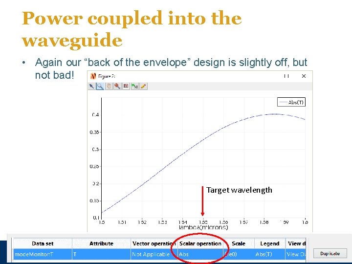
Power coupled into the waveguide • Again our “back of the envelope” design is slightly off, but not bad! Target wavelength 29

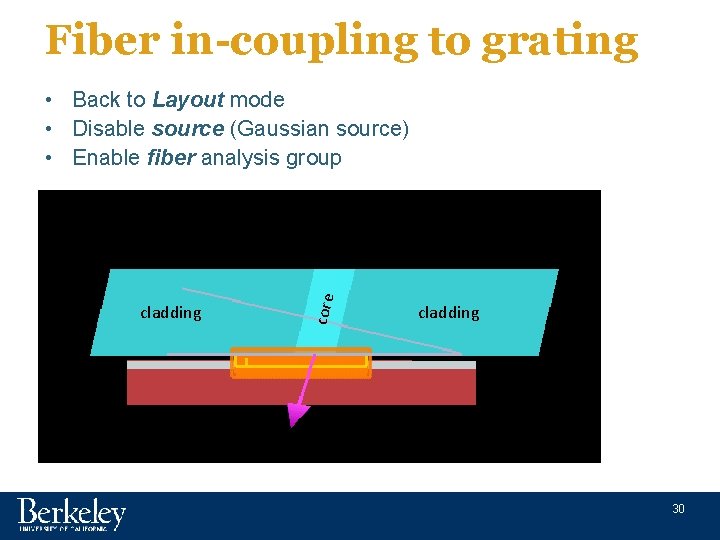
Fiber in-coupling to grating cladding core • Back to Layout mode • Disable source (Gaussian source) • Enable fiber analysis group cladding 30

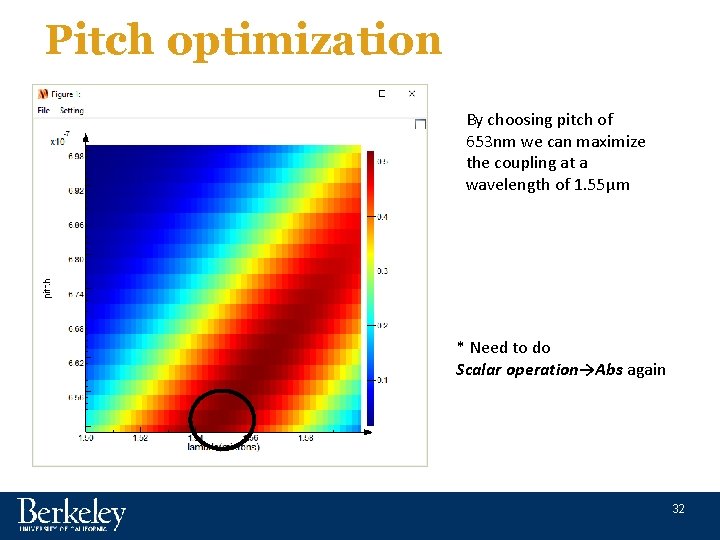
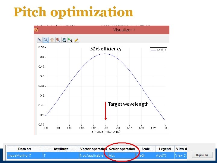
Pitch optimization • Using more realistic fiber geometry let’s optimize the grating pitch so that the coupling peaks at 1. 55µm. • A sweep plan has already been generated called pitch. Sweep. This will sweep the pitch from 650 nm to 700 nm. • Run pitch. Sweep at home (this will run 20 simulations, ~3 -4 min) • Right-click pitch. Sweep and select Visualize Mode. T 31

Pitch optimization By choosing pitch of 653 nm we can maximize the coupling at a wavelength of 1. 55µm * Need to do Scalar operation→Abs again 32

Pitch optimization • Change grating_coupler_2 D pitch to 653 nm • Run simulation • Right-click on 2 DMonitor and select Visualize E 33

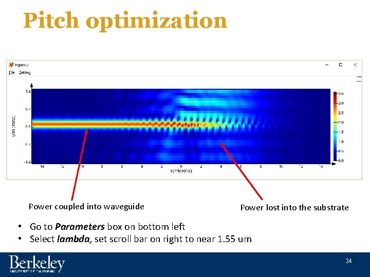
Pitch optimization Power coupled into waveguide Power lost into the substrate • Go to Parameters box on bottom left • Select lambda, set scroll bar on right to near 1. 55 um 34

Mode monitor • Right-click on mode. Monitor and select Visualize T 35

Pitch optimization 52% efficiency Target wavelength 36

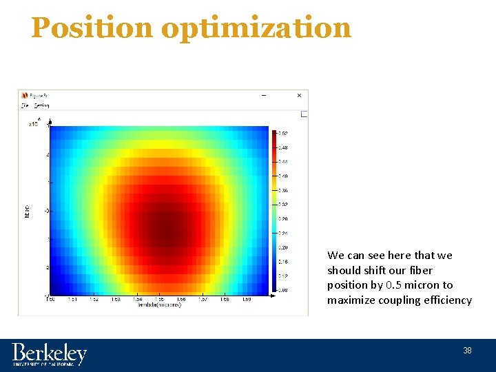
Position optimization • Coupling efficiency will be dependent upon the position of the fiber with respect to the grating • A sweep plan has been generated to sweep the fiber +/- 3 microns in the x-direction. – Note: It’s actually easier here to move the x-position of the grating but this accomplishes the same thing • Run x. Sweep at home (this will run 20 simulations) • Right-click x. Sweep and select Visualize Mode. T 37

Position optimization We can see here that we should shift our fiber position by 0. 5 micron to maximize coupling efficiency 38

Next discussion • Next discussion we will close the grating coupler topic by showing how to extract the grating S-parameters and how to import into the photonic circuit solver Lumerical Interconnect. • This will be particularly useful for the final project if you wish to simulate large structures. 39