DIRECT MEMORY ACCESS MODULE DMA M Direct Memory

- Slides: 28

DIRECT MEMORY ACCESS MODULE (DMA) M Direct Memory Access Module MTT 48 10 - 1


Module Objective By the end of this module, you should be able to: • Configure the DMA • Service TIM, SPI and SCI interrupts via DMA • Initiate DMA block data transfers Module Exercise: M • Service TIM channel output compare via DMA • Service SPI transmission complete via DMA • Service SCI received data via DMA • Initiate block data moves Direct Memory Access Module MTT 48 10 - 3

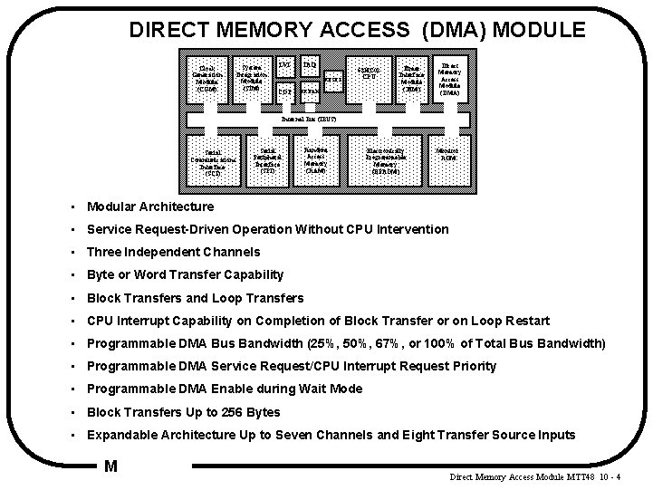
DIRECT MEMORY ACCESS (DMA) MODULE Clock Generation Module (CGM) System Integration Module (SIM) LVI IRQ COP BREAK RESET 68 HC 08 CPU Timer Interface Module (TIM) Direct Memory Access Module (DMA) Internal Bus (IBUS) Serial Communications Interface (SCI) Serial Peripheral Interface (SPI) Random Access Memory (RAM) Electronically Programmable Memory (EPROM) Monitor ROM • Modular Architecture • Service Request-Driven Operation Without CPU Intervention • Three Independent Channels • Byte or Word Transfer Capability • Block Transfers and Loop Transfers • CPU Interrupt Capability on Completion of Block Transfer or on Loop Restart • Programmable DMA Bus Bandwidth (25%, 50%, 67%, or 100% of Total Bus Bandwidth) • Programmable DMA Service Request/CPU Interrupt Request Priority • Programmable DMA Enable during Wait Mode • Block Transfers Up to 256 Bytes • Expandable Architecture Up to Seven Channels and Eight Transfer Source Inputs M Direct Memory Access Module MTT 48 10 - 4

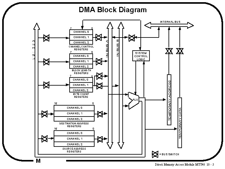
DMA Block Diagram INTERNAL BUS 7 0 CHANNEL 1 CHANNEL 2 CHANNEL CONTROL REGISTERS 7 0 SYSTEM CONTROL LOGIC CHANNEL 0 CHANNEL 1 CHANNEL 2 7 BLOCK LENGTH REGISTERS 0 CHANNEL 1 • CHANNEL 2 BYTE COUNT REGISTERS 15 ALU 0 CHANNEL 1 CHANNEL 2 15 DESTINATION ADDRESS REGISTERS 0 CHANNEL 1 CHANNEL 2 SOURCE ADDRESS REGISTERS M = BUS SWITCH Direct Memory Access Module MTT 48 10 - 5

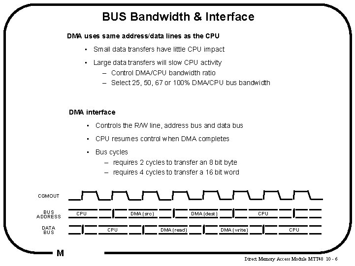
BUS Bandwidth & Interface DMA uses same address/data lines as the CPU • Small data transfers have little CPU impact • Large data transfers will slow CPU activity – Control DMA/CPU bandwidth ratio – Select 25, 50, 67 or 100% DMA/CPU bus bandwidth DMA interface • Controls the R/W line, address bus and data bus • CPU resumes control when DMA completes • Bus cycles – requires 2 cycles to transfer an 8 bit byte – requires 4 cycles to transfer a 16 bit word CGMOUT BUS ADDRESS DATA BUS CPU DMA (src) CPU M DMA (dest) DMA (read) CPU DMA (write) CPU Direct Memory Access Module MTT 48 10 - 6

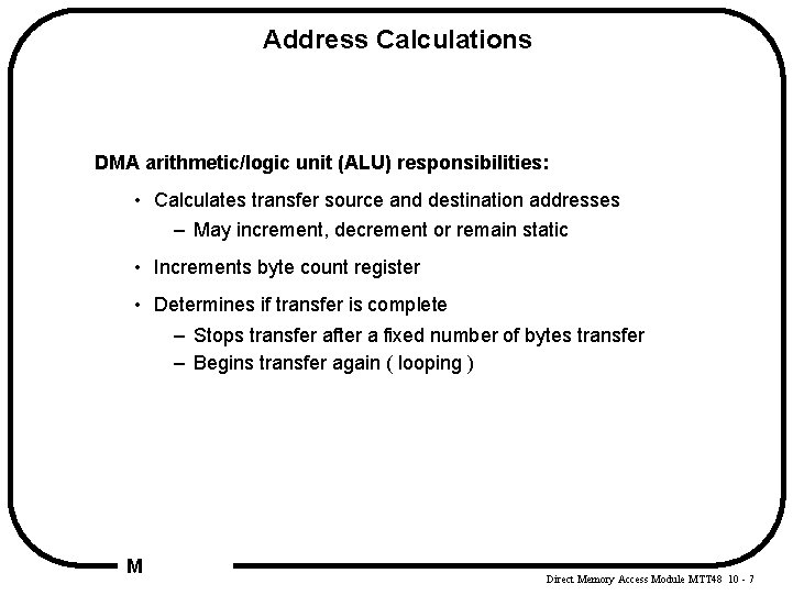
Address Calculations DMA arithmetic/logic unit (ALU) responsibilities: • Calculates transfer source and destination addresses – May increment, decrement or remain static • Increments byte count register • Determines if transfer is complete – Stops transfer after a fixed number of bytes transfer – Begins transfer again ( looping ) M Direct Memory Access Module MTT 48 10 - 7

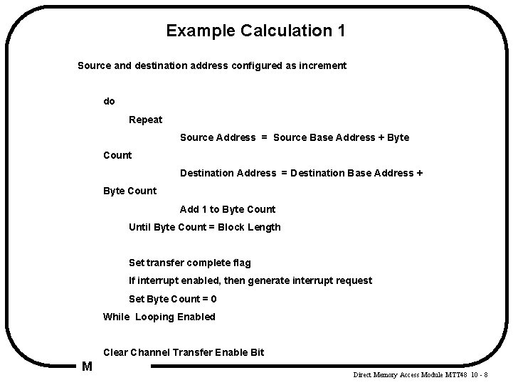
Example Calculation 1 Source and destination address configured as increment do Repeat Source Address = Source Base Address + Byte Count Destination Address = Destination Base Address + Byte Count Add 1 to Byte Count Until Byte Count = Block Length Set transfer complete flag If interrupt enabled, then generate interrupt request Set Byte Count = 0 While Looping Enabled Clear Channel Transfer Enable Bit M Direct Memory Access Module MTT 48 10 - 8

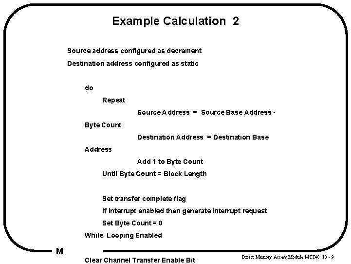
Example Calculation 2 Source address configured as decrement Destination address configured as static do Repeat Source Address = Source Base Address Byte Count Destination Address = Destination Base Address Add 1 to Byte Count Until Byte Count = Block Length Set transfer complete flag If interrupt enabled then generate interrupt request Set Byte Count = 0 While Looping Enabled M Clear Channel Transfer Enable Bit Direct Memory Access Module MTT 48 10 - 9

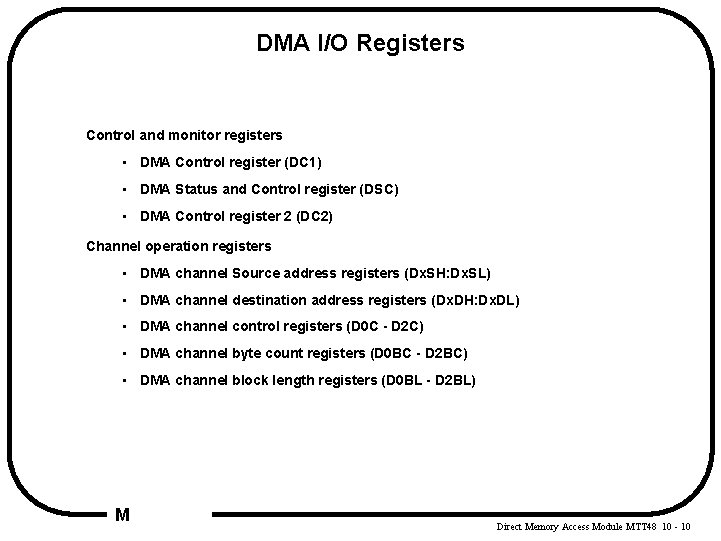
DMA I/O Registers Control and monitor registers • DMA Control register (DC 1) • DMA Status and Control register (DSC) • DMA Control register 2 (DC 2) Channel operation registers • DMA channel Source address registers (Dx. SH: Dx. SL) • DMA channel destination address registers (Dx. DH: Dx. DL) • DMA channel control registers (D 0 C - D 2 C) • DMA channel byte count registers (D 0 BC - D 2 BC) • DMA channel block length registers (D 0 BL - D 2 BL) M Direct Memory Access Module MTT 48 10 - 10

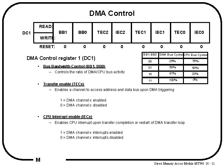
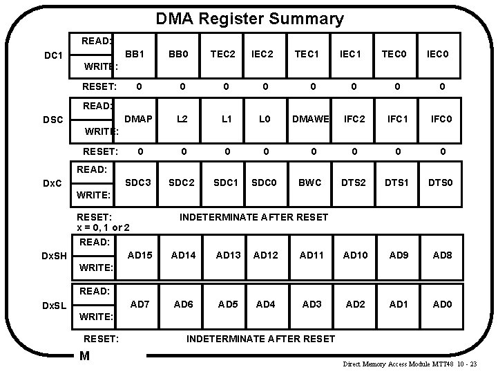
DMA Control READ: DC 1 BB 0 0 0 TEC 2 IEC 2 TEC 1 IEC 1 TEC 0 IEC 0 WRITE: RESET: 0 0 DMA Control register 1 (DC 1) • Bus Bandwidth Control (BB 1, BB 0) – Controls the ratio of DMA/CPU bus activity • Transfer enable (TECx) 0 0 BB 1: BB 0 DMA Bus Cycles. CPU Bus Cycles 00 25% 75% 01 50% 10 67% 33% 11 100% 0% – Enables a channel to access address and data bus upon DMA triggering 1 = DMA channel x enabled 0 = DMA channel x disabled • CPU Interrupt enable (IECx) – Enables CPU interrupt upon transfer completion or restart of DMA transfer loop 1 = DMA channel x interrupts enabled 0 = DMA channel x interrupts disabled M Direct Memory Access Module MTT 48 10 - 11

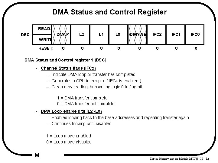
DMA Status and Control Register READ: DSC DMAP L 2 L 1 L 0 0 0 DMAWE IFC 2 IFC 1 IFC 0 0 WRITE: RESET: 0 DMA Status and Control register 1 (DSC) • Channel Status flags (IFCx) – Indicate DMA loop or transfer has completed – Generates a CPU interrupt ( if IECx is enabled ) – Cleared by reading then writing logic 0 to flag bit 1 = DMA transfer complete 0 = DMA transfer not complete • DMA Loop enable bits (L 2 -L 0) – Enables looping back to the base addresses and repeating transfer again – Continues looping until disabled 1 = Loop mode enabled 0 = Loop mode disabled M Direct Memory Access Module MTT 48 10 - 12

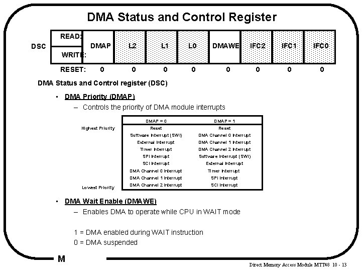
DMA Status and Control Register READ: DSC DMAP L 2 L 1 L 0 0 0 DMAWE IFC 2 IFC 1 IFC 0 0 WRITE: RESET: 0 DMA Status and Control register (DSC) • DMA Priority (DMAP) – Controls the priority of DMA module interrupts Highest Priority Lowest Priority DMAP = 0 DMAP = 1 Reset Software Interrupt (SWI) DMA Channel 0 Interrupt External Interrupt DMA Channel 1 Interrupt Timer Interrupt DMA Channel 2 Interrupt SPI Interrupt Software Interrupt (SWI) SCI Interrupt External Interrupt DMA Channel 0 Interrupt Timer Interrupt DMA Channel 1 Interrupt SPI Interrupt DMA Channel 2 Interrupt SCI Interrupt • DMA Wait Enable (DMAWE) – Enables DMA to operate while CPU in WAIT mode 1 = DMA enabled during WAIT instruction 0 = DMA suspended M Direct Memory Access Module MTT 48 10 - 13

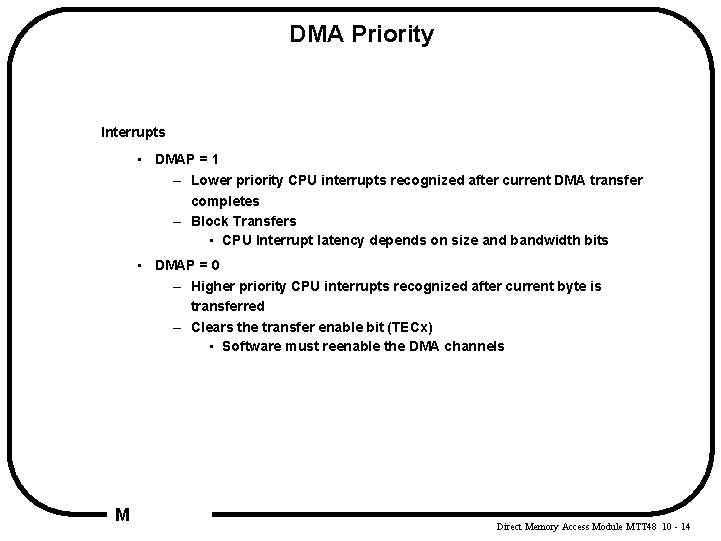
DMA Priority Interrupts • DMAP = 1 – Lower priority CPU interrupts recognized after current DMA transfer completes – Block Transfers • CPU Interrupt latency depends on size and bandwidth bits • DMAP = 0 – Higher priority CPU interrupts recognized after current byte is transferred – Clears the transfer enable bit (TECx) • Software must reenable the DMA channels M Direct Memory Access Module MTT 48 10 - 14

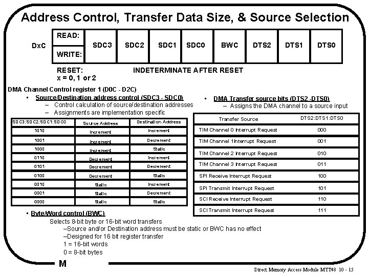
Address Control, Transfer Data Size, & Source Selection READ: SDC 3 Dx. C SDC 2 SDC 1 SDC 0 BWC DTS 2 DTS 1 DTS 0 WRITE: RESET: x = 0, 1 or 2 INDETERMINATE AFTER RESET DMA Channel Control register 1 (D 0 C - D 2 C) • Source/Destination address control (SDC 3 - SDC 0) – Control calculation of source/destination addresses – Assignments are implementation specific • DMA Transfer source bits (DTS 2 -DTS 0) – Assigns the DMA channel to a source input Transfer Source DTS 2: DTS 1: DTS 0 Increment TIM Channel 0 Interrupt Request 000 Increment Decrement TIM Channel 1 Interrupt Request 001 1000 Increment Static 0110 Increment TIM Channel 2 Interrupt Request 010 Decrement 0101 Decrement TIM Channel 3 Interrupt Request 011 0100 Decrement Static SPI Receive Interrupt Request 100 0010 Static Increment 0001 Static Decrement SPI Transmit Interrupt Request 101 0000 Static SCI Receive Interrupt Request 110 SCI Transmit Interrupt Request 111 SDC 3: SDC 2: SDC 1: SDC 0 Source Address Destination Address 1010 Increment 1001 • Byte/Word control (BWC) Selects 8 -bit byte or 16 -bit word transfers –Source and/or Destination address must be static or BWC has no effect –Designed for 16 bit register transfer 1 = 16 -bit words 0 = 8 -bit bytes M Direct Memory Access Module MTT 48 10 - 15

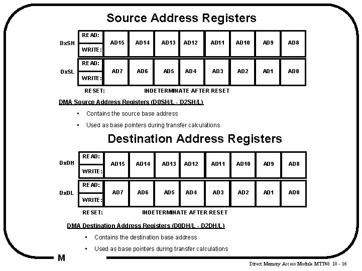
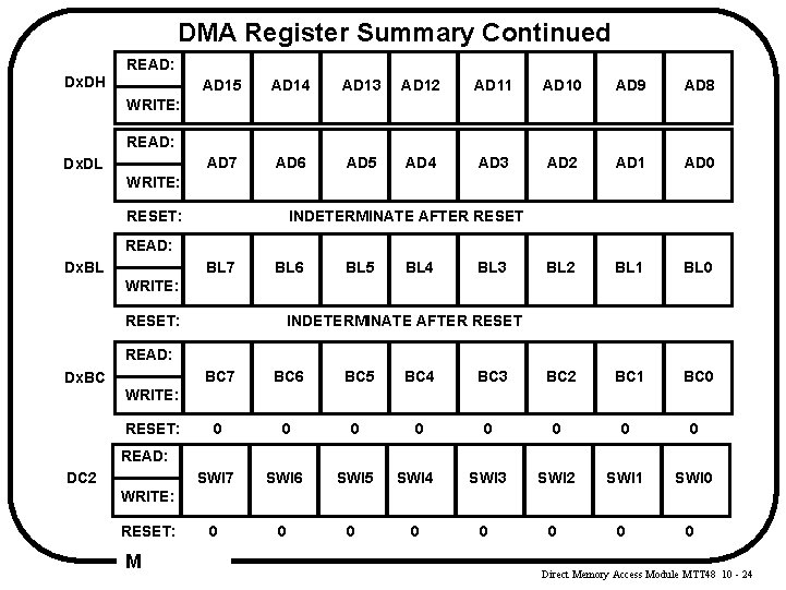
Source Address Registers READ: Dx. SH AD 15 AD 14 AD 13 AD 12 AD 11 AD 10 AD 9 AD 8 AD 7 AD 6 AD 5 AD 4 AD 3 AD 2 AD 1 AD 0 WRITE: READ: Dx. SL WRITE: RESET: INDETERMINATE AFTER RESET DMA Source Address Registers (D 0 SH/L - D 2 SH/L) • Contains the source base address • Used as base pointers during transfer calculations Destination Address Registers READ: Dx. DH AD 15 AD 14 AD 13 AD 12 AD 11 AD 10 AD 9 AD 8 AD 7 AD 6 AD 5 AD 4 AD 3 AD 2 AD 1 AD 0 WRITE: READ: Dx. DL WRITE: RESET: INDETERMINATE AFTER RESET DMA Destination Address Registers (D 0 DH/L - D 2 DH/L) M • Contains the destination base address • Used as base pointers during transfer calculations Direct Memory Access Module MTT 48 10 - 16

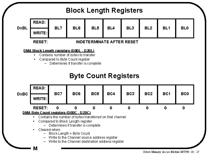
Block Length Registers READ: Dx. BL BL 7 BL 6 BL 5 BL 4 BL 3 BL 2 BL 1 BL 0 WRITE: RESET: INDETERMINATE AFTER RESET DMA Block Length registers (D 0 BL - D 2 BL) • Contains number of bytes to transfer • Compared to Byte Count register – Determines if transfer is complete Byte Count Registers READ: Dx. BC BC 7 BC 6 BC 5 BC 4 BC 3 BC 2 BC 1 BC 0 0 0 0 0 WRITE: RESET: DMA Byte Count registers (D 0 BC - D 2 BC) • Contains the number of bytes transferred on that channel • Compared to Block Length register – Determines if transfer is complete • Cleared when: – Block Length = Byte Count – Write to the Channel source address register – Write to the Channel destination address register M Direct Memory Access Module MTT 48 10 - 17

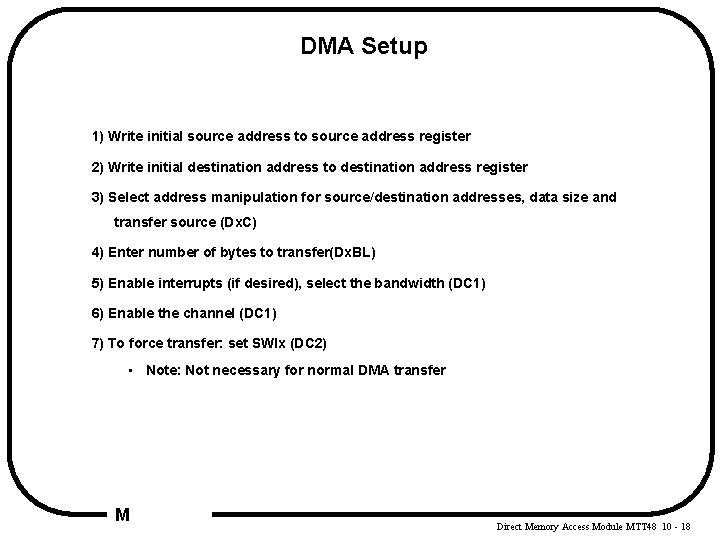
DMA Setup 1) Write initial source address to source address register 2) Write initial destination address to destination address register 3) Select address manipulation for source/destination addresses, data size and transfer source (Dx. C) 4) Enter number of bytes to transfer(Dx. BL) 5) Enable interrupts (if desired), select the bandwidth (DC 1) 6) Enable the channel (DC 1) 7) To force transfer: set SWIx (DC 2) • Note: Not necessary for normal DMA transfer M Direct Memory Access Module MTT 48 10 - 18

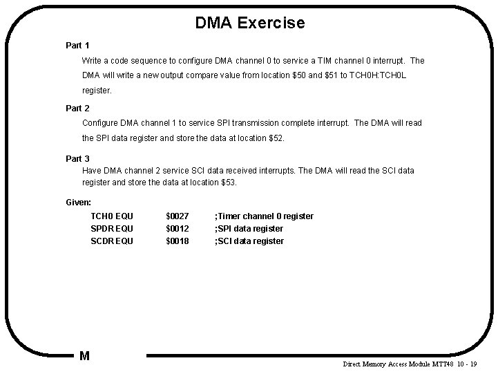
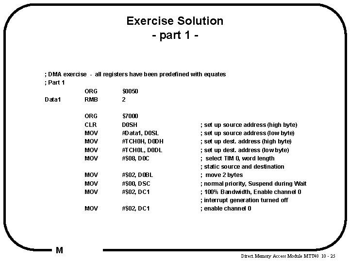
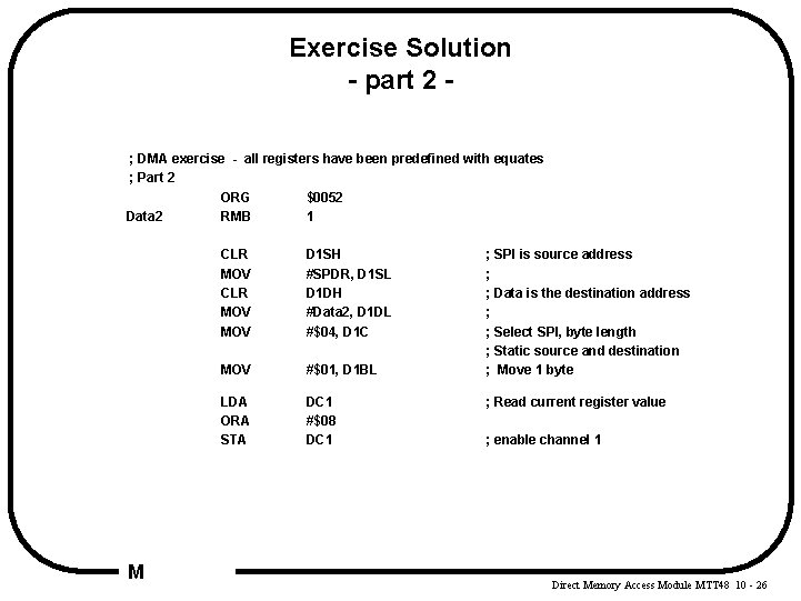
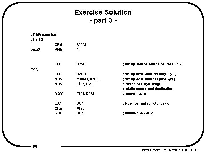
DMA Exercise Part 1 Write a code sequence to configure DMA channel 0 to service a TIM channel 0 interrupt. The DMA will write a new output compare value from location $50 and $51 to TCH 0 H: TCH 0 L register. Part 2 Configure DMA channel 1 to service SPI transmission complete interrupt. The DMA will read the SPI data register and store the data at location $52. Part 3 Have DMA channel 2 service SCI data received interrupts. The DMA will read the SCI data register and store the data at location $53. Given: TCH 0 EQU SPDR EQU SCDR EQU M $0027 $0012 $0018 ; Timer channel 0 register ; SPI data register ; SCI data register Direct Memory Access Module MTT 48 10 - 19

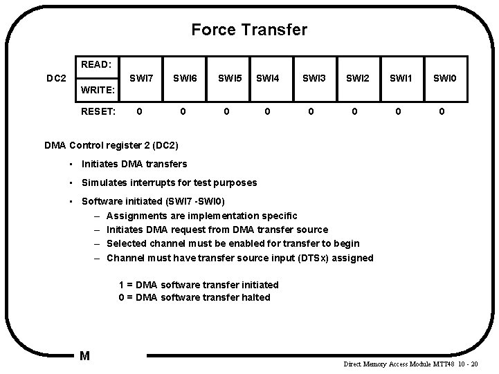
Force Transfer READ: DC 2 SWI 7 SWI 6 SWI 5 SWI 4 SWI 3 SWI 2 SWI 1 SWI 0 0 0 0 0 WRITE: RESET: DMA Control register 2 (DC 2) • Initiates DMA transfers • Simulates interrupts for test purposes • Software initiated (SWI 7 -SWI 0) – Assignments are implementation specific – Initiates DMA request from DMA transfer source – Selected channel must be enabled for transfer to begin – Channel must have transfer source input (DTSx) assigned 1 = DMA software transfer initiated 0 = DMA software transfer halted M Direct Memory Access Module MTT 48 10 - 20

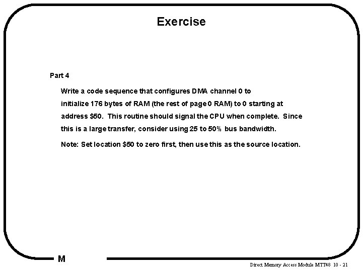
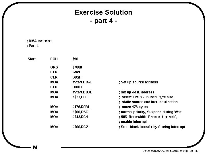
Exercise Part 4 Write a code sequence that configures DMA channel 0 to initialize 176 bytes of RAM (the rest of page 0 RAM) to 0 starting at address $50. This routine should signal the CPU when complete. Since this is a large transfer, consider using 25 to 50% bus bandwidth. Note: Set location $50 to zero first, then use this as the source location. M Direct Memory Access Module MTT 48 10 - 21

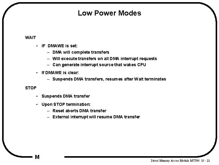
Low Power Modes WAIT • IF DMAWE is set: – DMA will complete transfers – Will execute transfers on all DMA interrupt requests – Can generate interrupt source that wakes CPU • If DMAWE is clear: – Suspends DMA transfers, resumes after Wait terminates STOP • Suspends DMA transfer • Upon STOP termination: – Reset aborts DMA transfer – External interrupt will resume DMA transfer M Direct Memory Access Module MTT 48 10 - 22

DMA Register Summary READ: DC 1 BB 0 TEC 2 IEC 2 TEC 1 IEC 1 TEC 0 IEC 0 0 0 0 0 DMAP L 2 L 1 L 0 DMAWE IFC 2 IFC 1 IFC 0 0 0 0 SDC 3 SDC 2 SDC 1 SDC 0 DTS 2 DTS 1 DTS 0 WRITE: RESET: READ: DSC WRITE: RESET: 0 READ: Dx. C BWC WRITE: RESET: x = 0, 1 or 2 INDETERMINATE AFTER RESET READ: Dx. SH AD 15 AD 14 AD 13 AD 12 AD 11 AD 10 AD 9 AD 8 AD 7 AD 6 AD 5 AD 4 AD 3 AD 2 AD 1 AD 0 WRITE: READ: Dx. SL WRITE: RESET: M INDETERMINATE AFTER RESET Direct Memory Access Module MTT 48 10 - 23

DMA Register Summary Continued READ: Dx. DH AD 15 AD 14 AD 13 AD 12 AD 11 AD 10 AD 9 AD 8 AD 7 AD 6 AD 5 AD 4 AD 3 AD 2 AD 1 AD 0 BL 2 BL 1 BL 0 WRITE: READ: Dx. DL WRITE: RESET: INDETERMINATE AFTER RESET READ: Dx. BL BL 7 BL 6 BL 5 BL 4 BL 3 WRITE: RESET: INDETERMINATE AFTER RESET READ: Dx. BC BC 7 BC 6 BC 5 BC 4 BC 3 BC 2 BC 1 BC 0 0 0 0 0 SWI 7 SWI 6 SWI 5 SWI 4 SWI 3 SWI 2 SWI 1 SWI 0 0 0 0 0 WRITE: RESET: READ: DC 2 WRITE: RESET: M Direct Memory Access Module MTT 48 10 - 24

Exercise Solution - part 1 - ; DMA exercise - all registers have been predefined with equates ; Part 1 ORG $0050 Data 1 RMB 2 M ORG CLR MOV MOV $7000 D 0 SH #Data 1, D 0 SL #TCH 0 H, D 0 DH #TCH 0 L, D 0 DL #$08, D 0 C MOV MOV #$02, D 0 BL #$00, DSC #$02, DC 1 MOV #$02, DC 1 ; set up source address (high byte) ; set up source address (low byte) ; set up dest. address (high byte) ; set up dest. address (low byte) ; select TIM 0, word length ; static source and destination ; move 2 bytes ; normal priority, Suspend during Wait ; 100% Bandwidth, Enable channel 0 ; interrupt generation turned off ; enable channel 0 Direct Memory Access Module MTT 48 10 - 25

Exercise Solution - part 2 ; DMA exercise - all registers have been predefined with equates ; Part 2 ORG $0052 Data 2 RMB 1 M CLR MOV MOV D 1 SH #SPDR, D 1 SL D 1 DH #Data 2, D 1 DL #$04, D 1 C MOV #$01, D 1 BL LDA ORA STA DC 1 #$08 DC 1 ; SPI is source address ; ; Data is the destination address ; ; Select SPI, byte length ; Static source and destination ; Move 1 byte ; Read current register value ; enable channel 1 Direct Memory Access Module MTT 48 10 - 26

Exercise Solution - part 3 ; DMA exercise ; Part 3 ORG Data 3 RMB $0053 1 CLR D 2 SH ; set up source address (low CLR MOV D 2 DH #Data 3, D 2 DL #$06, D 2 C MOV #$01, D 2 BL ; set up dest. address (high byte) ; set up dest. address (low byte) ; select SCI, byte length ; static source and destination ; move 1 byte LDA ORA STA DC 1 #$20 DC 1 byte) M ; Read current register value ; enable channel 2 Direct Memory Access Module MTT 48 10 - 27

Exercise Solution - part 4 ; DMA exercise ; Part 4 Start M EQU $50 ORG CLR MOV $7000 Start D 0 SH #Start, D 0 SL D 0 DH #Start, D 0 DL #$23, D 0 C MOV MOV #176, D 0 BL #$00, DSC #$43, DC 1 MOV #$08, DC 2 ; Set up source address ; set up dest. address ; select TIM 3 - unused, byte size ; static source and incr. destination ; move 176 bytes ; normal priority, Suspend during Wait ; 50% Bandwidth, Enable channel 0, ; enable interrupt ; Start block transfer by forcing interrupt Direct Memory Access Module MTT 48 10 - 28