Diode simulations and measurements Daniel Molnar Dipole diode






- Slides: 53

Diode simulations and measurements Daniel Molnar

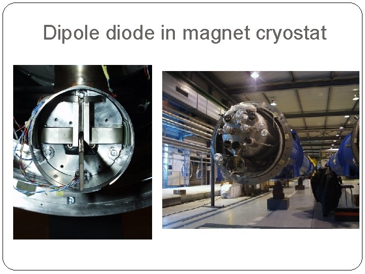
Dipole diode in magnet cryostat

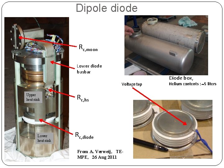
Dipole diode Rc, moon Lower diode busbar Diode box, Voltage tap Upper heat sink Lower heat sink Rc, hs Rc, diode From A. Verweij, TEMPE, 26 Aug 2011 Helium contents : 5 liters

Quadropole diode “Half-moons” Leads with 3(or 2) bolts Diodes(identical to dipole)

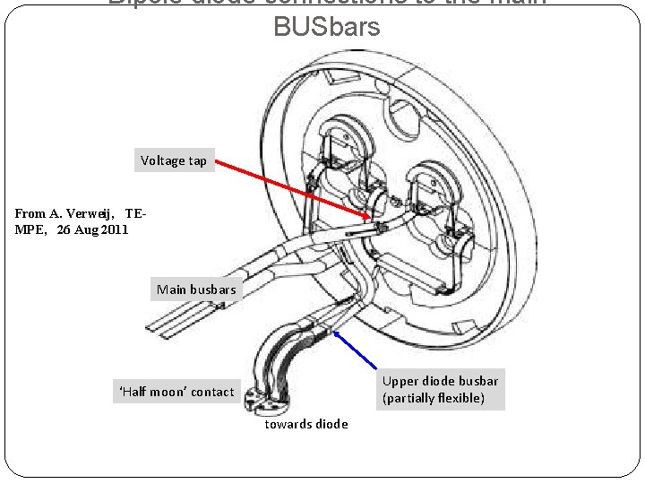
Dipole diode connections to the main BUSbars Voltage tap From A. Verweij, TEMPE, 26 Aug 2011 Main busbars Upper diode busbar (partially flexible) ‘Half moon’ contact towards diode

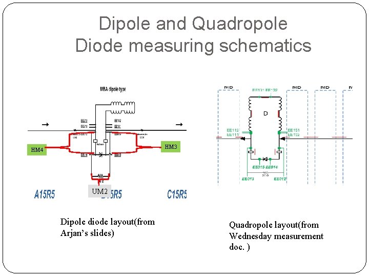
Dipole and Quadropole Diode measuring schematics HM 3 HM 4 UM 2 Dipole diode layout(from Arjan’s slides) Quadropole layout(from Wednesday measurement doc. )

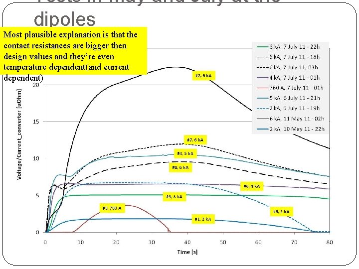
Tests in May and July at the dipoles Most plausible explanation is that the contact resistances are bigger then design values and they’re even temperature dependent(and current dependent)

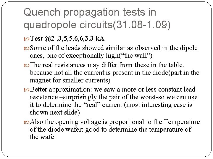
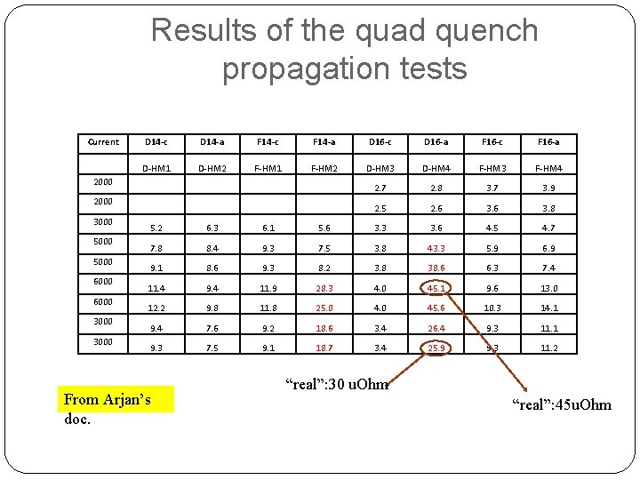
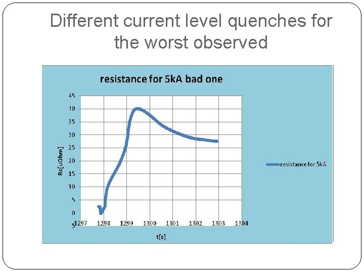
Quench propagation tests in quadropole circuits(31. 08 -1. 09) Test @2 , 3, 5, 5, 6, 6, 3, 3 k. A Some of the leads showed similar as observed in the dipole ones, one of exceptionally high(“the wall”) The real resistances may differ from these in the table, because not all the current is present in the diode(part in the magnet for smaller currents) Better approximation: we saw a more or less constant lead resistance –surprisingly the pair of the worst-so we can use it to determine the “real” current (most interesting case is shown next slide) Also the opening voltage is proportional to the Temperature of the diode wafer: good to determine the temperature of the wafer

Results of the quad quench propagation tests Current D 14 -c D 14 -a F 14 -c F 14 -a D 16 -c D 16 -a F 16 -c F 16 -a D-HM 1 D-HM 2 F-HM 1 F-HM 2 D-HM 3 D-HM 4 F-HM 3 F-HM 4 2. 7 2. 8 3. 7 3. 9 2. 5 2. 6 3. 8 2000 3000 5000 6000 3000 5. 2 6. 3 6. 1 5. 6 3. 3 3. 6 4. 5 4. 7 7. 8 8. 4 9. 3 7. 5 3. 8 43. 3 5. 9 6. 9 9. 1 8. 6 9. 3 8. 2 3. 8 38. 6 6. 3 7. 4 11. 4 9. 4 11. 9 28. 3 4. 0 45. 1 9. 6 13. 0 12. 2 9. 8 11. 8 25. 0 45. 6 10. 3 14. 1 9. 4 7. 6 9. 2 18. 6 3. 4 26. 4 9. 3 11. 1 9. 3 7. 5 9. 1 18. 7 3. 4 25. 9 9. 3 11. 2 From Arjan’s doc. “real”: 30 u. Ohm “real”: 45 u. Ohm

Different current level quenches for the worst observed

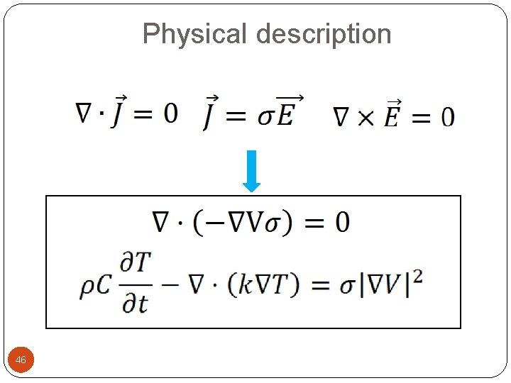
Modeling the diodes The models takes the Joule heating as the base physical description, but later other physics were added Reasonable simplifications i. e. : insignificant, tiny details are excluded, such as the actual shape of the heat sink Different contact resistance values have been investigated, to check how we can come up with the results shown above, and to check the maximum temperature But : a contact is a micro effect, we model macro, so we also need the micro model (according to literature!) of a contact The same stand for the Quadropole diodes

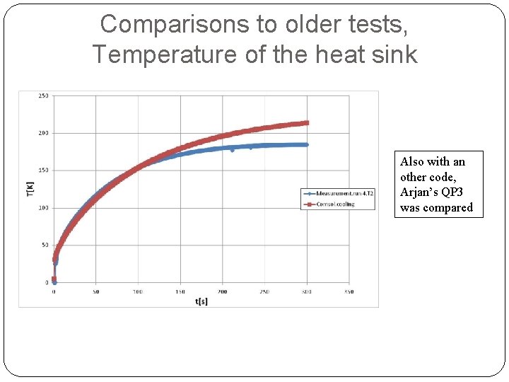
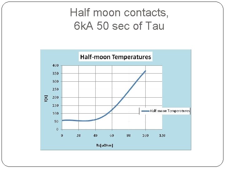
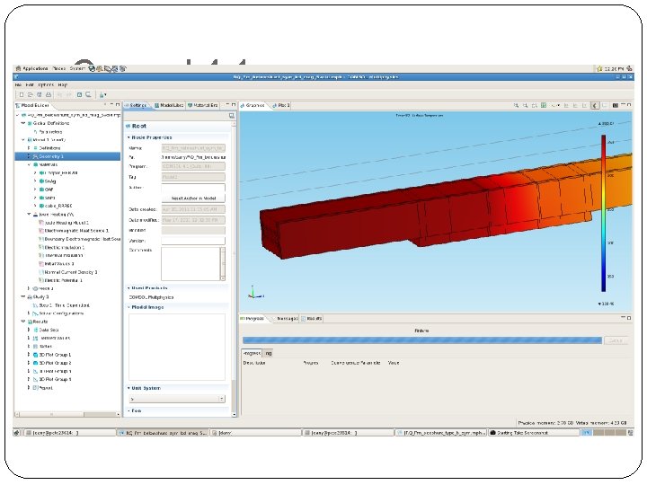
Modeling in Comsol Model of the diode itself is just a resistor, which is varying with the current, since the voltage is assumed as a constant(1 V) Adiabatic thermal boundary conditions, with initial temperature of 10 K(in some cases cooling to He as well ) Electrically is a current constraint problem, with the exponential decaying current; most cases for 6 k. A and 50 sec of Tau First the modeled Temperatures have been compared to previous measurements(in SM 18 or other place not in the machine!) First assumption 0 contact resistance everywhere: impossible but ideal world must be nice in other aspects of life too

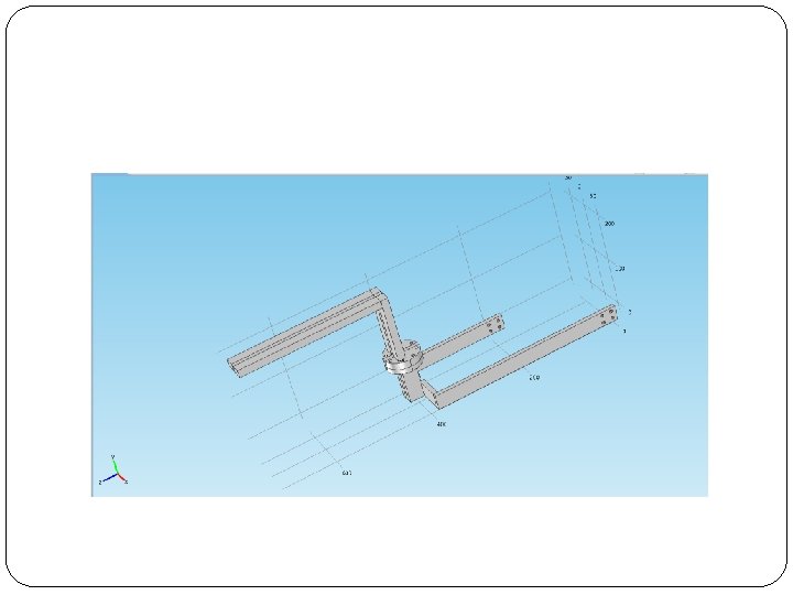
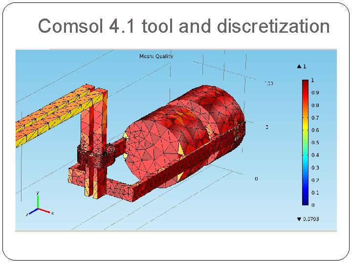
Comsol 4. 1 tool and discretization

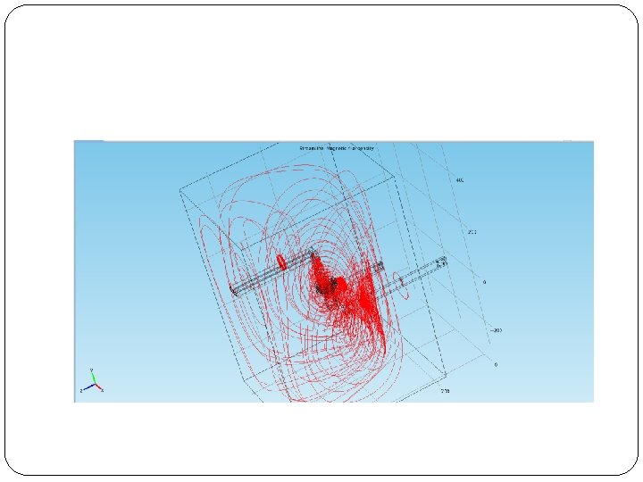
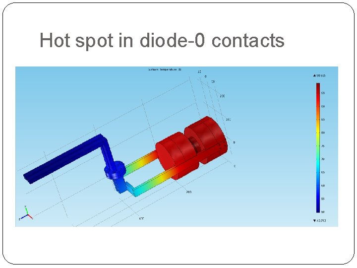
Hot spot in diode-0 contacts

Comparisons to older tests, Temperature of the heat sink Also with an other code, Arjan’s QP 3 was compared

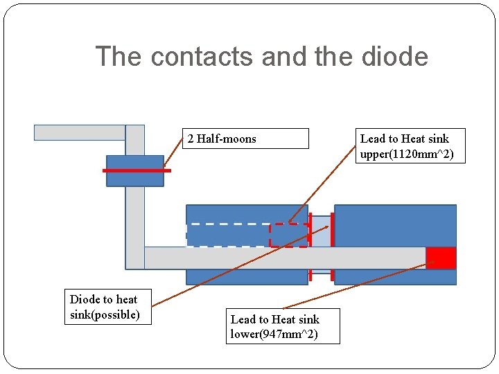
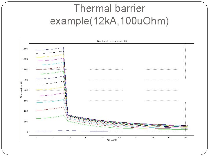
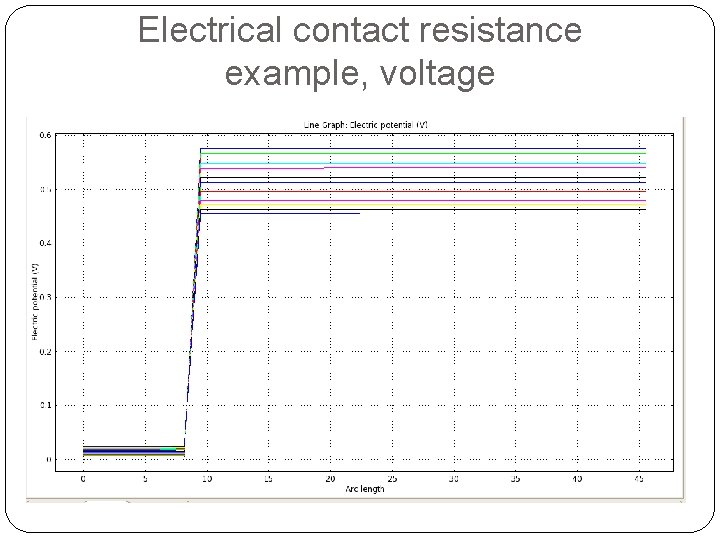
Contact resistances In the lead to heat sink or in the half-moons Different values have been investigated, to see the maximum temperature Both electrical and thermal contact resistances have been assumed, the latter is still an open question; The thermal conductivity of the contact is obtained from Wiedemann-Franz law (proportional to electrical conductivity) Voltages compared to latest measurements, the conclusion is that the observed behavior is the result of more complex phenomena, although contact resistance

The contacts and the diode 2 Half-moons Diode to heat sink(possible) Lead to Heat sink lower(947 mm^2) Lead to Heat sink upper(1120 mm^2)

Thermal barrier example(12 k. A, 100 u. Ohm)

Electrical contact resistance example, voltage

Results for contact resistances

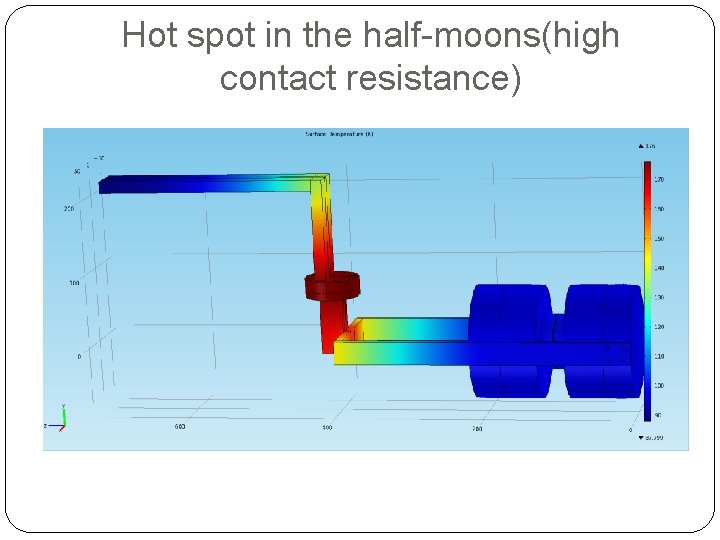
Hot spot in the half-moons(high contact resistance)

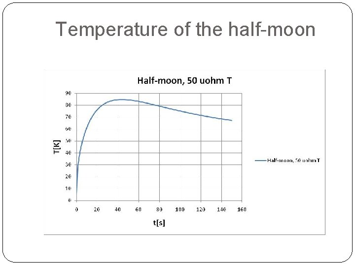
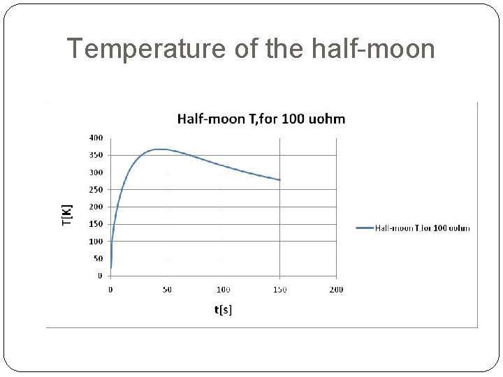
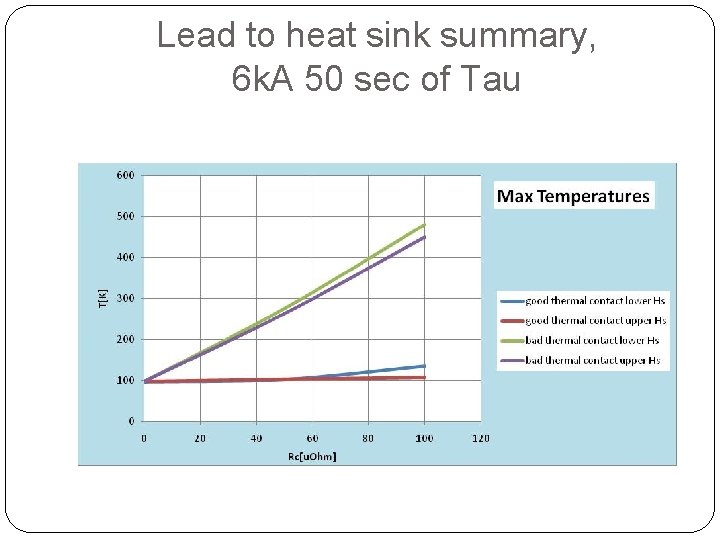
Half moon contacts, 6 k. A 50 sec of Tau

Temperature of the half-moon

Temperature of the half-moon

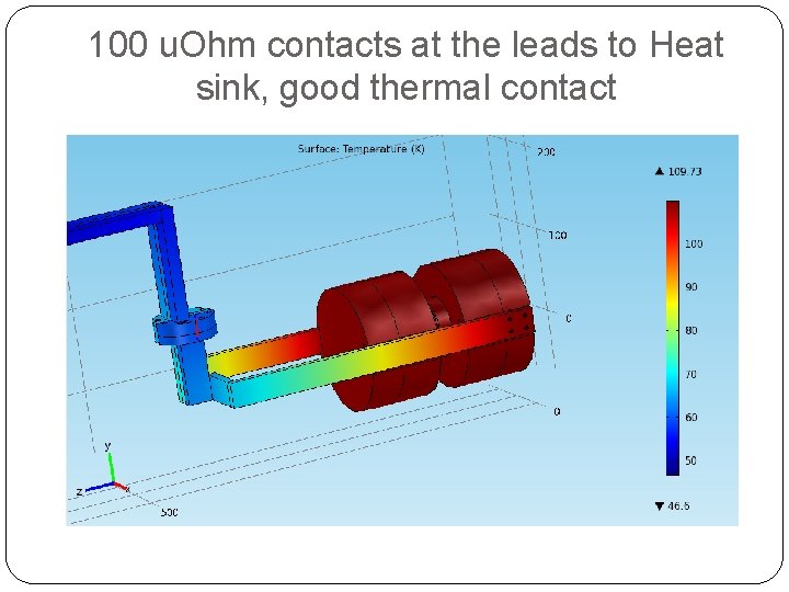
100 u. Ohm contacts at the leads to Heat sink, good thermal contact

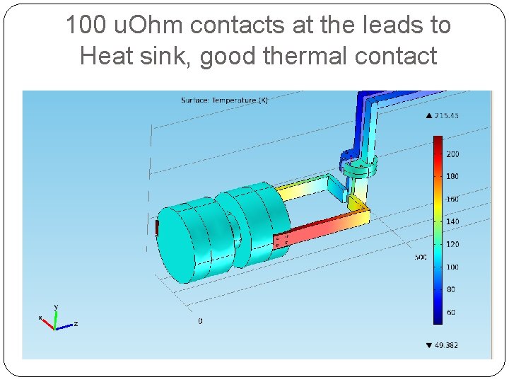
100 u. Ohm contacts at the leads to Heat sink, good thermal contact

Lead to heat sink summary, 6 k. A 50 sec of Tau

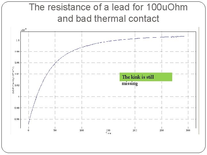
The resistance of a lead for 100 u. Ohm and bad thermal contact The kink is still missing

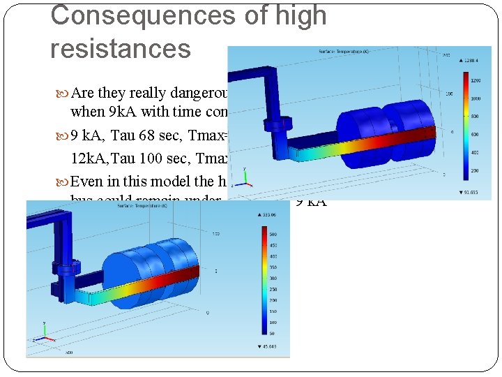
Consequences of high resistances Are they really dangerous? : Yes, even now, but more over when 9 k. A with time constant of 68 sec, or for 12 k. A 100 sec 9 k. A, Tau 68 sec, Tmax=1200 K 12 k. A, Tau 100 sec, Tmax=2500 K (!) Even in this model the hot spot is a very local property, so the bus could remain under 100 K for 9 k. A

Other effects

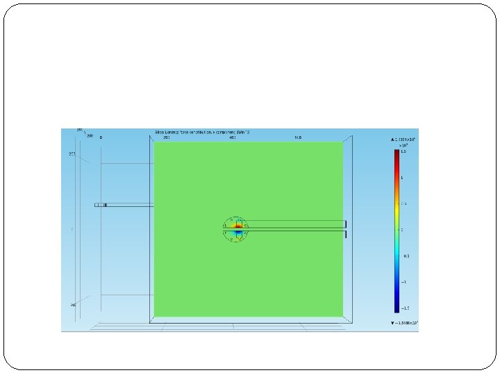
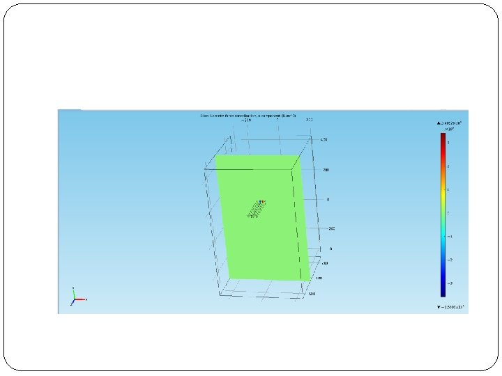
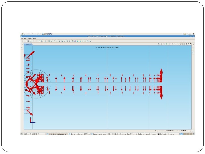
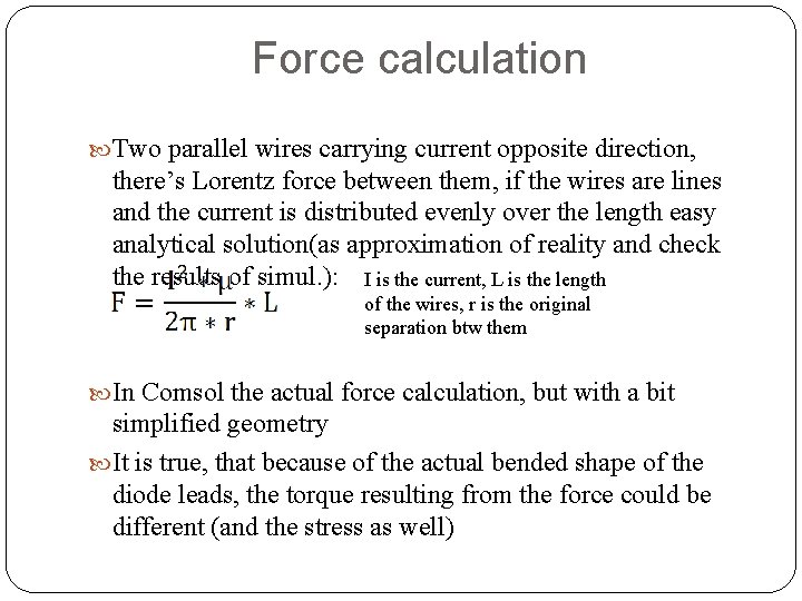
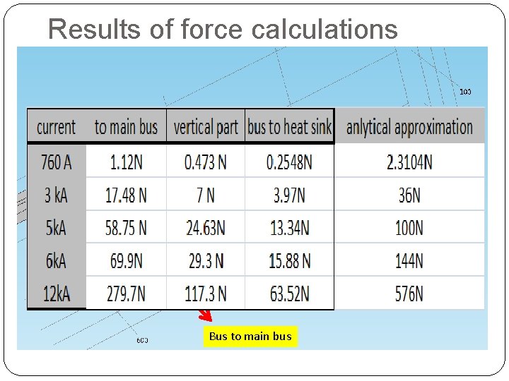
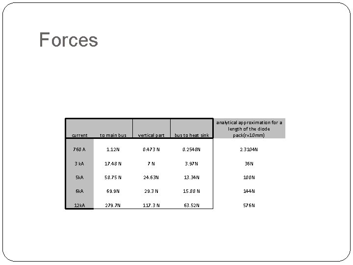
Force calculation Two parallel wires carrying current opposite direction, there’s Lorentz force between them, if the wires are lines and the current is distributed evenly over the length easy analytical solution(as approximation of reality and check the results of simul. ): I is the current, L is the length of the wires, r is the original separation btw them In Comsol the actual force calculation, but with a bit simplified geometry It is true, that because of the actual bended shape of the diode leads, the torque resulting from the force could be different (and the stress as well)

Results of force calculations Vertical part Bus to heat sink Bus to main bus

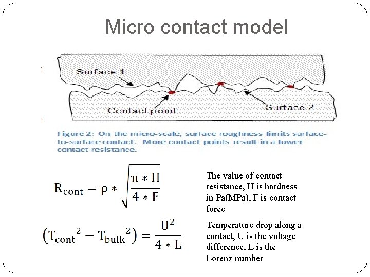
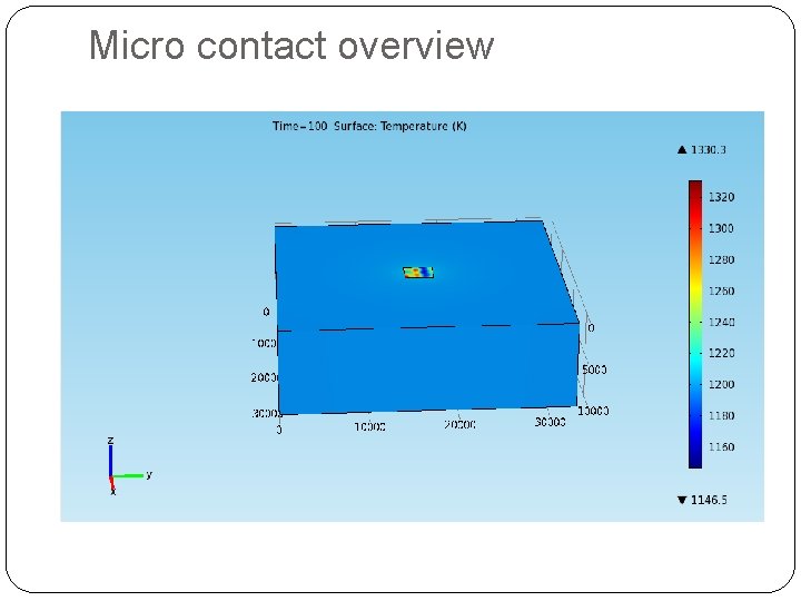
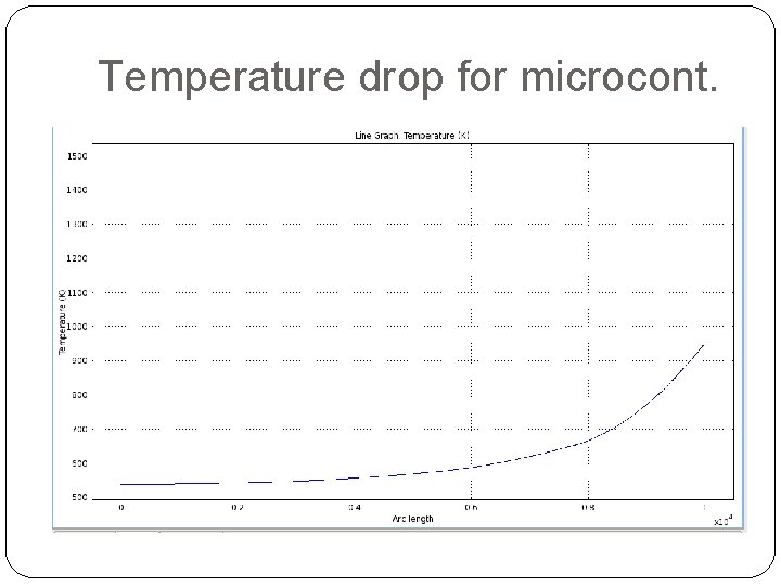
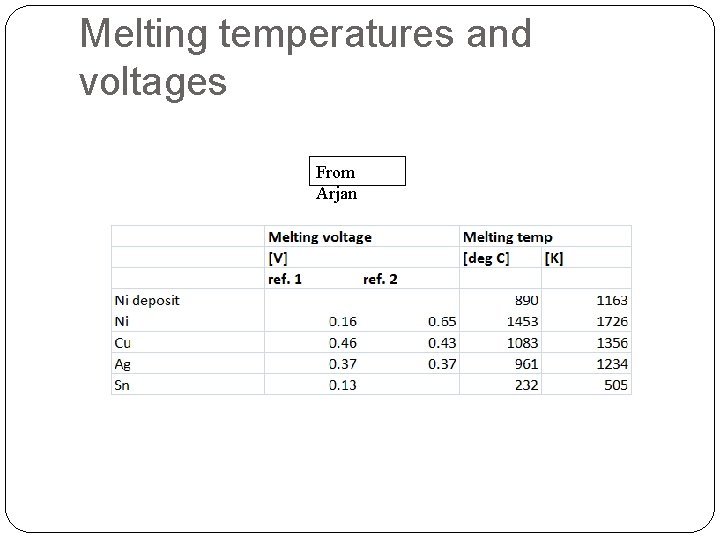
Micro contact model In reality there’s a 2 micron thick Ni coating layer on the Cu elements(probably anti corrision) , and in the half-moon one part is coated by Ag One can find nice formulas for the voltage difference and the temperature of the bulk and the actual hot spots, also for the value of the contact resistance The value of contact resistance, H is hardness in Pa(MPa), F is contact force Temperature drop along a contact, U is the voltage difference, L is the Lorenz number

Micro contact overview

Temperature drop for microcont.

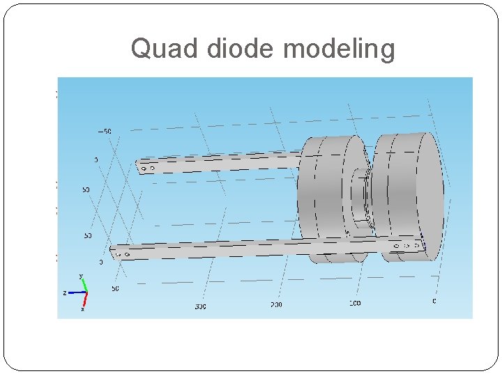
Quad diode modeling They’re quite similar, except a few things: the diode leads are straight (smaller bolts, and bus), no halfmoon less contact surface and the heat sinks are smaller as well (less energy dissipated) For the contacts we can say the same on micro level Similar measured data, except the very steep, step in voltage For the later a possible guess is now being investigated: the moving of the contacts, and after the bolts carrying the current

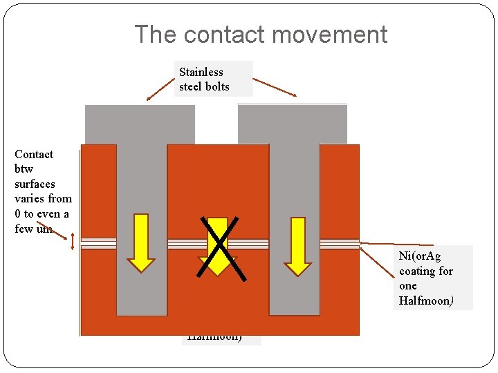
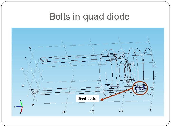
The contact movement Stainless steel bolts Contact btw surfaces varies from 0 to even a few um Cu of Lead (or one Halfmoon) Cu of Heatsink (or one Halfmoon) Ni(or. Ag coating for one Halfmoon)

Some possible explanations Probably we observe these voltages(resistances) as a result of multiple effects, superimposed on each other, An example: as a result of the repelling force the actual contact force is less, so it causes higher contact resistance, which could lead to high temperatures, and after all it results in lower resistances through the melting of the coating These effects are hard to simulate, and more input data is needed, the best would be an actual metallurgic investigation of the surfaces (for diodes in the machine quite impossible)

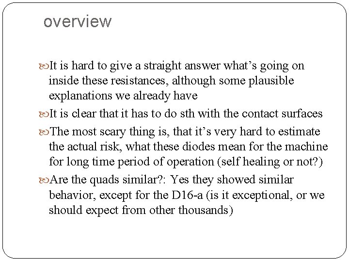
overview It is hard to give a straight answer what’s going on inside these resistances, although some plausible explanations we already have It is clear that it has to do sth with the contact surfaces The most scary thing is, that it’s very hard to estimate the actual risk, what these diodes mean for the machine for long time period of operation (self healing or not? ) Are the quads similar? : Yes they showed similar behavior, except for the D 16 -a (is it exceptional, or we should expect from other thousands)

Backup slides

Bolts in quad diode Steel bolts

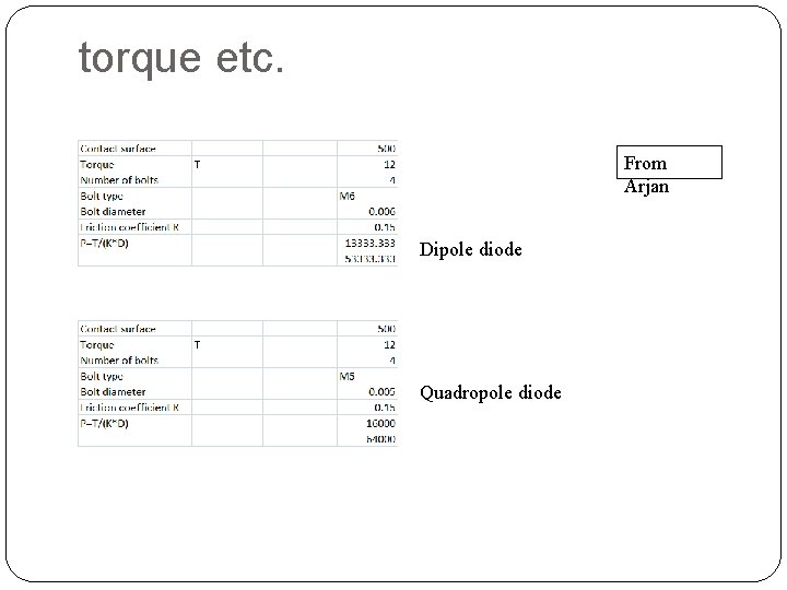
torque etc. From Arjan Dipole diode Quadropole diode

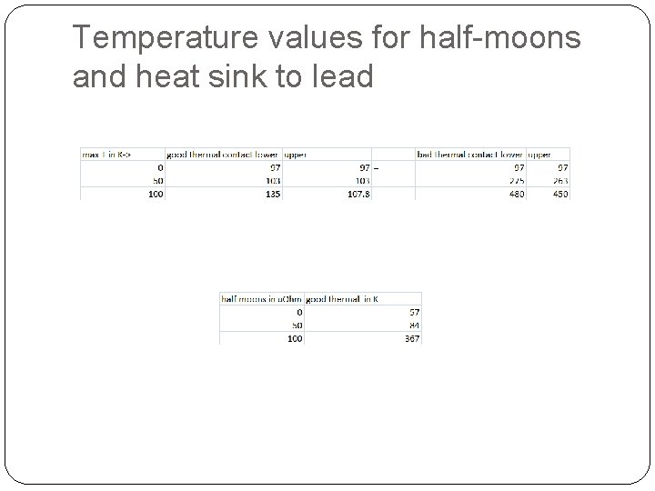
Temperature values for half-moons and heat sink to lead

Forces current to main bus vertical part bus to heat sink analytical approximation for a length of the diode pack(r=10 mm) 760 A 1. 12 N 0. 473 N 0. 2548 N 2. 3104 N 3 k. A 17. 48 N 7 N 3. 97 N 36 N 5 k. A 58. 75 N 24. 63 N 13. 34 N 100 N 6 k. A 69. 9 N 29. 3 N 15. 88 N 144 N 12 k. A 279. 7 N 117. 3 N 63. 52 N 576 N

Melting temperatures and voltages From Arjan

Physical description 46

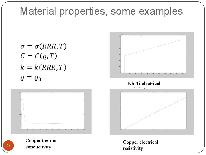
Material properties, some examples Nb-Ti electrical resistivity 47 Copper thermal conductivity Copper electrical resistivity

Comsol 4. 1
