Digital Systems Department of Computer Science and Information

- Slides: 42

數位系統 Digital Systems Department of Computer Science and Information Engineering, Chaoyang University of Technology 朝陽科技大學資 系 Speaker: Fuw-Yi Yang 楊伏夷 伏夷非征番, 道德經 察政章(Chapter 58) 伏者潛藏也 道紀章(Chapter 14) 道無形象, 視之不可見者曰夷 Fuw-Yi Yang 1

Text Book: Digital Design 5 th Ed. Chap 7 Memory and Programmable Logic 7. 1 Introduction 7. 2 Random-Access Memory 7. 3 Memory Decoding 7. 4 Error Detection and Correction 7. 5 Read-Only memory 7. 6 Programmable Logic Array 7. 7 Programmable Array Logic 7. 8 Sequential Programmable Devices Fuw-Yi Yang 2

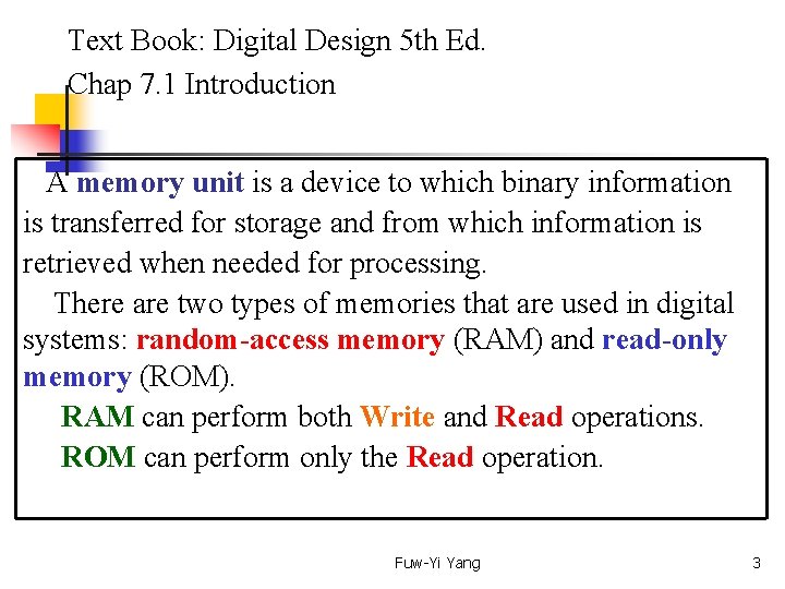
Text Book: Digital Design 5 th Ed. Chap 7. 1 Introduction A memory unit is a device to which binary information is transferred for storage and from which information is retrieved when needed for processing. There are two types of memories that are used in digital systems: random-access memory (RAM) and read-only memory (ROM). RAM can perform both Write and Read operations. ROM can perform only the Read operation. Fuw-Yi Yang 3

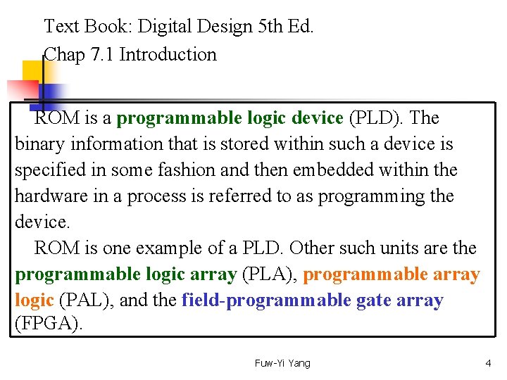
Text Book: Digital Design 5 th Ed. Chap 7. 1 Introduction ROM is a programmable logic device (PLD). The binary information that is stored within such a device is specified in some fashion and then embedded within the hardware in a process is referred to as programming the device. ROM is one example of a PLD. Other such units are the programmable logic array (PLA), programmable array logic (PAL), and the field-programmable gate array (FPGA). Fuw-Yi Yang 4

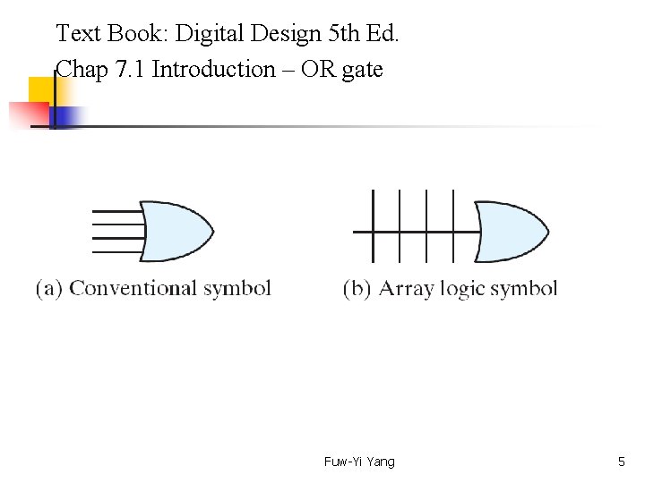
Text Book: Digital Design 5 th Ed. Chap 7. 1 Introduction – OR gate Fuw-Yi Yang 5

Text Book: Digital Design 5 th Ed. Chap 7. 2 Random-Access Memory A memory unit is a collection of storage cells, together with associated circuits needed to transfer into and out of device. The architecture of memory is such that information can be selectively retrieved from any of its internal locations. The time it takes to transfer information to or from any desired random location is always the same – hence the name random access memory. A memory unit stores binary information in groups of bits called words. A group of 8 bits is called a byte. Fuw-Yi Yang 6

Text Book: Digital Design 5 th Ed. Chap 7. 2 Random-Access Memory Integrated circuit RAM units are available in two operating modes: static and dynamic. Static RAM (SRAM) consists essentially of internal latches that store the binary information. Dynamic RAM (DRAM) stores the binary information in the form of electric charges on capacitors provided inside the chip by MOS transistors (require refreshing). Fuw-Yi Yang 7

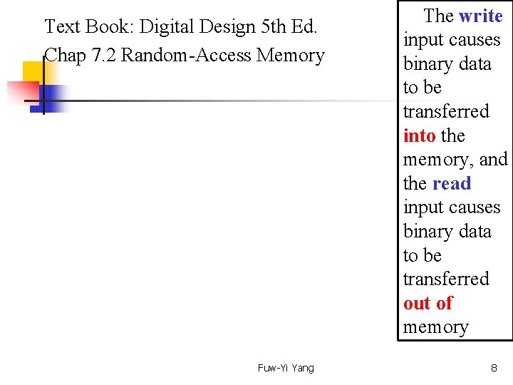
Text Book: Digital Design 5 th Ed. Chap 7. 2 Random-Access Memory Fuw-Yi Yang The write input causes binary data to be transferred into the memory, and the read input causes binary data to be transferred out of memory 8

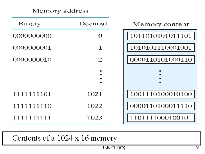
Text Book: Digital Design 4 th Ed. Chap 7. 2 Random-Access Memory Contents of a 1024 x 16 memory Fuw-Yi Yang 9

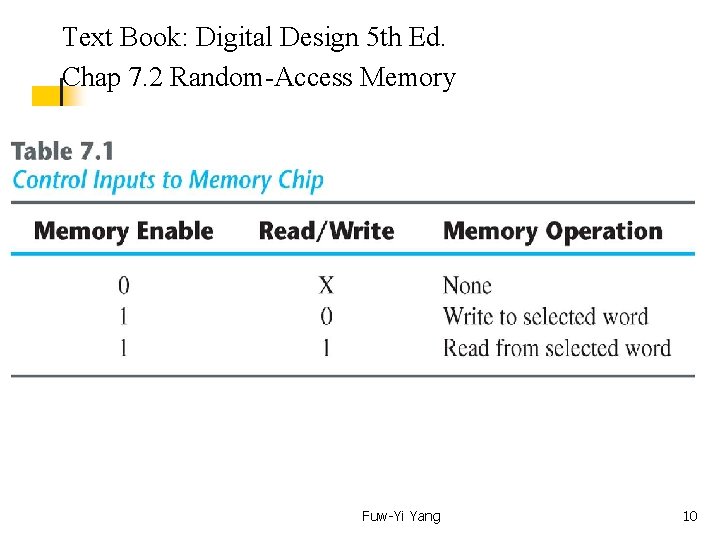
Text Book: Digital Design 5 th Ed. Chap 7. 2 Random-Access Memory Fuw-Yi Yang 10

Text Book: Digital Design 4 th Ed. Chap 7. 2 Random-Access Memory Fuw-Yi Yang 11

Text Book: Digital Design 4 th Ed. Chap 7. 2 Random-Access Memory Fuw-Yi Yang 12

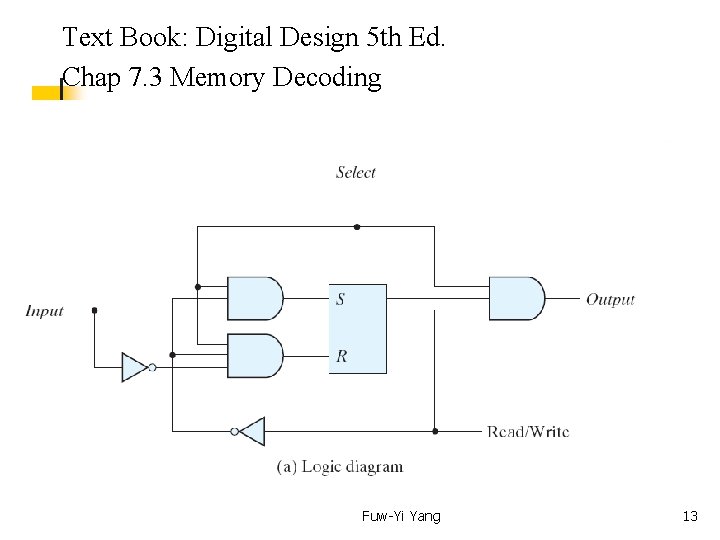
Text Book: Digital Design 5 th Ed. Chap 7. 3 Memory Decoding Fuw-Yi Yang 13

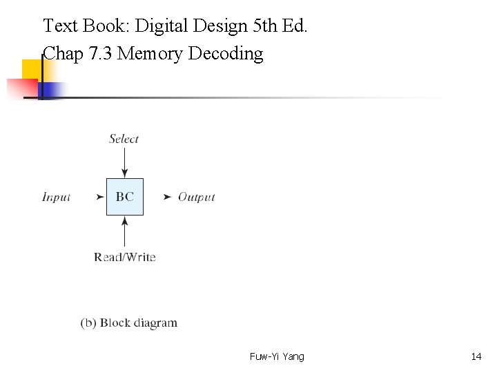
Text Book: Digital Design 5 th Ed. Chap 7. 3 Memory Decoding Fuw-Yi Yang 14

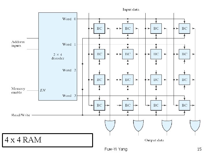
Text Book: Digital Design 4 th Ed. Chap 7. 3 Memory Decoding 4 x 4 RAM Fuw-Yi Yang 15

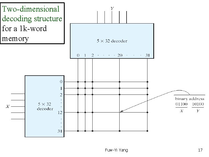
Text Book: Digital Design 5 th Ed. Chap 7. 3 Memory Decoding – Coincident Decoding A decoder with k inputs and 2 k outputs requires 2 k AND gates with k inputs per gate. The total number of gates and the number of inputs per gate can be reduced by employing two decoders in a twodimensional selection scheme. In this configuration, two k/2 -input decoder are used instead of one k-input decoder. (next page). Fuw-Yi Yang 16

Two-dimensional Text Book: Digital Design 4 th Ed. decoding structure Chap 7. 3 Memory Decoding – Coincident Decoding for a 1 k-word memory Fuw-Yi Yang 17

Text Book: Digital Design 4 th Ed. Chap 7. 3 Memory Decoding – Coincident Decoding Address multiplexing for a 64 k DRAM (8 pins for 16 bits address) Fuw-Yi Yang 18

Text Book: Digital Design 5 th Ed. Chap 7. 4 Error detection and correction Fuw-Yi Yang 19

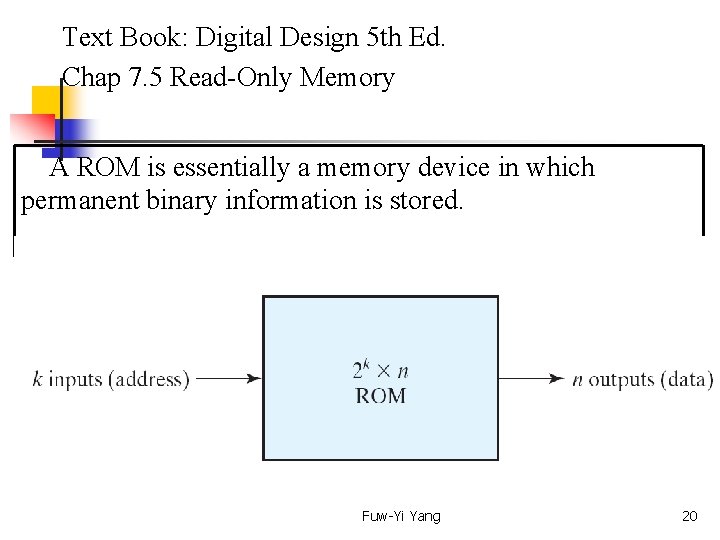
Text Book: Digital Design 5 th Ed. Chap 7. 5 Read-Only Memory A ROM is essentially a memory device in which permanent binary information is stored. Fuw-Yi Yang 20

Text Book: Digital Design 4 th Ed. Chap 7. 5 Read-Only Memory Internal logic of a 32 x 8 ROM Fuw-Yi Yang 21

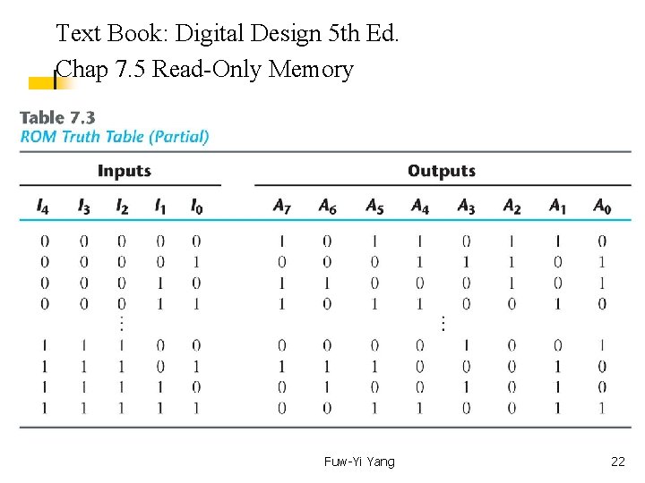
Text Book: Digital Design 5 th Ed. Chap 7. 5 Read-Only Memory Fuw-Yi Yang 22

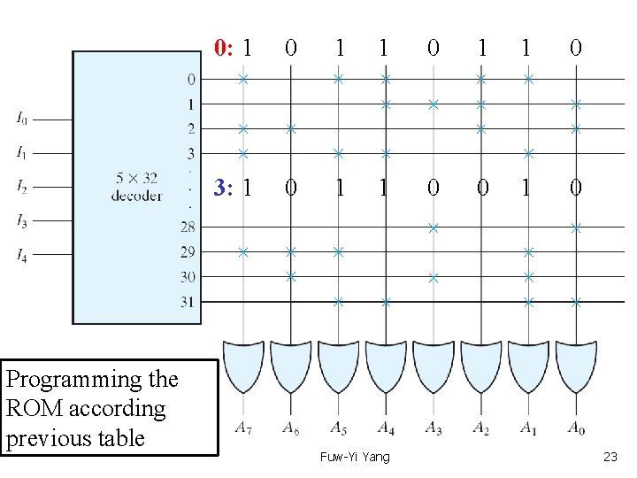
Text Book: Digital Design 4 th Ed. 0: 1 0 1 1 0 Chap 7. 5 Read-Only Memory 3: 1 0 1 1 0 0 1 0 Programming the ROM according previous table Fuw-Yi Yang 23

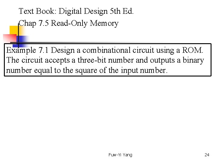
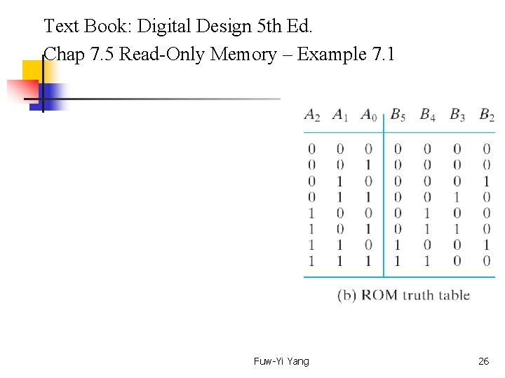
Text Book: Digital Design 5 th Ed. Chap 7. 5 Read-Only Memory Example 7. 1 Design a combinational circuit using a ROM. The circuit accepts a three-bit number and outputs a binary number equal to the square of the input number. Fuw-Yi Yang 24

Text Book: Digital Design 5 th Ed. Chap 7. 5 Read-Only Memory – Example 7. 1 Fuw-Yi Yang 25

Text Book: Digital Design 5 th Ed. Chap 7. 5 Read-Only Memory – Example 7. 1 Fuw-Yi Yang 26

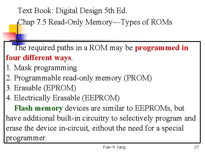
Text Book: Digital Design 5 th Ed. Chap 7. 5 Read-Only Memory—Types of ROMs The required paths in a ROM may be programmed in four different ways. 1. Mask programming 2. Programmable read-only memory (PROM) 3. Erasable (EPROM) 4. Electrically Erasable (EEPROM) Flash memory devices are similar to EEPROMs, but have additional built-in circuitry to selectively program and erase the device in-circuit, eithout the need for a special programmer. Fuw-Yi Yang 27

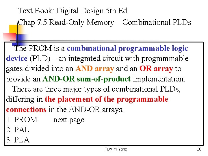
Text Book: Digital Design 5 th Ed. Chap 7. 5 Read-Only Memory—Combinational PLDs The PROM is a combinational programmable logic device (PLD) – an integrated circuit with programmable gates divided into an AND array and an OR array to provide an AND-OR sum-of-product implementation. There are three major types of combinational PLDs, differing in the placement of the programmable connections in the AND-OR arrays. 1. PROM next page 2. PAL 3. PLA Fuw-Yi Yang 28

Text Book: Digital Design 4 th Ed. Chap 7. 5 Read-Only Memory—Combinational PLDs Fuw-Yi Yang 29

Text Book: Digital Design 5 th Ed. Chap 7. 6 Programmable Logic Array The PLA is similar in concept to the PROM, except that the PLA does not provide fully decoding of the variables and does not generate all the minterms. Fuw-Yi Yang 30

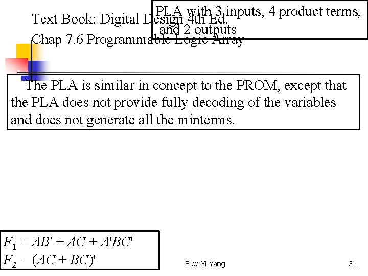
PLA with 3 inputs, 4 product terms, Text Book: Digital Design 4 th Ed. and 2 outputs Chap 7. 6 Programmable Logic Array The PLA is similar in concept to the PROM, except that the PLA does not provide fully decoding of the variables and does not generate all the minterms. F 1 = AB' + AC + A'BC' F 2 = (AC + BC)' Fuw-Yi Yang 31

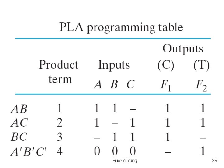
F 1 = AB' + AC + A'BC' Text Book: Digital Design 4 th Ed. F 2 = (AC + BC)' Chap 7. 6 Programmable Logic Array Fuse map of F 1 and F 2 specified in a tabular form Fuw-Yi Yang 32

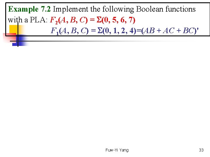
Example 7. 2 Implement the following Boolean functions with a PLA: F 2(A, B, C) = (0, 5, 6, 7) F 1(A, B, C) = (0, 1, 2, 4)=(AB + AC + BC)' Fuw-Yi Yang 33

Text Book: Digital Design 5 th Ed. Chap 7. 7 Programmable Array Logic PAL The PAL is a programmable logic device with a fixed OR array and programmable AND array. Fuw-Yi Yang 34

Text Book: Digital Design 4 th Ed. Chap 7. 7 Programmable Array Logic PAL The PAL is a programmable logic device with a fixed OR array and programmable AND array. Fuw-Yi Yang 35

Text Book: Digital Design 4 th Ed. Chap 7. 7 Programmable Array Logic PAL Fuw-Yi Yang 36

Text Book: Digital Design 4 th Ed. Chap 7. 7 Programmable Array Logic PAL The PAL is a programmable logic device with a fixed OR array and programmable AND array. Fuw-Yi Yang 37

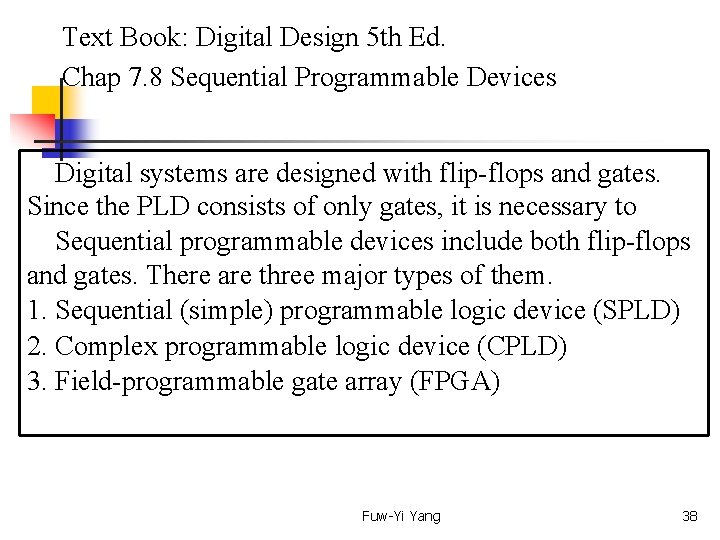
Text Book: Digital Design 5 th Ed. Chap 7. 8 Sequential Programmable Devices Digital systems are designed with flip-flops and gates. Since the PLD consists of only gates, it is necessary to Sequential programmable devices include both flip-flops and gates. There are three major types of them. 1. Sequential (simple) programmable logic device (SPLD) 2. Complex programmable logic device (CPLD) 3. Field-programmable gate array (FPGA) Fuw-Yi Yang 38

Text Book: Digital Design 5 th Ed. Chap 7. 8 Sequential Programmable Devices Sequential Programmable logic device Fuw-Yi Yang 39

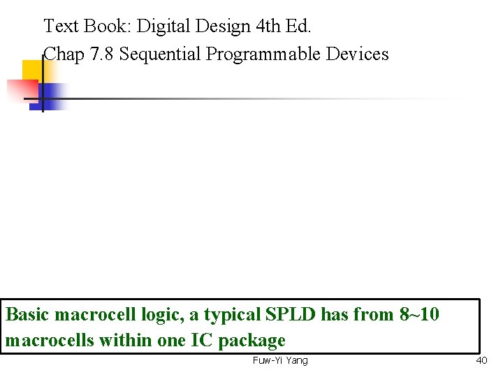
Text Book: Digital Design 4 th Ed. Chap 7. 8 Sequential Programmable Devices Basic macrocell logic, a typical SPLD has from 8~10 macrocells within one IC package Fuw-Yi Yang 40

Text Book: Digital Design 4 th Ed. Chap 7. 8 Sequential Programmable Devices General CPLD configuration Fuw-Yi Yang 41

Text Book: Digital Design 4 th Ed. Chap 7. 8 Sequential Programmable Devices General CPLD configuration Fuw-Yi Yang 42