Digital Systems Combinational Logic Circuits WenHung Liao Ph
Digital Systems: Combinational Logic Circuits Wen-Hung Liao, Ph. D.
Objectives l l l Convert a logic expression into a sum-of-products expression. Perform the necessary steps to reduce a sum-ofproducts expression to its simplest form. Use Boolean algebra and the Karnaugh map as tools to simplify and design logic circuits. Explain the operation of both exclusive-OR and exclusive-NOR circuits. Design simple logic circuits without the help of a truth table.
Objectives (cont’d) l l l Implement enable circuits. Cite the basic characteristics of TTL and CMOS digital ICs. Use the basic troubleshooting rules of digital systems. Deduce from observed results the faults of malfunctioning combinational logic circuits. Describe the fundamental idea of programmable logic devices (PLDs). Outline the steps involved in programming a PLD to perform a simple combinational logic function
Combinational Logic Circuits l l l The logic level at the output depends on the combination of logic levels present at the inputs. A combinational circuit has no memory, so its output depends only on the current value of its inputs. We will not spend a great deal of time discussing how to troubleshoot the combinational circuits. (That’s what the lab is for. )
Sum-of-Products Form l l l Sum OR Product AND Each of the sum-of-products expression consists of two or more AND terms that are ORed together. Examples: ABC+A’BC’ AB+A’BC’+C’D’+D Note that one inversion sign cannot cover more than one variable in a term. AB is not allowed.
Product-of-Sums Form l l l Each of the product-of-sums expression consists of two or more OR terms that are ANDed together. Examples: (A+B’+C)(A+C) (A+B’)(C’+D)F Will use sum-of-products form in logic circuit simplification.
Simplifying Logic Circuits l l Goal: reduce the logic circuit expression to a simpler form so that fewer gates and connections are required to build the circuit. Example: 4. 1(a) and 4. 1(b) are equivalent, but 4 -1(b) is much simpler.
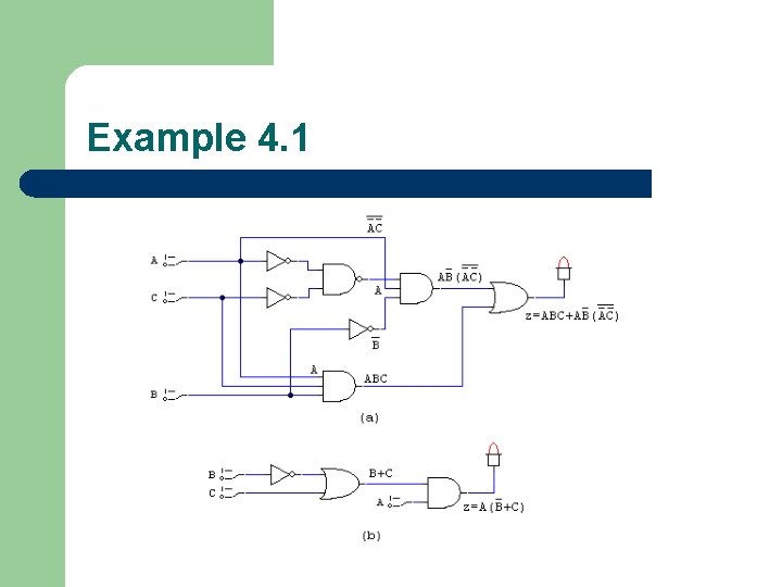
Example 4. 1
Circuit Simplification Methods l l l Boolean algebra: greatly depends on inspiration and experience. Karnaugh map: systematic, step-by-step approach. Pros and Cons
Algebraic Simplification l l l Use the Boolean algebra theorems introduced in Chapter 3 to help simplify the expression for a logic circuit. Based on experience, often becomes a trialand-error process. No easy way to tell whether a simplified expression is in its simplest form.
Two Essential Steps l l The original expression is put into the sum-ofproducts form by repeated application of De. Morgan’s theorem and multiplication of terms. The product terms are checked for common factors, and factoring is performed whenever possible.
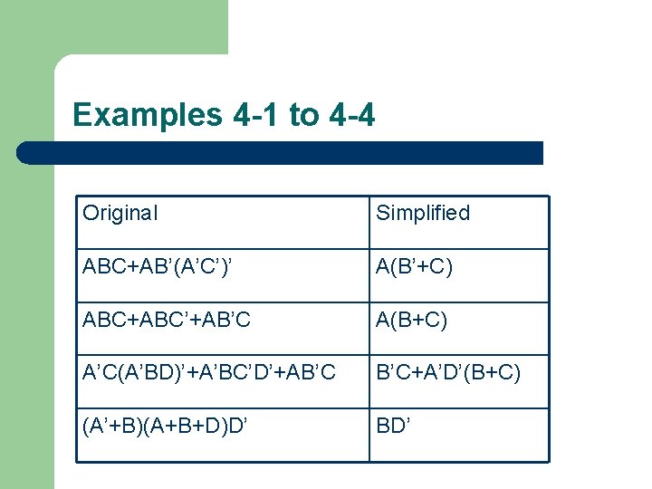
Examples 4 -1 to 4 -4 Original Simplified ABC+AB’(A’C’)’ A(B’+C) ABC+ABC’+AB’C A(B+C) A’C(A’BD)’+A’BC’D’+AB’C B’C+A’D’(B+C) (A’+B)(A+B+D)D’ BD’
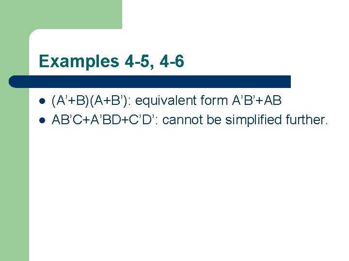
Examples 4 -5, 4 -6 l l (A’+B)(A+B’): equivalent form A’B’+AB AB’C+A’BD+C’D’: cannot be simplified further.
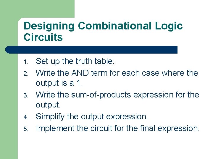
Designing Combinational Logic Circuits 1. 2. 3. 4. 5. Set up the truth table. Write the AND term for each case where the output is a 1. Write the sum-of-products expression for the output. Simplify the output expression. Implement the circuit for the final expression.
Example 4 -8 l Design a logic circuit that is to produce a HIGH output when the voltage (represented by a fourbit binary number ABCD) is greater than 6 V.
Example 4 -9 l Generate the STOP signal and energize an indicator light whenever either of the following conditions exists: (1) there is no paper in the paper feeder tray; or (2) the two micro-switches in the paper path are activated, indicating a jam.
Karnaugh Map Method l l A graphical device to simplify a logic expression. Will only work on examples with up to 4 input variables. From truth table to logic expression to K map. Figure 4. 11 shows the K map with 2, 3 and 4 variables.
Looping l l l The expression for output X can be simplified by properly combining those squares in the K map which contain 1 s. The process of combining these 1 s is called looping. Looping groups of two (pairs) eliminate 1 variable Looping groups of four (quads) eliminate 2 variables Looping groups of eight (octets) eliminate 3 variables See Figure 4 -12 to 4 -14.
Complete Simplification Process l l Step 1: Construct the K map and places 1 s in those squares corresponding to the 1 s in the truth table. Places 0 s in the other squares. Step 2: Examine the map for adjacent 1 s and loop those 1 s which are not adjacent to any other 1 s. (isolated 1 s) Step 3: Look for those 1 s which are adjacent to only one other 1. Loop any pair containing such a 1. Step 4: Loop any octet even when it contains some 1 s that have already been looped.
Complete Simplification Process l l l Step 5: Loop any quad that contains one or more 1 s that have not already been looped, making sure to use the minimum number of loops. Step 6: Loop any pairs necessary to include any 1 s have not already been looped, making sure to use the minimum number of loops. Step 7: Form the ORed sum of all the terms generated by each loop.
Filling K Map from Output Expression l l What to do when the desired output is presented as a Boolean expression instead of a truth table? Step 1: Convert the expression into SOP form. Step 2: For each product term in the SOP expression, place a 1 in each K-map square whose label contains the same combination of input values. Place a 0 in other squares. Example 4 -14: y=C’(A’B’D’+D)+AB’C+D’
Don’t-Care Conditions l l l Some logic circuits can be designed so that there are certain input conditions for which there are no specified output levels. A circuit designer is free to make the output for any don’t care condition either a 0 or a 1 in order to produce the simplest output expression. Figures 4 -18, 19.
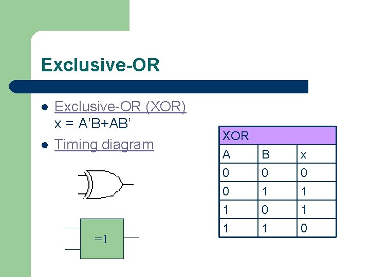
Exclusive-OR l l Exclusive-OR (XOR) x = A’B+AB’ Timing diagram =1 XOR A B x 0 0 0 1 1 1 0
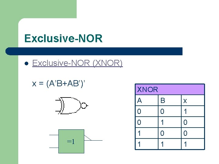
Exclusive-NOR l Exclusive-NOR (XNOR) x = (A’B+AB’)’ =1 XNOR A B x 0 0 0 1 1 0 1
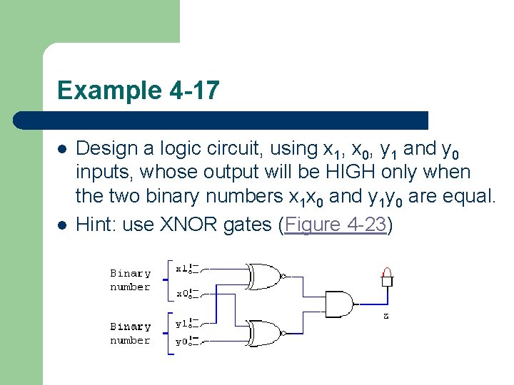
Example 4 -17 l l Design a logic circuit, using x 1, x 0, y 1 and y 0 inputs, whose output will be HIGH only when the two binary numbers x 1 x 0 and y 1 y 0 are equal. Hint: use XNOR gates (Figure 4 -23)
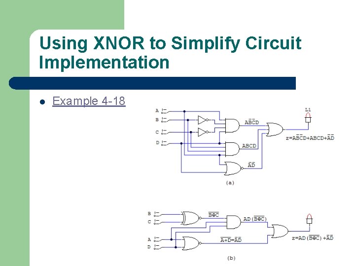
Using XNOR to Simplify Circuit Implementation l Example 4 -18
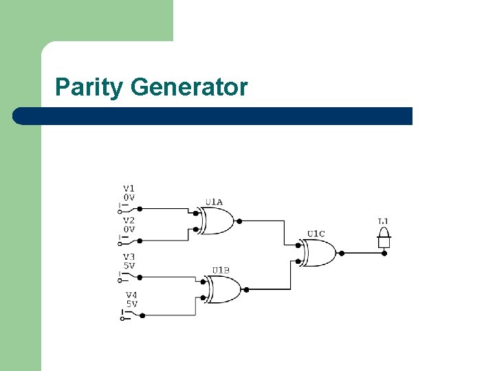
Parity Generator
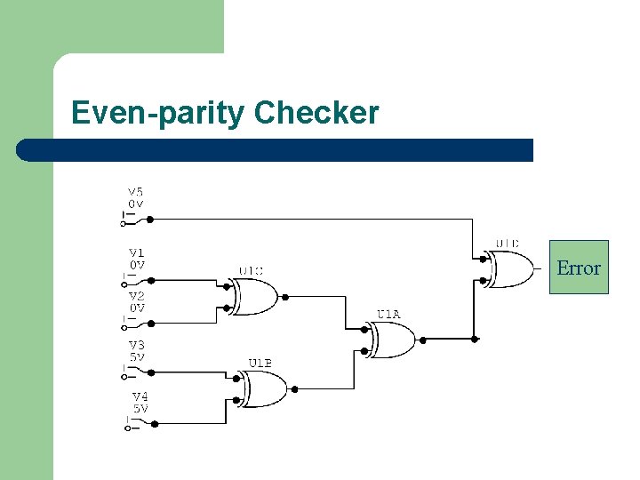
Even-parity Checker Error
Enable/Disable Circuits l l l Each of the basic logic gates can be used to control the passage of an input logic signal through to the output. A: input, B: control (Figure 4 -26) The logic level at the control input determines whether the input signal is enabled to reach the output or disabled from reaching the output.
Basic Characteristics of Digital ICs l l l Digital ICs are a collection of resistors, diodes and transistor fabricated on a single piece of semiconductor material called a substrate, which is commonly referred to as a chip. The chip is enclosed in a package. Dual-in-line package (DIP)
Integrated Circuits Complexity Number of Gates Small-scale integration(SSI) <12 Medium-scale integration(MSI) 12 to 99 Large-scale integration(LSI) 100 to 9999 Very large-scale integration(VLSI) 10, 000 to 99, 999 Ultra large-scale integration(ULSI) 100, 000 to 999, 999 Giga-scale integration (GSI) 1, 000 or more
Bipolar and Unipolar Digital ICs l l l Categorized according to the principal type of electronic component used in their circuitry. Bipolar ICs are those that are made using the bipolar junction transistor (PNP or NPN). Unipolar ICs are those that use the unipolar field-effect transistors (P-channel and Nchannel MOSFETs).
IC Families l l l TTL Family: bipolar digital ICs (Table 4 -6) CMOS Family: unipolar digital ICs (Table 4 -7) TTL and CMOS dominate the field of SSI and MSI devices.
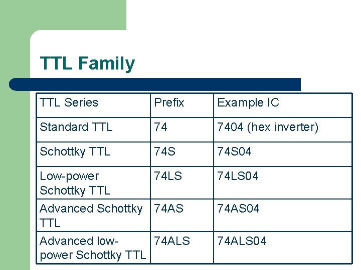
TTL Family TTL Series Prefix Example IC Standard TTL 74 7404 (hex inverter) Schottky TTL 74 S 04 Low-power Schottky TTL 74 LS 04 Advanced Schottky 74 AS TTL Advanced low 74 ALS power Schottky TTL 74 AS 04 74 ALS 04
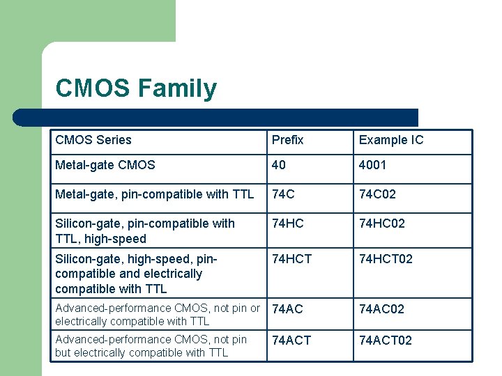
CMOS Family CMOS Series Prefix Example IC Metal-gate CMOS 40 4001 Metal-gate, pin-compatible with TTL 74 C 02 Silicon-gate, pin-compatible with TTL, high-speed 74 HC 02 Silicon-gate, high-speed, pincompatible and electrically compatible with TTL 74 HCT 02 Advanced-performance CMOS, not pin or electrically compatible with TTL 74 AC 02 Advanced-performance CMOS, not pin but electrically compatible with TTL 74 ACT 02
Power and Ground l l l To use digital IC, it is necessary to make proper connection to the IC pins. Power: labeled Vcc for the TTL circuit, labeled VDD for CMOS circuit. Ground
Logic-level Voltage Ranges l l For TTL devices, VCC is normally 5 V. For CMOS circuits, V can range from 3 -18 V. For TTL, logic 0 : 0 -0, 8 V, logic 1: 2 -5 V For CMOS, logic 0 : 0 -1. 5 V, logic 1: 3. 5 -5 V DD
Unconnected Inputs l l l Also called floating inputs. A floating TTL input acts like a logic 1, but measures a DC level of between 1. 4 and 1. 8 V. A CMOS input cannot be left floating.
Logic-Circuit Connection Diagrams l l A connection diagram shows all electrical connections, pin numbers, IC numbers, component values, signal names, and power supply voltages. See Figure 4 -32.
Troubleshooting Digital Systems l l Fault detection Fault isolation Fault correction Good troubleshooting techniques can be learned only through experimentation and actual troubleshooting of faulty circuits.
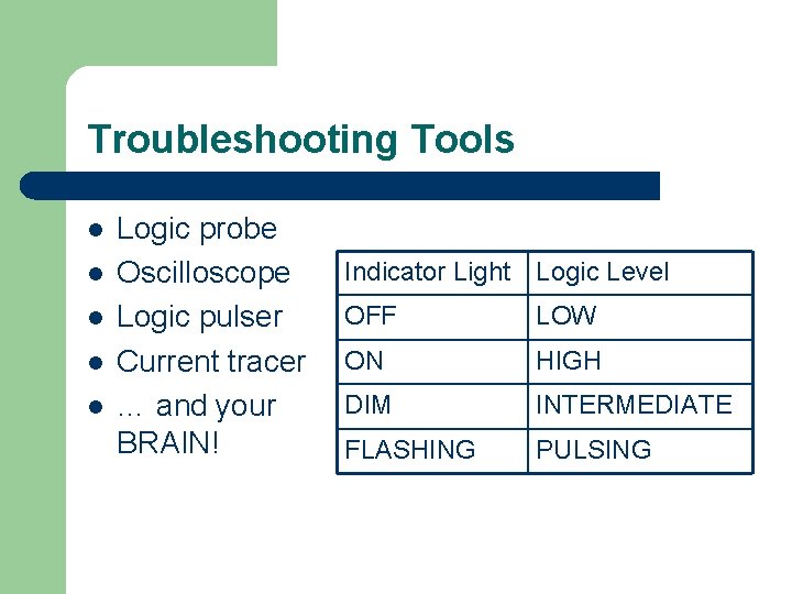
Troubleshooting Tools l l l Logic probe Oscilloscope Logic pulser Current tracer … and your BRAIN! Indicator Light Logic Level OFF LOW ON HIGH DIM INTERMEDIATE FLASHING PULSING
Internal IC Faults l l Malfunction is the internal circuitry. Inputs or outputs shorted to ground or Vcc (Figure 4. 34, 4 -35) Inputs or outputs open-circuited (Figure 4. 36) Short between two pins (other than ground or Vcc): whenever two signals that are supposed to be different show the same logic-level variations.
External Faults l l Open signal lines: Broken wire, Poor solder connection, Crack or cut trace on a printed circuit board, Bend or broken pin on a IC, faulty IC socket. Shorted signal lines: sloppy wiring, solder bridges, incomplete etching. Faulty power supply Output loading: when an output is connected to too many IC inputs.
Programmable Logic Device l l l PLD is an integrated circuit that contains a particular arrangement of logic gates. (Figure 4. 41) Useful in implementing complex circuits containing tens or thousands of logic gates. Sum-of-products form
- Slides: 44