Digital System Verification VERIFICATION OUTLINE Purpose of Verification
- Slides: 23

Digital System Verification

VERIFICATION OUTLINE • Purpose of Verification – Verification effort and cost • Verification Tools – – – Linting tools Code Coverage Simulation Equivalence Checking Rapid Prototyping • Verification Strategy – – Verification plan Directed Testing Constrained-Random Testing Coverage-driven verification • Verification Techniques – Text I/O – Self-checking Testbench – OOP in Testbenches

VERIFICATION (1/2) • The process of demonstrating the functional correctness of a design • For multi-million gate ASICs, So. Cs and reusable IP: – 70% of design effort goes to verification – More (twice as many) verification engineers than designers – Testbench code is 4 times more than RTL code

VERIFICATION (2/2) • It is impossible to prove that a design meets the intent of its specification. • Specification documents are open to interpretation • Functional verification can show that a design meets the intent of its specification, but it cannot prove it. • It can prove that the design does not implement the intended function by identifying a single discrepancy.

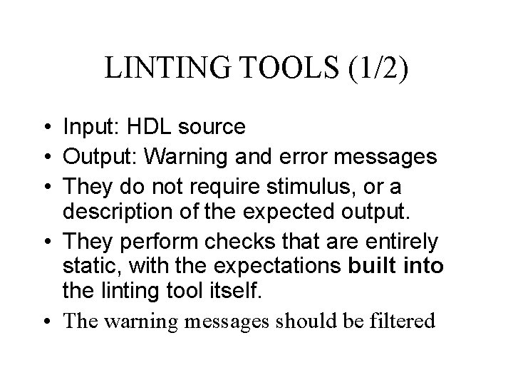
LINTING TOOLS (1/2) • Input: HDL source • Output: Warning and error messages • They do not require stimulus, or a description of the expected output. • They perform checks that are entirely static, with the expectations built into the linting tool itself. • The warning messages should be filtered

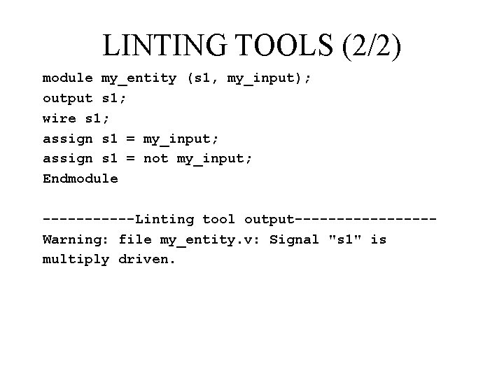
LINTING TOOLS (2/2) module my_entity (s 1, my_input); output s 1; wire s 1; assign s 1 = my_input; assign s 1 = not my_input; Endmodule ------Linting tool output--------Warning: file my_entity. v: Signal "s 1" is multiply driven.

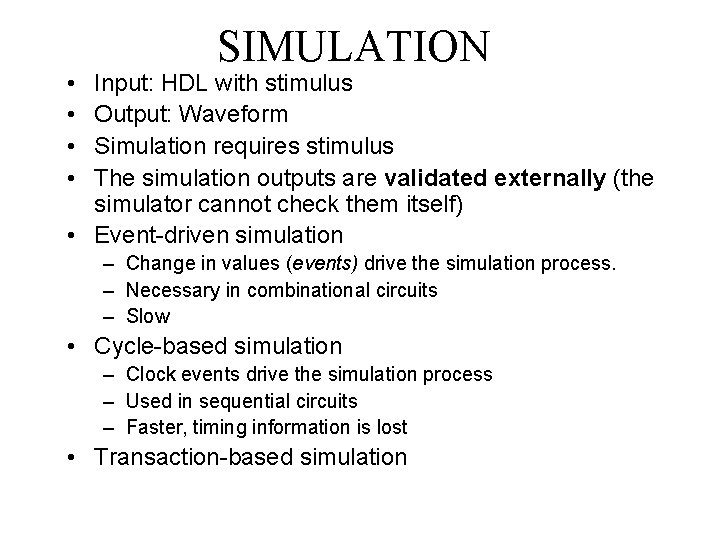
• • SIMULATION Input: HDL with stimulus Output: Waveform Simulation requires stimulus The simulation outputs are validated externally (the simulator cannot check them itself) • Event-driven simulation – Change in values (events) drive the simulation process. – Necessary in combinational circuits – Slow • Cycle-based simulation – Clock events drive the simulation process – Used in sequential circuits – Faster, timing information is lost • Transaction-based simulation

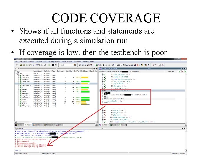
CODE COVERAGE • Shows if all functions and statements are executed during a simulation run • If coverage is low, then the testbench is poor

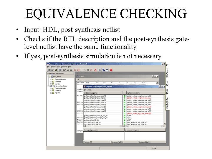
EQUIVALENCE CHECKING • Input: HDL, post-synthesis netlist • Checks if the RTL description and the post-synthesis gatelevel netlist have the same functionality • If yes, post-synthesis simulation is not necessary

RAPID PROTOTYPING • Using FPGAs to create a prototype of the final design • Faster than simulation • The prototype doesn’t have to meet final product constraints (speed, area, power) • Important: Write reusable HDL code to reuse it for the final ASIC product

VERIFICATION PLAN • The verification plan is a specification document for the verification effort • Ad-hoc approaches are inefficient • Define first-time success – Which features are critical and which optional • Define a verification schedule • Specify the features that must be verified – The RTL design team must contribute • Plan how to verify the response – Some responses are difficult to verify visually

VERIFICATION PLAN • A definition of what the design does shall be specified. – input patterns it can handle, – errors it can sustain – based on functional specification document of the design agreed upon by the design and verification teams. • A definition of what the design must not do shall be specified. – The verification requirements must outline which errors to look for. • Any functionality not covered by the verification process shall be defined – The conditions considered to be outside the usage space of the design must be outlined • Each verification requirement must have a unique identifier. • Requirements should be ranked and ordered • Stimulus requirements shall be identified.

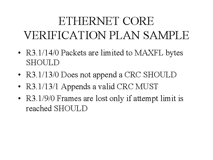
ETHERNET CORE VERIFICATION PLAN SAMPLE • R 3. 1/14/0 Packets are limited to MAXFL bytes SHOULD • R 3. 1/13/0 Does not append a CRC SHOULD • R 3. 1/13/1 Appends a valid CRC MUST • R 3. 1/9/0 Frames are lost only if attempt limit is reached SHOULD

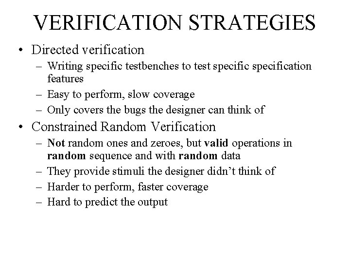
VERIFICATION STRATEGIES • Directed verification – Writing specific testbenches to test specification features – Easy to perform, slow coverage – Only covers the bugs the designer can think of • Constrained Random Verification – Not random ones and zeroes, but valid operations in random sequence and with random data – They provide stimuli the designer didn’t think of – Harder to perform, faster coverage – Hard to predict the output

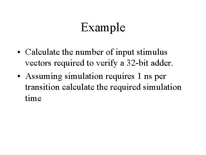
Example • Calculate the number of input stimulus vectors required to verify a 32 -bit adder. • Assuming simulation requires 1 ns per transition calculate the required simulation time

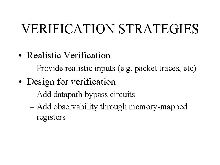
VERIFICATION STRATEGIES • Realistic Verification – Provide realistic inputs (e. g. packet traces, etc) • Design for verification – Add datapath bypass circuits – Add observability through memory-mapped registers

TESTBENCHES • Non-synthesizable code is allowed and, in fact, essential • Do not use RTL code in testbenches

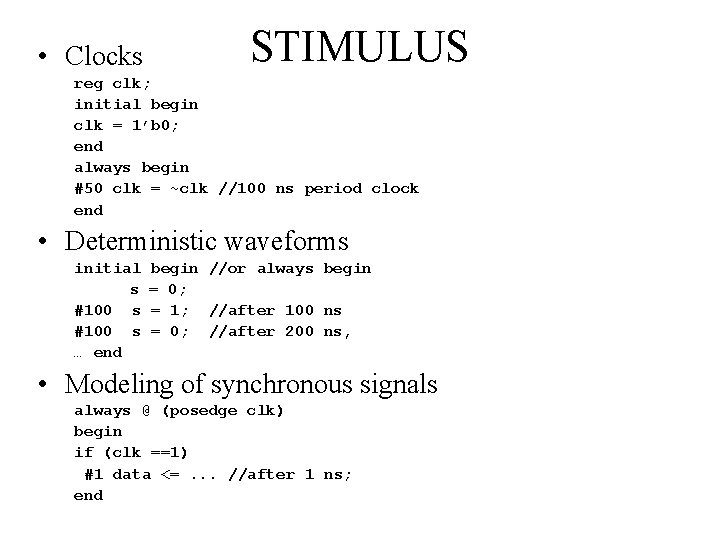
• Clocks STIMULUS reg clk; initial begin clk = 1’b 0; end always begin #50 clk = ~clk //100 ns period clock end • Deterministic waveforms initial s #100 s … end begin //or always begin = 0; = 1; //after 100 ns = 0; //after 200 ns, • Modeling of synchronous signals always @ (posedge clk) begin if (clk ==1) #1 data <=. . . //after 1 ns; end

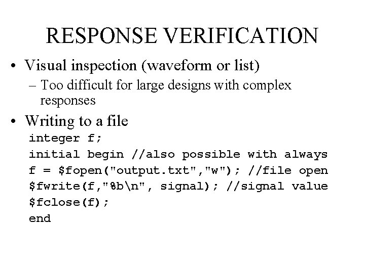
RESPONSE VERIFICATION • Visual inspection (waveform or list) – Too difficult for large designs with complex responses • Writing to a file integer f; initial begin //also possible with always f = $fopen("output. txt", "w"); //file open $fwrite(f, "%bn", signal); //signal value $fclose(f); end

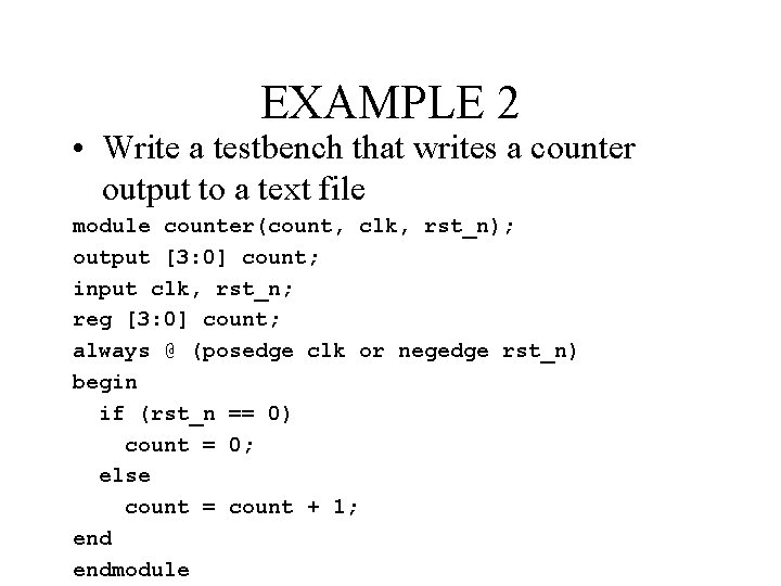
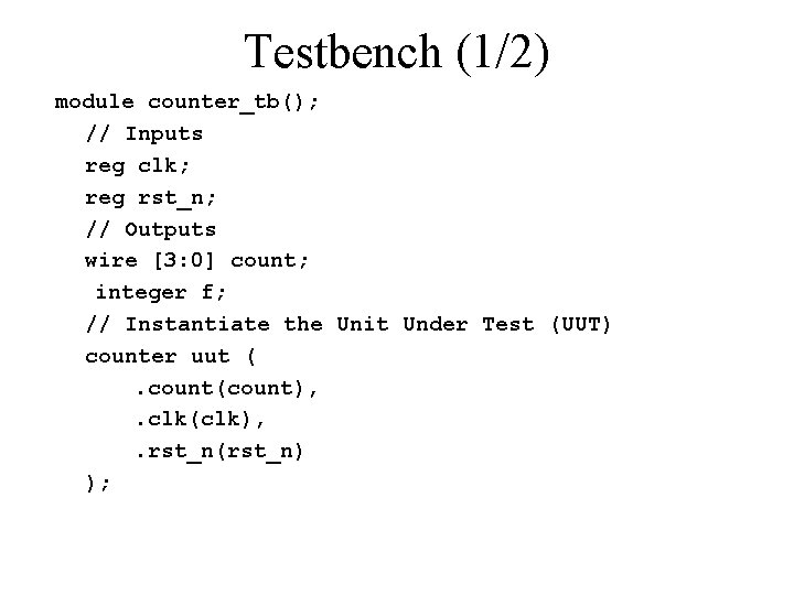
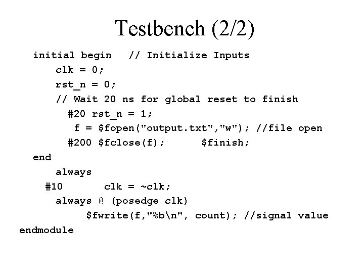
EXAMPLE 2 • Write a testbench that writes a counter output to a text file module counter(count, clk, rst_n); output [3: 0] count; input clk, rst_n; reg [3: 0] count; always @ (posedge clk or negedge rst_n) begin if (rst_n == 0) count = 0; else count = count + 1; endmodule

Testbench (1/2) module counter_tb(); // Inputs reg clk; reg rst_n; // Outputs wire [3: 0] count; integer f; // Instantiate the Unit Under Test (UUT) counter uut (. count(count), . clk(clk), . rst_n(rst_n) );

Testbench (2/2) initial begin // Initialize Inputs clk = 0; rst_n = 0; // Wait 20 ns for global reset to finish #20 rst_n = 1; f = $fopen("output. txt", "w"); //file open #200 $fclose(f); $finish; end always #10 clk = ~clk; always @ (posedge clk) $fwrite(f, "%bn", count); //signal value endmodule

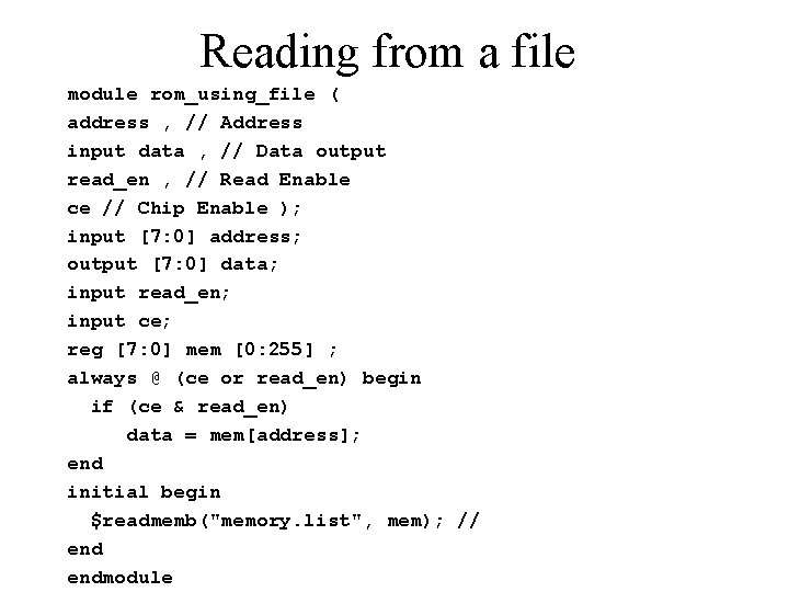
Reading from a file module rom_using_file ( address , // Address input data , // Data output read_en , // Read Enable ce // Chip Enable ); input [7: 0] address; output [7: 0] data; input read_en; input ce; reg [7: 0] mem [0: 255] ; always @ (ce or read_en) begin if (ce & read_en) data = mem[address]; end initial begin $readmemb("memory. list", mem); // endmodule