DIGITAL SYSTEM DESIGN Sub Code 3 EC 4


DIGITAL SYSTEM DESIGN Sub. Code : 3 EC 4 -04 UNIT-2 MSI DEVICES – COMBINATIONAL CIRCUITS By. Neeraj Jain (Assistant Professor) Department of Electronics & Communication Engineering Swami Keshvanand Institute of Technology, Management & Gramothan, Jaipur

Combinational circuits • A combinational logic circuit is one in which the present state of the combination of the logic inputs decides the output. • The term combination logic means combining of two or more logic gates to form a required function where the output at a given time depends only on the input. • The required output data is obtained from this process by transforming the binary information given at the input.

Classification of Combinational Logic

Characterstics: • The output of combinational circuit at any instant of time, depends only on the levels present at input terminals. • The combinational circuit do not use any memory. The previous state of input does not have any effect on the present state of the circuit. • A combinational circuit can have an n number of inputs and m number of outputs.

Logic Gates • Logic gates are the actual physical implementations of the logical operators. • These gates form the basic building blocks for all digital logic circuits. • Logic gates process signals which represent true or false.

Logic Gates • Gates are identified by their function: NOT, AND, NAND, OR, NOR, EX-OR and EX-NOR. Switch S 1 AND Switch S 2 must be closed to light the lamp Switch S 1 OR Switch S 2 (or both of them) must be closed to light the lamp

Truth Table • A truth table is a means for describing how a logic circuit's output depends on the logic levels present at the circuit's inputs.

AND Function Text Description Output Y is TRUE if inputs A AND B are TRUE, else it is FALSE. Logic Symbol A Y AND B INPUTS Truth Table A 0 0 1 1 B 0 1 OUTPUT Y 0 0 0 1 AND Gate Truth Table AND Symbol Boolean Expression Y = A x B = A • B = AB

OR Function Text Description Logic Symbol Output Y is TRUE if input A OR B is TRUE, else it is FALSE. A B Y OR INPUTS Truth Table A 0 0 1 1 B 0 1 OUTPUT Y 0 1 1 1 OR Gate Truth Table OR Symbol Boolean Expression Y=A+B
 Text Description Logic Symbol Truth Table Output Y is TRUE if")
NOT Function (inverter) Text Description Logic Symbol Truth Table Output Y is TRUE if input A is FALSE, else it is FALSE. Y is the inverse of A. A Y NOT INPUT OUTPUT A 0 1 Y 1 0 NOT Gate Truth Table Boolean Expression Y=A NOT Bar Alternative Notation Y = A’ Y = !A

NAND Function Output Y is FALSE if inputs A AND B are TRUE, else it is TRUE. Text Description Logic Symbol A B Y NAND INPUTS Truth Table A 0 0 1 1 B 0 1 A bubble is an inverter This is an AND Gate with an inverted output OUTPUT Y 1 1 1 0 NAND Gate Truth Table Boolean Expression Y = A x B = AB

NOR Function Output Y is FALSE if input A OR B is TRUE, else it is TRUE. Text Description Logic Symbol A B Y NOR INPUTS Truth Table A 0 0 1 1 B 0 1 A bubble is an inverter. This is an OR Gate with its output inverted. OUTPUT Y 1 0 0 0 NOR Gate Truth Table Boolean Expression Y=A+B

Exclusive-OR Gate SISTEC-E

SISTEC-E Exclusive-NOR Gate

Circuit-to-Truth Table Example 1 A 1 B AND 1 OR C 1 NOT 0 AND 1 Y 0 A 0 0 1 1 B C 0 0 0 1 1 Y 0 1 0 0 1 1

Circuit-to-Boolean Equation AB A AND B OR Y=AB + AC } } A NOT C AND AC A 0 0 1 1 B C 0 0 0 1 1 Y 0 1 0 0 1 1

SISTEC-E A - O – I Logic A AND B OR Y NOT C AND Gates OR Gates INVERTER Gates AND Other Logic Arrangements: NAND - NAND Logic NOR - NOR Logic

SISTEC-E NAND Gate – Special Application S NAND S 0 1 T 1 0 T A B NAND INPUTS Equivalent To An Inverter Gate A 0 0 1 1 B 0 1 Y OUTPUT Y 1 1 1 0

SISTEC-E NOR Gate - Special Application S T NOR S 0 1 T 1 0 A NOR B INPUTS Equivalent To An Inverter Gate A 0 0 1 1 B 0 1 Y OUTPUT Y 1 0 0 0
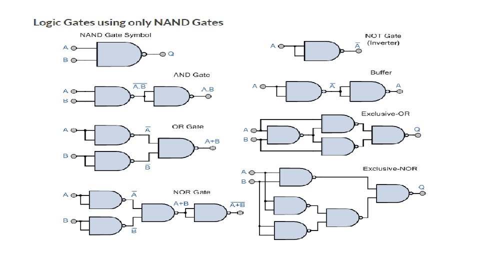

Implementation of OR gate using NAND Gate
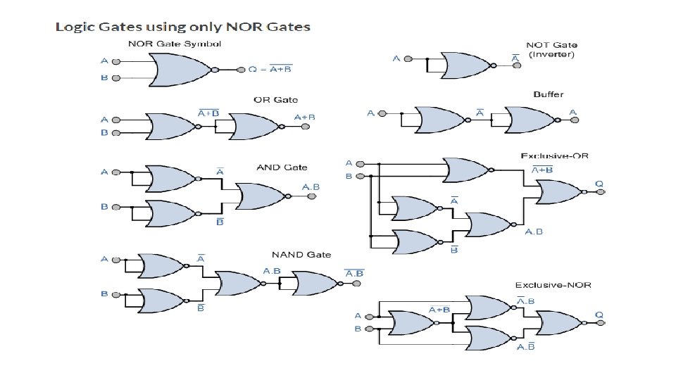

Implementation of AND gate using NOR Gate

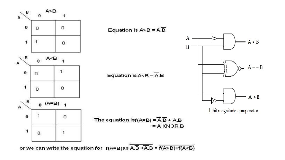
COMPARATORS • Comparator is a combinational logic circuit that compares the magnitudes of two binary quantities(Numbers) to determine which one number has less, equal or greater magnitude. • In other word, a comparator determines the relationship of two binary quantities. • A exclusive - NOR gate can be used as a basic comparator. Magnitude Comparator • Three binary variables are used to indicate the outcome of the comparison as A>B, A<B, or A=B. • The below figure shows the block diagram of a n-bit comparator which compares the two numbers of n-bit length and generates their relation between themselves.

Digital Comparator Types Comparators • 1 -Bit Comparator • 2 -Bit Comparator • 4 -Bit Comparator

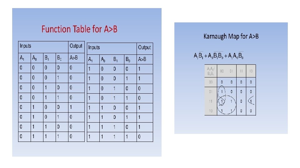
1 bit Magnitude comparator • A comparator used to compare two numbers each of single bit is called single bit comparator. • It consists of two inputs for allowing two single bit numbers and three outputs to generate less than, equal and greater than comparison outputs. • The figure below shows the block diagram of a single bit magnitude comparator. • This comparator compares the two bits and produces one of the 3 outputs as L (A<B), E (A=B) and G (A>B).

There are 1 -bit of two input B and A Truth Table: Block – diagram:

2 - bit Comparator In 2 -bit comparator there are two bits of 2 input and three output:

CIRCUIT DIAGRAM of 2 Bit Comparator
 These are used in the computers and microprocessor devices to")
Applications of Comparators 1) These are used in the computers and microprocessor devices to select a specific input/output device for the storage. 2) 2) These are used in control applications in which the binary numbers representing physical variables such as temperature, position, etc. are compared with a reference value. 3) 3) Process controllers (ON/OFF, self-tune, and manual tune) 4) 4) Servo-motor control ( Electrical plus)

MULTIPLEXER o A MULTIPLEXER is a digital circuit that has multiple inputs and a single output. o The selection of one of the n inputs is done by the select inputs o It has one output selected at a time. o It is also known as DATA SELECTOR. o A multiplexer has N data inputs(multiple) 1 output (single) M select inputs, with 2 M =N
 4 -to-1 (2")
BLOCK DIAGRAM OF MULTIPLEXER : Types: 2 -to-1 (1 select line) 4 -to-1 (2 select lines) 8 -to-1 (3 select lines) 16 -to-1 (4 select lines)
 MULTIPLEXER Here 2: 1 means 2 inputs and 1")
2 -TO-1 (1 SELECT LINES) MULTIPLEXER Here 2: 1 means 2 inputs and 1 output BLOCK DIAGRAM TRUTH TABLE S OUTPUT Y 0 D 0 1 D 1

The logical level applied to the S input determines which AND gate is enabled, so that its data input passes through the OR gate to the output. The output, Y=D 0 S’+D 1 S When S=0, AND gate 1 is enabled and AND gate 2 is disabled. So, Y=DO S=1, AND gate 1 is disabled and AND gate 2 is enabled. So, Y=D 1
 Multiplexer 4: 1 MUX has 4 inputs(D 0, D")
4 -to-1 (2 select lines) Multiplexer 4: 1 MUX has 4 inputs(D 0, D 1, D 2, D 3) & 2 select lines(S 0, S 1) BLOCK DIAGRAM D 0 D 1 D 2 D 3 MUX S 1 S 0 Y TRUTH TABLE S 1 S 0 Y 0 0 D 0 0 1 D 1 1 0 D 2 1 1 D 3

The logical level applied to the S input determines which AND gate is enabled, so that its data input passes through the OR gate to the output. The output, Y=S 1’S 0’D 0+S 1’S 0 D 1+S 1 SO’D 2+S 1 S 0 D 3
 MULTIPLEXER 8: 1 MUX has 8 inputs(D 0, D")
8 -TO-1 (3 SELECT LINES) MULTIPLEXER 8: 1 MUX has 8 inputs(D 0, D 1, D 2, D 3, D 4, D 5, D 6, D 7) & 3 select lines(S 0, S 1, S 2) BLOCK DIAGRAM TRUTH TABLE S 2 S 1 S 0 Out 0 0 0 D 0 0 0 1 D 1 0 D 2 0 1 1 D 3 1 0 0 D 4 1 0 1 D 5 1 1 0 D 6 1 1 1 D 7 9

The logical level applied to the S input determines which AND gate is enabled, so that its data input passes through the OR gate to the output.

Uses of Multiplexers Used in data communications for several computers to communicate over 1 line Used in radio to select one channel from many Used to route data within a computer Used for function generation

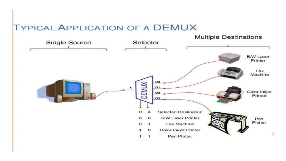
APPLICATION OF MULTIPLEXER: Multiple Sources Selector Single Destination MP 3 Player Docking Station Laptop Sound Card D 1 D 2 MUX D 0 Y D 3 Surround System Digital Satellite Digital Cable TV B A Selected Source 0 0 MP 3 0 1 Laptop 1 0 Satellite 1 1 Cable TV
 Consider an integer ‘m’, which isconstrained")
EXAMPLE OF A COMBINATORIAL CIRCUIT: A MULTIPLEXER (MUX) Consider an integer ‘m’, which isconstrained by the following relation: m = 2 n, where m and n are both integers. A m-to-1 Multiplexer has m Inputs: I 0, I 1, I 2, . . . . I(m-1) one Output: Y n Control inputs: S 0, S 1, S 2, . . . S(n-1) One (or more) Enable input(s) such that Y may be equal to one of the inputs, depending upon the control inputs.

Implementing Digital Functions by using a Multiplexer: In this example to design a 3 variable logical function, we try to use a 4 -to-1 MUX rather than a 8 -to-1 MUX. F(x, y, z)=∑ (m(1, 2, 6, 7) In a canonic form: F = x’. y’. z+ x’. y. z’+x. y’. z’ +x. y. z …… (1) One Possible Solution: Assume that x = S 1 , y = S 0. If F is to be obtained from the output of a 4 -to-1 MUX, F =S’ 1. S’ 0. I 0 + S’ 1. S 0. I 1 + S 1. S’ 0. I 2 + S 1. S 0. I 3 From (1) and (2), I 0 = I 3 =Z I 1 = I 2 =Z’ …. (2)

Implementing Digital Functions by using a Multiplexer:

Implementing Digital Functions by using a Multiplexer:

Implementing Digital Functions by using a Multiplexer:

Implementing Digital Functions by using a Multiplexer:

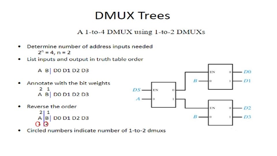
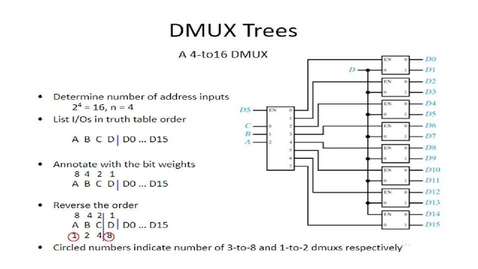
MUX TREES – Implement Higher Order Mux Using Lower Order Mux • A 4 X 1 Mux Can be implemented using three 2 X 1 Mux • By Truth Table we can analyze and find the output expression as: - S 1 S 0 Y 0 0 I 0 0 1 I 1 1 0 I 2 1 1 I 3

16 x 1 Mux using 4 x 1 Mux

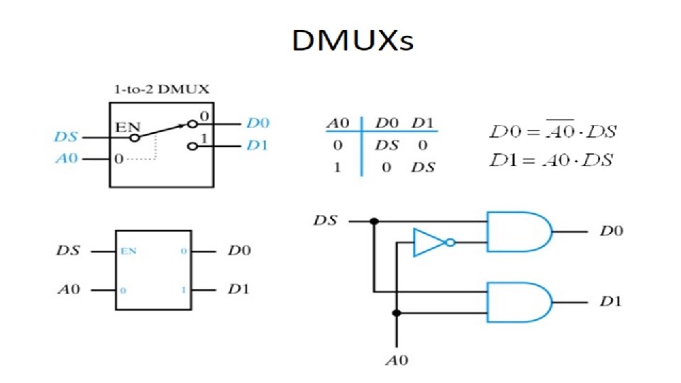
Demultiplexers A demultiplexer has N control inputs 1 data input 2 N outputs A demultiplexer routes (or connects) the data input to the selected output. The value of the control inputs determines the output that is selected. A demultiplexer performs the opposite function of a multiplexer. Types Of Demultiplexer De-multiplexers are classifiedinto four types: 1 -2 demultiplexer (1 select line) 1 -4 demultiplexer (2 select lines) 1 -8 demultiplexer (3 select lines) 1 -16 demultiplexer (4 select lines)
 Out 1 Out 2 Y 0 Y 1 Y")
Demultiplexers (1 TO 4 DEMUX) Out 1 Out 2 Y 0 Y 1 Y 2 Out 3 Y 3 Out 0 Data In Y 0 = A'. B'. I Y 1 = A. B'. I Y 2 = A'. B. I Y 3 = A. B. I S 1 S 0 A B Y 0 Y 1 Y 2 Y 3 0 0 I 0 0 1 0 0 0 I 0 1 1 0 0 0 I

1 -4 DEMULTIPLEXER Truth Table
")
1 -to-8 (3 select lines)
")
1 -TO-16 (4 SELECT LINES)

DECODER • A decoder is a combinational circuit. • A decoder accepts a set of inputs that represents a binary number and activates only that output corresponding to the input number. All other outputs remain inactive. • The block diagram of decoder with ‘N’ inputs and ‘M’ outputs is shown. • There are 2 N possible input combinations, for each of these input combination only one output will be HIGH (active) all other outputs are LOW • Some decoder have one or more ENABLE (E) inputs that are used to control the operation of decoder.

BLOCK DIAGRAM OF DECODER A 0 A 1 A 2 . . DECODER . . AN-1 B 0 B 1 B 2 BM-1 N- Inputs M- Outputs Only one output is High for each input

2 to 4 Line Decoder: Block diagram of 2 to 4 decoder is shown below A and B are the inputs. ( No. of inputs =2) No. of possible input combinations: 22=4 No. of Outputs : 22=4, they are indicated by D 0, D 1, D 2 and D 3 From the Truth Table it is clear that each output is “ 1” for only specific combination of inputs. TRUTH TABLE A B Inputs 2 X 4 Decoder D 0 INPUTS D 1 A B D 0 D 1 D 2 D 3 0 0 1 0 0 1 0 0 0 1 Outputs OUTPUTS

BOOLEAN EXPRESSION: From Truth Table D 0 A B D 1 A B D 2 A B LOGIC DIAGRAM: D 3 AB A A B B D 0 A B D 1 A B D 2 A B D 3 A B

3 to 8 Line Decoder: Block diagram of 3 to 8 decoder is shown below A , B and C are the inputs. ( No. of inputs =3) No. of possible input combinations: 23=8 No. of Outputs : 23=8, they are indicated by D 0 to D 7 From the Truth Table it is clear that each output is “ 1” for only specific combination of inputs. A B C Inputs 3 X 8 Decoder . D 0. . D 7 Outputs

TRUTH TABLE FOR 3 X 8 DECODER: INPUTS OUTPUTS A B C D 0 D 1 D 2 D 3 D 4 D 5 D 6 D 7 0 0 0 1 0 0 0 0 D 0 A B C 0 0 1 0 0 0 D 1 A B C 0 1 0 0 0 0 0 D 2 A B C 0 1 1 0 0 0 0 D 3 A B C 1 0 0 0 D 4 A B C 1 0 0 0 1 0 0 D 5 A B C 1 1 0 0 0 0 1 0 D 6 A B C 1 1 1 0 0 0 0 1 D 7 A B C

LOGIC DIAGRAM OF 3 X 8 DECODER: INPUTS B A A C B C D 0 A B C D 1 A B C D 2 A B C D 3 A B C D 4 A B C D 5 A B C D 6 A B C D 7 A B C OUTPUTS

EXPANSION OF DECODERS: The number of lower order Decoder for implementing higher order Decoder can be find as No. of lower order required = m 2/m 1 Where, m 1=No. of Outputs of lower order Decoder m 2=No. of Outputs of higher order Decoder 3 x 8 Decoder From 2 x 4 Decoder:

Example: Implement the following multiple output function using a suitable Decoder. f 1(A, B, C) = ∑m(0, 4, 7)+ d(2, 3) f 2 (A, B, C) =∑m (1, 5, 6) f 3 (A, B, C) =∑m (0, 2, 4, 6) Solution: f 1 consists of don’t care conditions. So we consider them to be logic 1. A 2 B 3 C 3 x 8 Decoder INPUTS 0 1 f 1(A, B, C) f 2 (A, B, C) 4 5 6 7 f 3 (A, B, C)
=∑m(1,")
EXAMPLE: Implement the following Boolean function using suitable Decoder. f 1 (x, y, z)=∑m(1, 5, 7) f 2 (x, y, z)=∑m(0, 3) f 3 (x, y, z)=∑m(2, 4, 5) Solution: 0 1 Y Z E 2 3 X 8 Decoder INPUTS X f 1 (x, y, z) 3 f 2 (x, y, z) 4 5 6 7 f 3 (x, y, z)

ENCODER A 0 B 2 AM-1 Encoder - - - - A 2 - - - - A 1 B 0 B 1 BN-1 ‘N’ Outputs An Encoder is a combinational logic circuit. It performs the inverse operation of Decoder. The opposite process of decoding is known as Encoding. An Encoder converts an active input signal into a coded output signal. Block diagram of Encoder is shown in below. It has ‘M’ inputs and ‘N’ outputs. An Encoder has ‘M’ input lines, only one of which is activated at a given time, and produces an N-bit output code, depending on which input is activated. ‘M’ Inputs • • •

• Encoders are used to translate the rotary or linear motion into a digital signal. • The difference between Decoder and Encoder is that Decoder has Binary Code as an input while Encoder has Binary Code as an output. • Encoder is an Electronics device that converts the analog signal to digital signal such as BCD Code. • Types of Encoders i. Priority Encoder ii. Decimal to BCD Encoder iii. Octal to Binary Encoder iv. Hexadecimal to Binary Encoder

DECIMAL TO BCD ENCODER: • It has ten inputs corresponding to ten decimal digits (from 0 to 9) and four outputs (A, B, C, D) representing the BCD 0 A 1 9 INPUTS - - - - - 2 B ENCODER C D OUTPUTS

Truth table: INPUTS BCD OUTPUTS 0 1 2 3 4 5 6 7 8 9 A B C D 1 0 0 0 0 1 0 0 0 0 0 1 0 0 0 0 0 0 1 0 0 0 0 0 1 0 0 1 1 0 0 0 0 1 1 1 0 0 0 0 0 0 0 1 1 0 0 1

• From Truth Table it is clear that the output A is HIGH when input is 8 OR 9 is HIGH Therefore A=8+9 • The output B is HIGH when 4 OR 5 OR 6 OR 7 is HIGH Therefore B=4+5+6+7 • The output C is HIGH when 2 OR 3 OR 6 OR 7 is HIGH Therefore C=2+3+6+7 • Similarly D=1+3+5+7+9 Logic Diagram is shown

OCTAL TO BINARY ENCODER: • • Block Diagram of Octal to Binary Encoder is shown It has eight inputs and three outputs. Only one input has one value at any given time. Each input corresponds to each octal digit and output generates corresponding Binary Code. D 0 D 1 D 2 D 3 ENCODER D 4 D 5 D 6 D 7 INPUT X Y Z OUTPUT

TRUTH TABLE: INPUT OUTPUT D 0 D 1 D 2 D 3 D 4 D 5 D 6 D 7 X Y Z 1 0 0 0 1 0 0 0 0 0 0 1 0 0 0 1 1 0 0 0 0 0 1 0 0 0 1 0 1 1 0 0 0 0 1 1

From Truth table: X D 7 D 4 Y Z D 2 D 5 D 1 D 3 D 6 D 5 D 7 • It is assume that only one input is HIGH at any given time. If two outputs are HIGH then undefined output will produced. For example D 3 and D 6 are HIGH, then output of Encoder will be 111. This output neither equivalent code corresponding to D 3 nor to D 6. • To overcome this problem, priorities should be assigned to each input. • Form the truth table it is clear that the output X becomes 1 if any of the digit D 4 or D 5 or D 6 or D 7 is 1. • D 0 is considered as don’t care because it is not shown in expression. • If inputs are zero then output will be zero. Similarly if D 0 is one, the output will be zero.

PRIORITY ENCODER: • As the name indicates, the priority is given to inputs line. • If two or more input lines are high at the same time i. e 1 at the same time, then the input line with high priority shall be considered. • Block diagram and Truth table of Priority Encoder are shownbelow Highest Priority Input D 3 TRUTH TABLE: D 2 D 1 D 0 INPUTS Y 1 Priority Encoder Y 0 Lowest Priority Output Input Block Diagram of Priority Encoder OUTPUTS V D 3 D 2 D 1 D 0 Y 1 Y 0 0 0 x x 0 0 1 x 0 1 1 0 1 x x 1 0 1 1 x x x 1 1 1

• • There are four inputs D 0, D 1, D 2, D 3 and two outputs Y 1 and Y 2. D 3 has highest priority and D 0 is at lowest priority. If D 3=1 irrespective of other inputs then output Y 1 Y 0=11. D 3 is at highest priority so other inputs are considered as don’t care. K-map for Y 1 and Y 0 D 1 D 0 D 3 D 2 00 01 11 10 00 X 0 00 01 1 1 11 1 10 1 1 1 D 3 D 2 Y 1 D 2 D 3 00 01 11 10 X 0 1 1 01 0 0 1 11 1 1 10 1 1 Y 0 D 3 D 2 D 1

LOGIC DIAGRAM OF PRIORITY ENCODER: Y 1 D 2 D 3 Y 0 D 3 D 2 D 1 D 3 D 2 D 1 D 0 Y 1 Y 0

Adder � An adder is a digital logic circuit in electronics that implements addition of numbers. � In many computers and other kinds of processors, adders are used not only in • the arithmetic logic units, but also in other parts of the processor, where they are used to calculate addresses, increment and decrement operators, and similar operations. Adders are classified into two types: 1)half adder. 2)full adder. Let us first take a look at the addition of single bits. � 0+0 = 0 � 0+1 = 1 � 1+0 = 1 � 1+1 =10 (i. e. 1+1=0 with carry = 1)

Half Adder: is a combinational circuit that performs the addition of two bits, this circuit needs two binary inputs and two binary outputs. The simplified Boolean function from the truth table: X XY Y X S C Implementation of Half Adder using equation (1) Y S C Implementation of Half Adder using equation (2)

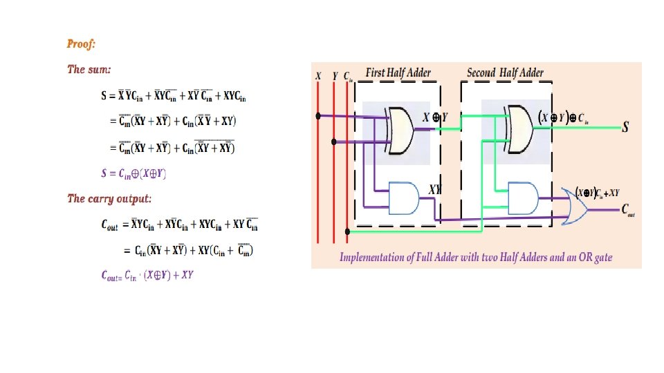
Full Adder • Full Adder is a combinational circuit that performs the addition of three bits (two significant bits and previous carry). • It consists of three inputs and two outputs, two inputs are the bits to be added, the third input represents the carry form the previous position. • The full adder is usually a component in a cascade of adders, which add 8, 16, etc, binary numbers. The output is equal to 1 when only one input is equal to 1 or when all three inputs are equal to 1. The output has a carry 1 if two or three inputs are equal to 1. The Karnaugh maps and the simplified expression are shown in the following figures:

The logic diagrams for the full adder implemented in sum-of-products form are the following: It can also be implemented using two half adders and one OR gate (using XOR gates).

BINARY SUBTRACTOR RULES FOR BINARY SUBTRACTION 0 - 0 = 0 0 - 1 = 1 1 - 0 =1 1 – 1=0 with borrow 1 NOTE: In the second case (0 – 1) it is necessary to borrow a 1. TYPES OF BINARY SUBTRACTOR • • Half Subtractor Full Subtractor

Half Subtractor: • It is a combinational circuit with two inputs and two outputs ( difference and borrow) • Two inputs are A (minuend), B (subtrahend) and two outputs are D (difference) and Bo (borrow out). • It is used to perform subtraction of two bits. TRUTH TABLE OF HALF-SUBTRACTOR INPUTS Minuend OUTPUTS Subtrahend (B) Difference Borrow (Bo) (D) (A) 0 0 0 1 1 0 0 K-Map for difference (D) B 0 0 0 1 1 0 A AB B 0 A 0 0 1 0 AB LOGIC DIAGRAM A B D Bo 1 1 AB 0 K-Map for Borrow Output (Bo)

FULL SUBTRACTOR: • Full subtractor is a combinational circuit. • It performs subtraction involving three bits (i) minuend bit (ii) subtrahend bit (ii) borrow from the previous stage. • It has three inputs (i) X (minuend) (ii) Y (subtrahend) (iii) Bin from the previous stage. • It has two outputs D (difference) and Borrow out Bout. LOGIC SYMBOL: X Y Bin D FULL SUBTRACTOR Bout
 TRUTH TABLE: INPUTS OUTPUTS X Y Bin D Bout")
K-Map For Difference Output (D) TRUTH TABLE: INPUTS OUTPUTS X Y Bin D Bout 0 0 0 0 1 1 1 0 1 1 0 0 1 0 1 0 0 1 1 1 0 0 0 1 1 YBin 00 X 0 0 01 1 0 1 0 1 11 10 D XY Bin XYBin K-Maps For Borrow Output (Bout) X YBin 00 01 11 10 0 0 1 1 0 0 1 0 Bout XY X Bin YBin
B i n D ( X")
D XY Bin XYBin D ( X Y )B i n D ( X Y )B i n D X Y B i n • Equation for a borrow output is resembles the carry output of full adder except that one of the input is complemented. • Equation for D is same as the sum of output for a full adder. • It is possible to convert a full adder into a full subtractor by complementing that input before to its applied to the input of gates which form the borrow output.

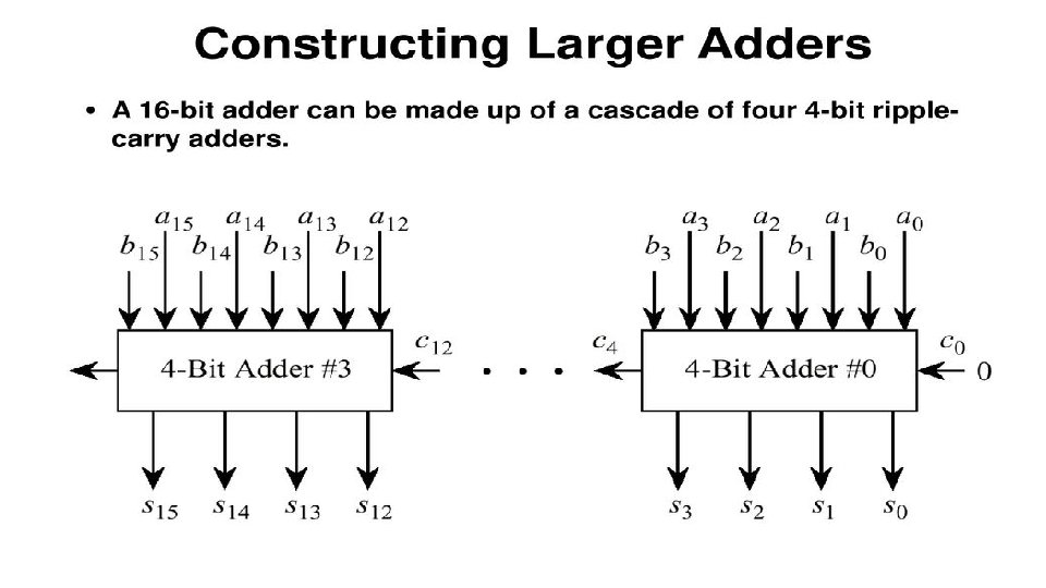
Parallel Adder • A circuit , consisting of n full adders , that will add n-bit binary numbers. • The output consists of n sum bits and a carry bit. • CO of one full adder is connected to CI of the next full adder. Structure Of Parallel Adder • Parallel adder nothing but a cascade of several full adders. • The number of full adders used will depend on the number of bits in the binary digits which require to be added. Different Types Of Binary Adder • ONE BIT PARALLEL ADDER • TWO BIT PARALLER ADDER • FOUR BIT PARALLER ADDER

BLOCK DIAGRAM OF ONE and TWO BIT PARALLEL ADDER

BLOCK DIAGRAM OF n BIT PARALLEL ADDER When an n-bit binary number is added to another, each column generates a sum and a 1 or 0 carry to the next higher order column. (When n=4)

For an example: A = 1011 B = 0011 S = 1110 Demonstration: subscript 4 3 2 1 Input carry 0 1 1 0 Ci Augend 1 0 1 1 Ai Addend 0 0 1 1 Bi Sum 1 1 1 0 Si Output carry 0 0 1 1 Ci+1

Procedure The bits are added with full-adder. Starting from the least significant position to form the sum and carry. The input carry CI 1 in the least significant position must be zero. The value of CIi+1 in a given significant position is the output carry CO of the full adder. This value is transferred into the input carry CI of the full-adder that adds the bits one higher significant position to left. The sum bits are thus generated starting from the rightmost position and are available as soon as the corresponding previous carry bit is generated.

Ripple Carry Subtractor: - Subtraction is done using 2’s Complement method
 is at a low logic,")
Ripple Carry Adder-Subtractor • When the mode input (M) is at a low logic, i. e. '0', the circuit act as an adder and when the mode input is at a high logic, i. e. '1', the circuit act as a subtractor. • The exclusive-OR gate connected in series receives input M and one of the inputs B. • When M is at a low logic, we have B⊕ 0 = B. The full-adders receive the value of B, the input carry is 0, and the circuit performs A plus B. • When M is at a high logic, we have B⊕ 1 = B' and C 0 = 1. The B inputs are complemented, and a 1 is added through the input carry. The circuit performs the operation A plus the 2's complement of B. M

Serial Adder • The serial adder is a binary adder that is capable of forming sum and carry outputs for addend augend words of greater than one bit in length. • If speed is not of great importance, a cost-effective option is to use a serial adder • Serial adder: bits are added a pair at a time (in one clock cycle) A=an-1 an-2…a 0, B=bn-1 bn-2…b 0

al. Comparison Adder between parallel. Parallel & Serial and serial adder • • • Serial Parallel Faster. • Slower It uses registers with parallel • It uses shift registers. load capacity. • It requires one full adder circuit. Number of full adder circuit is equal • It is sequential circuit. to number of bits in binary adder. • Time required for addition depends on It is a combinational circuit. number of bits. Time required does not depend on the number of bits

BCD ADDER • Also Known as 8421 digit. A 4 -bit binary adder. • Adds two 4 -bit digits having a BCD. Resulting format 4 -bit output digit. • Sum exceeding decimal value of 9, a carry’s generated. • The BCD Number is Valid for sum less than 9 as the sum exceeds then a correction factor, 6 is added to the sum (12) 10 1100 00010010 Conversion and Coding (using BCD code for each digit)

� Why add 6 to the result? Sum of two BCD digits exceeding 9. A carry is generated. Converting the invalid digit into valid digit. Carry generated by adding 6 to the invalid BCD digit’s passed on to the next BCD digit.

Designing BCD Adder

Example 1

Example 2

Barrel Shifter • In Binary Operation, shifting is a bitwise operation that shifts the operand I to n-1 places to the right or left • N-bit shifter is a device which shifts the input data to n-1 places to the left or right

Shift Logic • Left Shift • Right Shift • N-bit shift = original data • K-bit right shift = n-k bit left shift

Crossbar Switch • In telecommunications, a crossbar switch (also known as cross-point switch, or matrix switch) is a switch connecting multiple inputs to multiple outputs in a matrix manner.

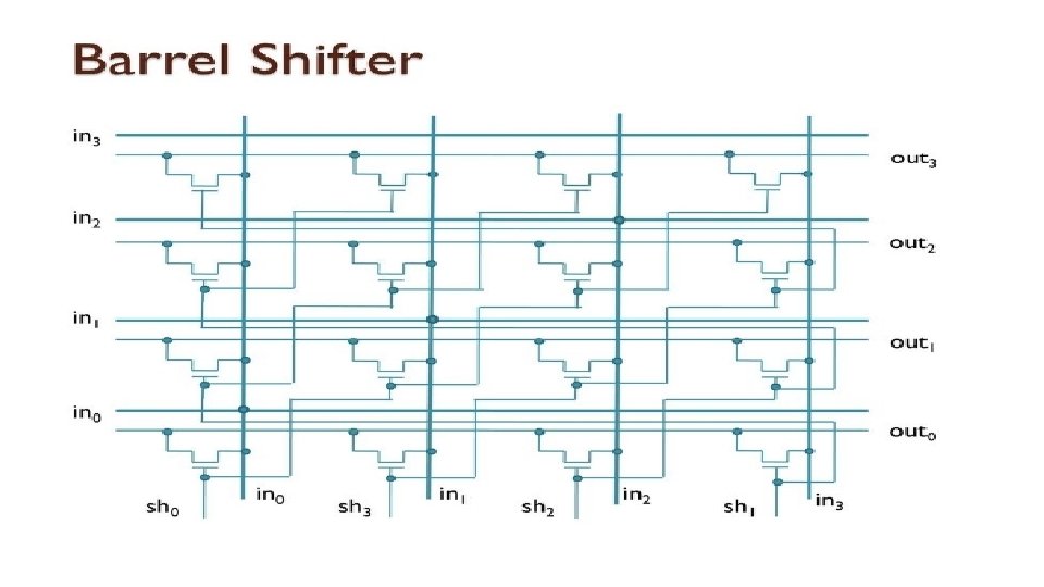
Barrel Shifter • A barrel shifter is a digital circuit that can shift a data word by a specified number of bits without the use of any sequential logic, only pure combinational logic. • One way to implement it is as a sequence of multiplexers where the output of one multiplexer is connected to the input of the next multiplexer in a way that depends on the shift distance. • A barrel shifter is often used to shift and rotate n-bits in modern microprocessors, typically within a single clock cycle. • For example, take a four-bit barrel shifter, with inputs A, B, C and D. The shifter can cycle the order of the bits ABCD as DABC, CDAB, or BCDA; in this case, no bits are lost. That is, it can shift all of the outputs up to three positions to the right (and thus make any cyclic combination of A, B, C and D). • The barrel shifter has a variety of applications, including being a useful component in microprocessors (alongside the ALU).

Shifting of Bits
 (If S 1")
Barrel Shifter using Multiplexer (If S 1 S 0 = 00) (If S 1 S 0 = 01) (If S 1 S 0 = 10) (If S 1 S 0 = 11) D 0 D 3 D 2 D 1 D 0 D 3 D 2 D 1 D 0
 • ALU is a purely combinational device: It has no")
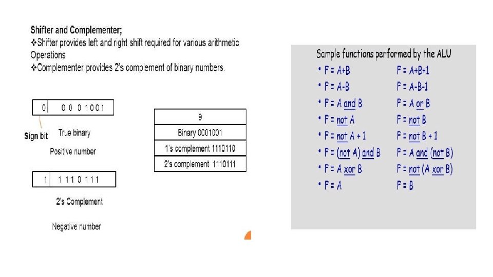
Arithmetic Logic Unit (ALU) • ALU is a purely combinational device: It has no memory or internal storage • It has two input vectors These may be called as A and B vector or the R and S vector The inputs are as wide as registers/ system bus (i. e. 16, 32 bits) • It has one output vector Usually denoted as F

ALU Block Diagram

Example - Performing a Arithmetic operation

Multiplexed Display • Multiplexing is a technique used to connect devices – typically LEDs (for displays) or buttons (for keyboards) – in a matrix of addressable rows and columns. • The advantage is simplification of hardware due to the reduced number of pins required. Multiplexed displays using seven-segment LEDs remain popular due to low cost and high brightness.

Operation • A practical circuit uses transistorised switches. • Each row is switched on in sequence (S 1, then S 2 and then S 3) and the corresponding switches S 4, 5, 6 and 7 closed in synch to switch on the desired LEDs. • To fool the eye into seeing a continuous display the sequencing is typically done at more than 50 times per second. • In the example (Previous Slide), only seven lines are required to switch twelve LEDs. • The pin-count saving increases with larger displays as the pin-count (for a square matrix) is the square root of the number of LEDs. This reduces the pins required on the controller, reducing cost and circuit board complexity. • Since the LEDs are now on for only a fraction of the time it is necessary to pulse them with higher current.

Seven Segment Display – It has also same arrangement of LED Two Types – 1) Common Cathode 2) Common Anode

Driving a Segment Display using Switches � � The segments of a common anode display can be illuminated using the switches. In this a LOW condition is required to activate the LED segments on this common anode display. eg: illuminate the decimal number “ 4” on the display, the switches b, c, f and g would be closed to light the corresponding LED segments.

Driving a Segment Display using 4511 IC � � 7 -segment Displays are usually driven by a special type of integrated circuit (IC) like CMOS 4511. This 7 -segment display driver is able to illuminate both common anode or common cathode displays. This BCD-to-7 segment driver takes a four-bit BCD input and has outputs that will pass current through the segments to display the decimal digit.

Application of Multiplexed Display As Seven segment display provides a convenient way to display decimal numbers in digital form, it is helpful in general purpose devices and reduces the complexity of data delivered. It is used in many devices of our day to day life, like in traffic signals, watches, cd/dvd players etc.

THANKS
- Slides: 126