DIGITAL SIGNAL PROCESSORS Von Neumann Architecture Computers to


")


.")


 filter use")

- Slides: 36
DIGITAL SIGNAL PROCESSORS
Von Neumann Architecture • Computers to be programmed by codes residing in memory. • Single Memory to store data and program. • Single Bus to transport data and program b/w CPU and memory/pheripherals.
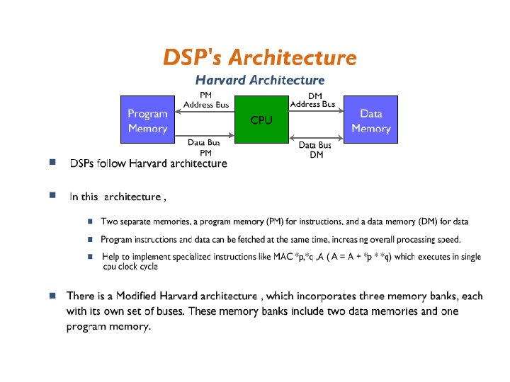
Harvard Architecture • Separate memory for data and program • Separate program bus for transferring opcode and immediate operands b/w CPU and program memory. • Separate data memory bus to transfer data b/w data memory and CPU.
Modified Harvard Architecture • • Multiport memories (one PM, 3 DM and 4 AB) CPU can access multiple data simultaneously Increased speed Dedicated h/w for signal processing applications.
What Constitutes a Good DSP?
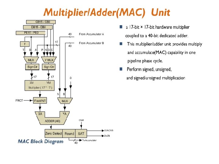
DSP Requires Multiply and Accumulate
Multiple Buses
Internal Memory for Fast Access
• Most of the early processors execute instructions sequentially. • After the execution of first instruction the next one starts. • To improve the efficiency, advanced microprocessors and digital signal processors use an approach called pipelining.
Instruction Pipeline for Fast Execution Instruction is broken into smaller tasks that can be executed in parallel
Parallel Processing of Instructions
Less Cycles per Instruction Less Power Consumption
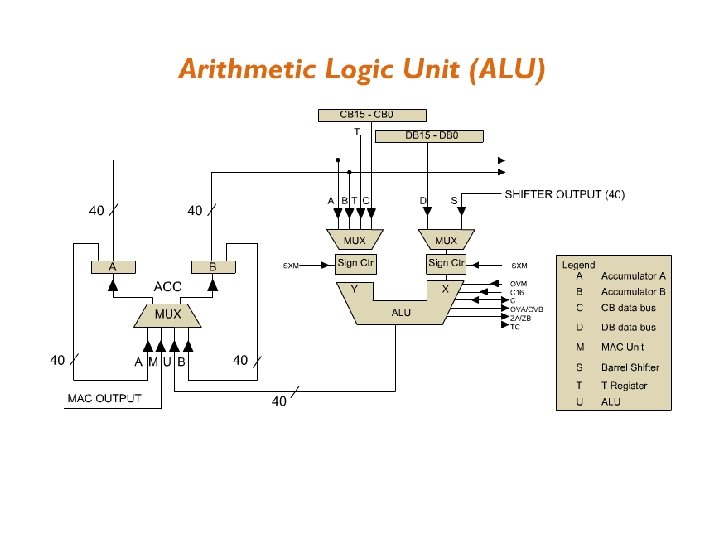
DSP Architecture
Internal Memory Organization • Program, data and I/O spaces. • RAM and ROM(boot loader). • Types of RAM (DARAM , SARAM and two-way shared RAM). • DARAM AND SARAM configured as DM or PM/DM.
DARAM • Composed of several blocks and can be accessed twice per machine cycle. • Read and write operation can be done in the same cycle. • Mapped in data space or program space.
SARAM and two-way shared RAM • Accessed for once per machine cycle for either read or write. • Shared memory is write-protected and only DMA can write to the SM. • RAM efficiently used for executing identical programs( 50% memory space is reduced).
Addressing Modes
Addressing Modes • Immediate addressing • Direct addressing • Indirect addressing by register – Support for circular indirect addressing • Access to Memory Mapped Registers MMRs • Dedicated register addressing. • Circular addressing
Immediate Addressing Mode # • Instruction contains the value of the operand. Value is preceded by #. ADD #4, A • Example: – Add the value 4 to the content of accumulator A. • Useful for initializations. • Long (16 bits) or short values: – For long values: instruction uses 2 words.
Immediate Addressing Mode # • 16 bit value – 2 words, 2 cycles – Initialization of ARi for example Example: STM #1234 h, AR 2 Load AR 2 with the value 1234 h. • Short value – 3, 5, 8, 9 bits constant – 1 word, 1 cycle – To initialize short length registers or bit fields: • DP, ASM … – Not always available Example: LD #6, DP Load DP with the value 6.
Direct Addressing Mode @ • Direct addressing = random access from a specified base address. – The instruction contains an offset relative to the base address. • The base address can be the beginning of a data memory page or the stack pointer. – The data memory is virtually divided in 512 pages of 128 words (512 x 128 = 216). • Data Page DP relative direct address – CPL bit (Com. Piler Mode bit) = 0 in ST 1 • Stack Pointer SP relative direct address – CPL bit = 1 in ST 1
Data memory pages
MMR Memory Mapped Registers Addressing • MMRs are in page 0 of data memory. • They can be accessed by some specific MMR instructions allowing simple access to page 0. • In these cases DP, SP and CPL are ignored • It operates like direct addressing except that upper 9 bits of the address that is accessed are assumed zeros.
Indirect Addressing Mode *ARi • Compatible with pointers in C. • 8 ARi Auxiliary Registers to store the addresses of the operands. They are used as pointers. • 2 ARAU = Auxiliary Registers Arithmetic Units to realize operations on the addresses stored in the ARi. • Contents of AR by ARP can manually altered by SBRK and ADRK. • Very efficient for DSP operations.
Dedicated Register Addressing • Similar long immediate addressing mode except the address comes from the special purpose memory mapped registers in the CPU • Block Move Address Register(BMAR) and the dynamic bit manipulation register(DBMR).
Circular Addressing • Algorithms such as convolution, correlation and finite impulse response(FIR) filter use circular buffers operating via Ars. • CBSR 1 -Circular buffer 1 start register • CBSR 2 • CBER 1 -End register 1 • CBER 2, CBCR-Control Register(Enables/Disables) • To define circular buffer start & end addresses are loaded and a value b/w start and end register is loaded into AR.
THANK YOU