Digital micromirror devicebased adaptive optics approach for enhanced
Digital micromirror device-based adaptive optics approach for enhanced micro-machining fidelity D. J. Heath 1, B. Mills 1, J. A. Grant-Jacob 1, M. Feinaeugle 3, V. Goriainov 2, R. Oreffo 2, R. W. Eason 1 1 Optoelectronics Research Centre, University of Southampton, UK 2 Institute of Developmental Sciences, University of Southampton, UK 3 Department of Mechanical Engineering, University of Twente, The Netherlands
Outline • Past work and challenges in DMD projection-based laser manufacturing • DMD mask shifting • Taking advantage of limited bandwidth • Custom substrates, including cell growth assays • Conclusions 2

DMD-based laser manufacturing • Using 800 nm wavelength, 150 femtosecond laser pulses • Spatial intensity profile of each laser pulse is modified by the DMD, and then imaged on to the sample l ut inp lses pu r e as sp a las tially er pu shap lse s ed sample is translated foc ob ussin jec tiv g e 4 sample movement direction array of mirrors, showing the pattern (the DMD)
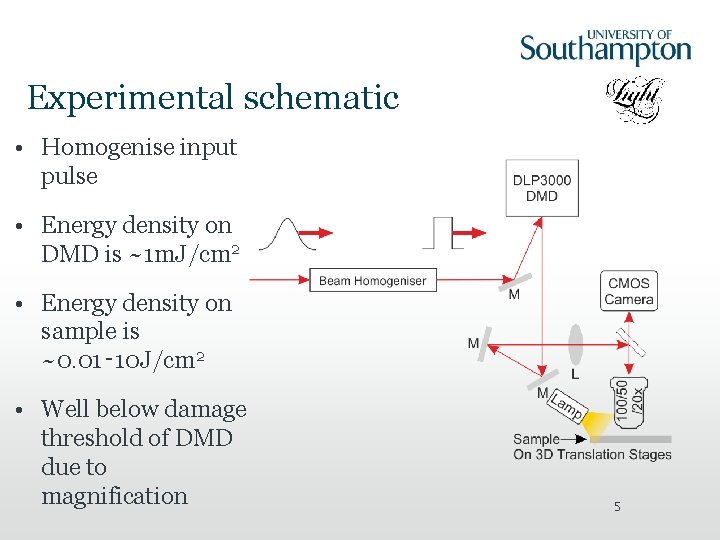
Experimental schematic • Homogenise input pulse • Energy density on DMD is ~1 m. J/cm 2 • Energy density on sample is ~0. 01‑ 10 J/cm 2 • Well below damage threshold of DMD due to magnification 5

DMD-based laser manufacturing • Almost any material • Routinely produce ~1 cm 2 samples • ~2µm resolution each exposure 10µm 50µm 6
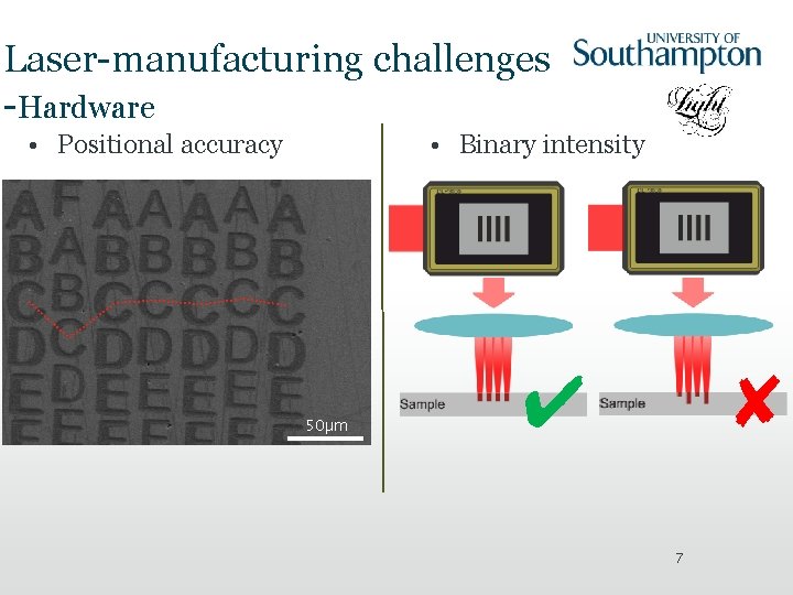
Laser-manufacturing challenges -Hardware • Positional accuracy • Binary intensity 50µm ✔ ✘ 7
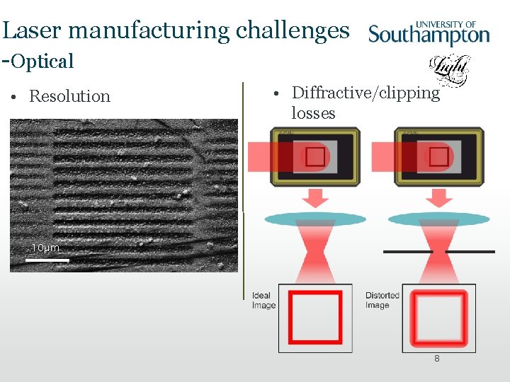
Laser manufacturing challenges -Optical • Resolution • Diffractive/clipping losses 10µm 8
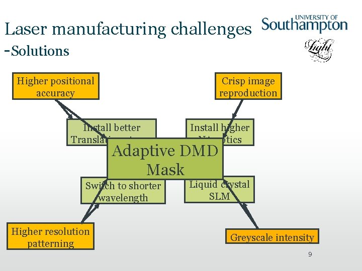
Laser manufacturing challenges -Solutions Crisp image reproduction Higher positional accuracy Install better Translation stages Install higher NA optics Adaptive DMD Mask Switch to shorter wavelength Higher resolution patterning Liquid crystal SLM Greyscale intensity 9
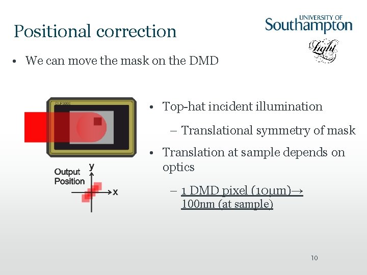
Positional correction • We can move the mask on the DMD • Top-hat incident illumination – Translational symmetry of mask • Translation at sample depends on optics – 1 DMD pixel (10µm)→ 100 nm (at sample) 10
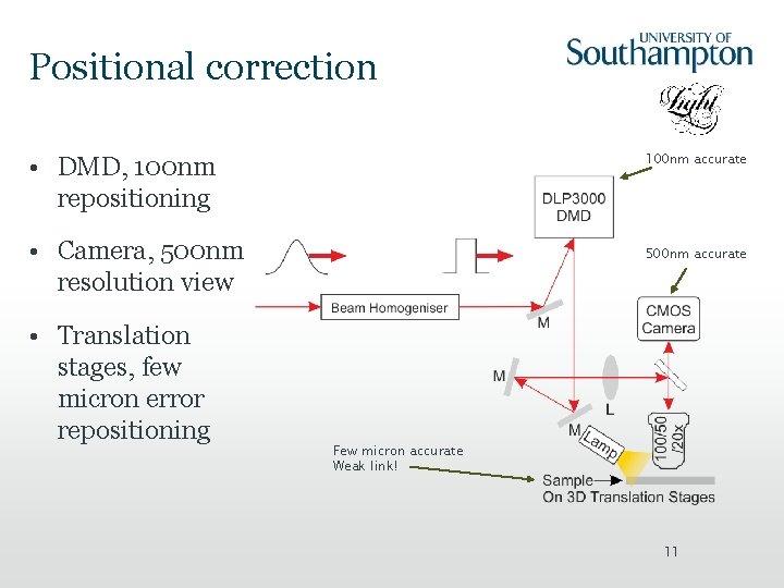
Positional correction 100 nm accurate • DMD, 100 nm repositioning • Camera, 500 nm resolution view • Translation stages, few micron error repositioning 500 nm accurate Few micron accurate Weak link! 11
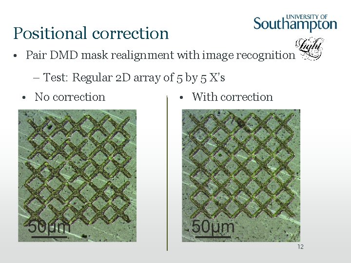
Positional correction • Pair DMD mask realignment with image recognition – Test: Regular 2 D array of 5 by 5 X’s • No correction • With correction 12
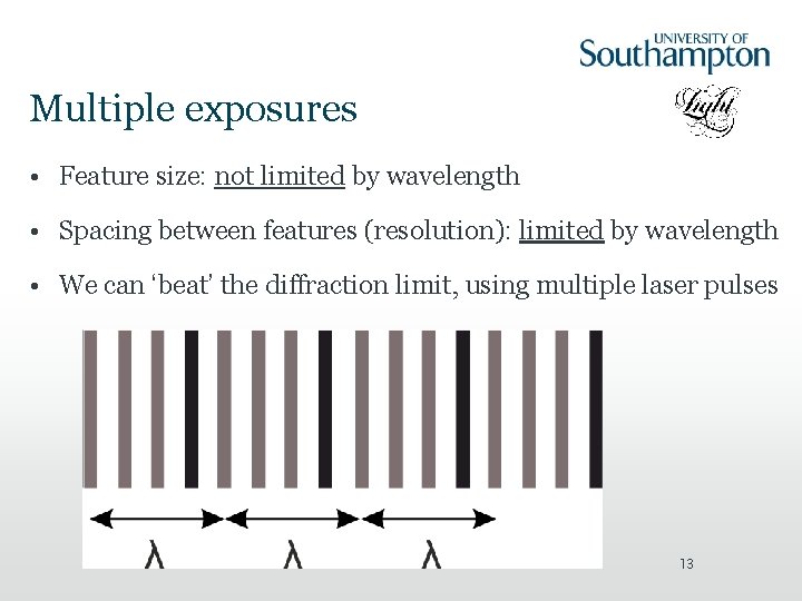
Multiple exposures • Feature size: not limited by wavelength • Spacing between features (resolution): limited by wavelength • We can ‘beat’ the diffraction limit, using multiple laser pulses 13
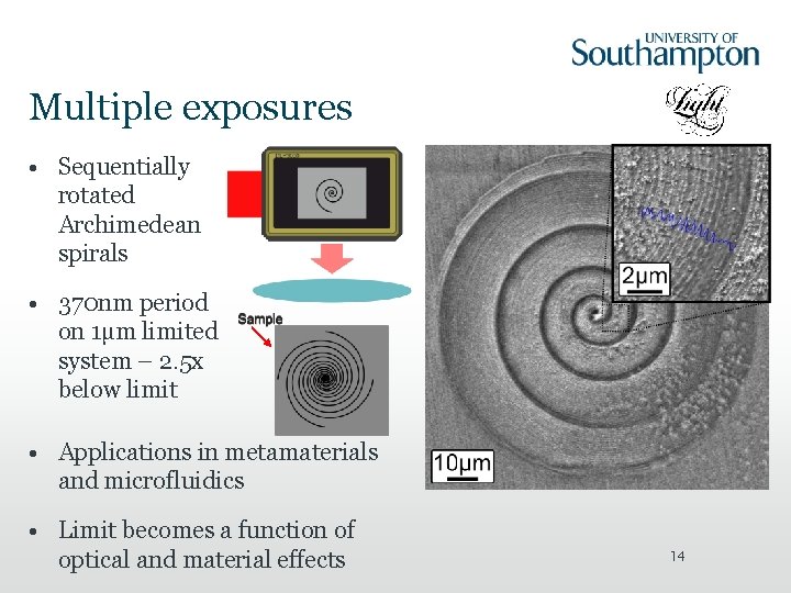
Multiple exposures • Sequentially rotated Archimedean spirals • 370 nm period on 1µm limited system – 2. 5 x below limit • Applications in metamaterials and microfluidics • Limit becomes a function of optical and material effects 14
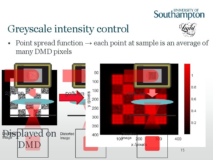
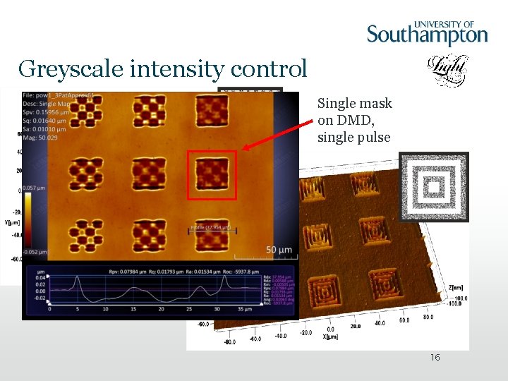
Greyscale intensity control • Point spread function → each point at sample is an average of many DMD pixels 25% on Displayed on DMD 50% on 75% on 15
Greyscale intensity control Single mask on DMD, single pulse 16
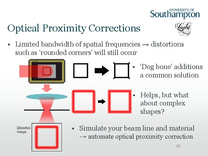
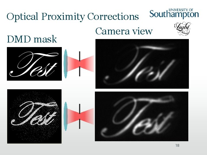
Optical Proximity Corrections • Limited bandwidth of spatial frequencies → distortions such as ‘rounded corners’ will still occur • ‘Dog bone’ additions a common solution • Helps, but what about complex shapes? • Simulate your beam line and material → automate optical proximity correction 17
Optical Proximity Corrections Camera view DMD mask 18
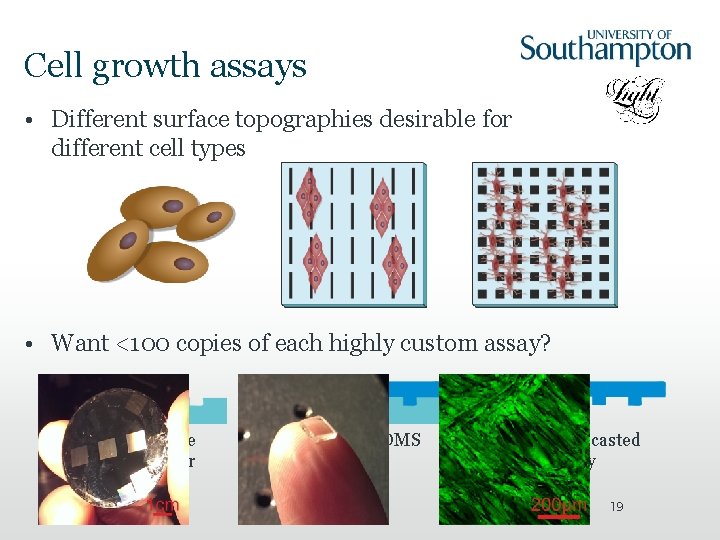
Cell growth assays • Different surface topographies desirable for different cell types • Want <100 copies of each highly custom assay? Laser-machine custom master Drop-cast PDMS Peel away casted assay 19
Conclusions • DMD mask translation → positional correction and subdiffraction limit features • Averaged pixel contributions → short pulse greyscale intensity • Single-pixel control → DMD optical proximity corrections • DMD adaptive mask techniques → solving common laser machining problems 20 This work was supported under EPSRC (grant number EP/L 022230/1)
- Slides: 19