Digital Logic with Molecular Reactions Department of Electrical

- Slides: 22

Digital Logic with Molecular Reactions Department of Electrical and Computer Engineering University of Minnesota Presenter: Chi-Yun Cheng

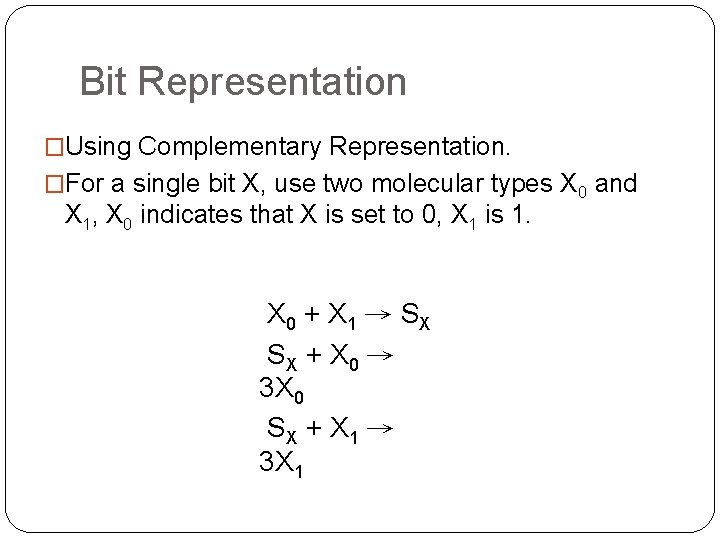
Bit Representation �Using Complementary Representation. �For a single bit X, use two molecular types X 0 and X 1, X 0 indicates that X is set to 0, X 1 is 1. X 0 + X 1 → SX SX + X 0 → 3 X 0 SX + X 1 → 3 X 1

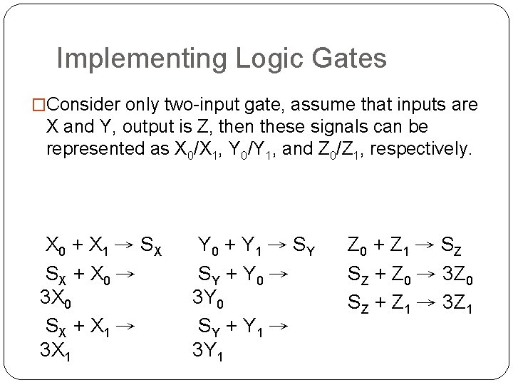
Implementing Logic Gates �Consider only two-input gate, assume that inputs are X and Y, output is Z, then these signals can be represented as X 0/X 1, Y 0/Y 1, and Z 0/Z 1, respectively. X 0 + X 1 → SX SX + X 0 → 3 X 0 SX + X 1 → 3 X 1 Y 0 + Y 1 → SY SY + Y 0 → 3 Y 0 SY + Y 1 → 3 Y 1 Z 0 + Z 1 → SZ SZ + Z 0 → 3 Z 0 SZ + Z 1 → 3 Z 1

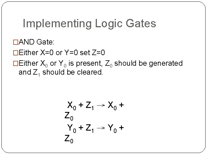
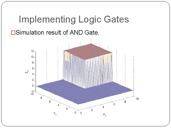
Implementing Logic Gates �AND Gate: �Either X=0 or Y=0 set Z=0 �Either X 0 or Y 0 is present, Z 0 should be generated and Z 1 should be cleared. X 0 + Z 1 → X 0 + Z 0 Y 0 + Z 1 → Y 0 + Z 0

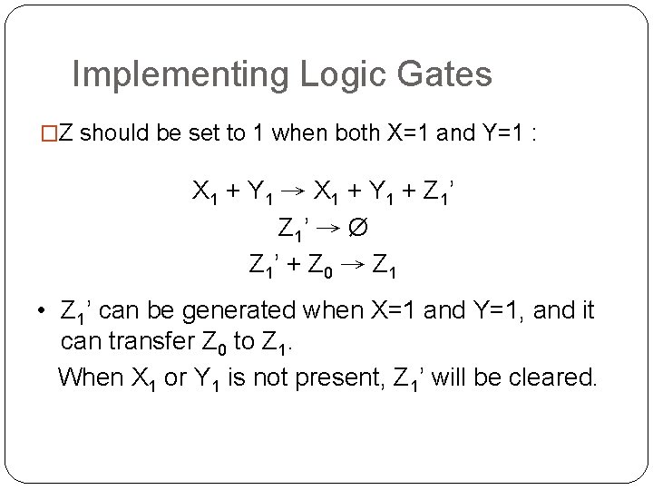
Implementing Logic Gates �Z should be set to 1 when both X=1 and Y=1 : X 1 + Y 1 → X 1 + Y 1 + Z 1’ → Ø Z 1’ + Z 0 → Z 1 • Z 1’ can be generated when X=1 and Y=1, and it can transfer Z 0 to Z 1. When X 1 or Y 1 is not present, Z 1’ will be cleared.

Implementing Logic Gates �Simulation result of AND Gate.

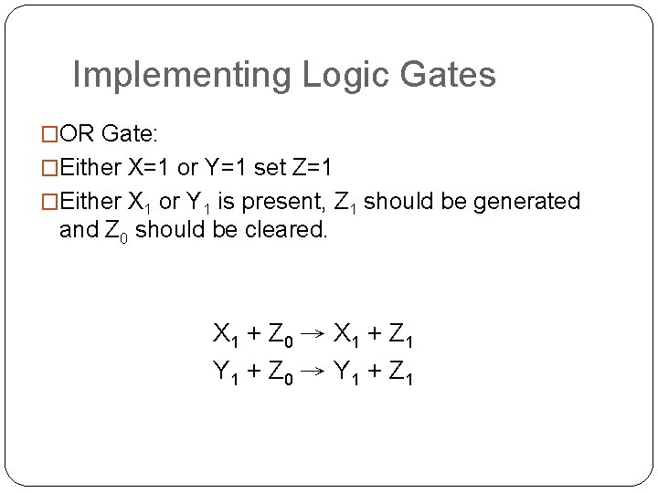
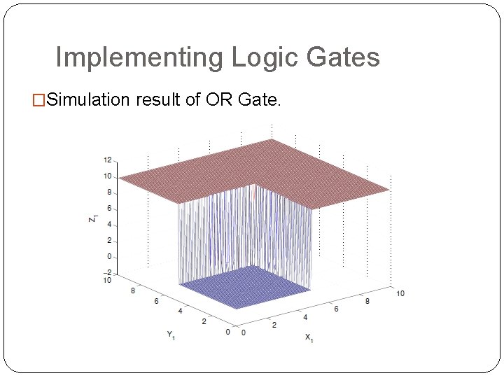
Implementing Logic Gates �OR Gate: �Either X=1 or Y=1 set Z=1 �Either X 1 or Y 1 is present, Z 1 should be generated and Z 0 should be cleared. X 1 + Z 0 → X 1 + Z 1 Y 1 + Z 0 → Y 1 + Z 1

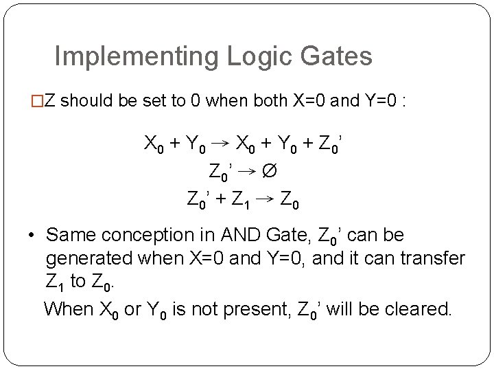
Implementing Logic Gates �Z should be set to 0 when both X=0 and Y=0 : X 0 + Y 0 → X 0 + Y 0 + Z 0’ → Ø Z 0’ + Z 1 → Z 0 • Same conception in AND Gate, Z 0’ can be generated when X=0 and Y=0, and it can transfer Z 1 to Z 0. When X 0 or Y 0 is not present, Z 0’ will be cleared.

Implementing Logic Gates �Simulation result of OR Gate.

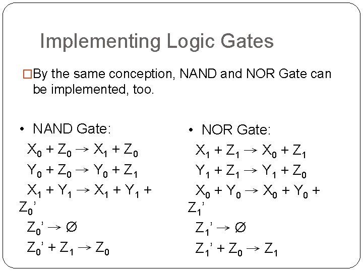
Implementing Logic Gates �By the same conception, NAND and NOR Gate can be implemented, too. • NAND Gate: X 0 + Z 0 → X 1 + Z 0 Y 0 + Z 0 → Y 0 + Z 1 X 1 + Y 1 → X 1 + Y 1 + Z 0’ → Ø Z 0’ + Z 1 → Z 0 • NOR Gate: X 1 + Z 1 → X 0 + Z 1 Y 1 + Z 1 → Y 1 + Z 0 X 0 + Y 0 → X 0 + Y 0 + Z 1’ → Ø Z 1’ + Z 0 → Z 1

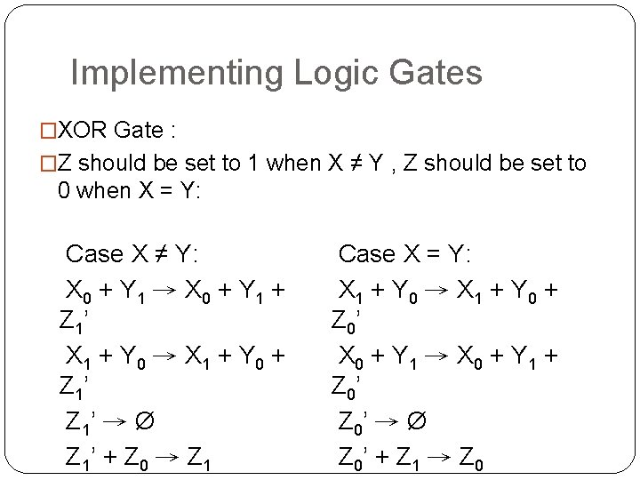
Implementing Logic Gates �XOR Gate : �Z should be set to 1 when X ≠ Y , Z should be set to 0 when X = Y: Case X ≠ Y: X 0 + Y 1 → X 0 + Y 1 + Z 1’ X 1 + Y 0 → X 1 + Y 0 + Z 1’ → Ø Z 1’ + Z 0 → Z 1 Case X = Y: X 1 + Y 0 → X 1 + Y 0 + Z 0’ X 0 + Y 1 → X 0 + Y 1 + Z 0’ → Ø Z 0’ + Z 1 → Z 0

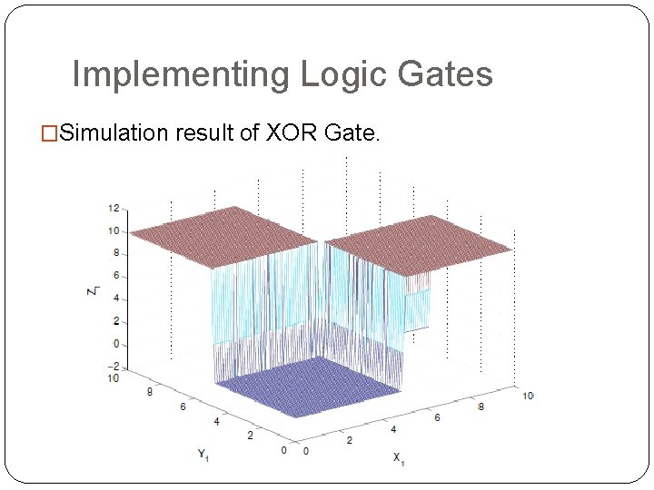
Implementing Logic Gates �Simulation result of XOR Gate.

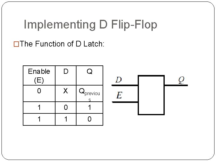
Implementing D Flip-Flop �The Function of D Latch: Enable (E) D Q 0 X Qpreviou s 1 0 1 1 1 0

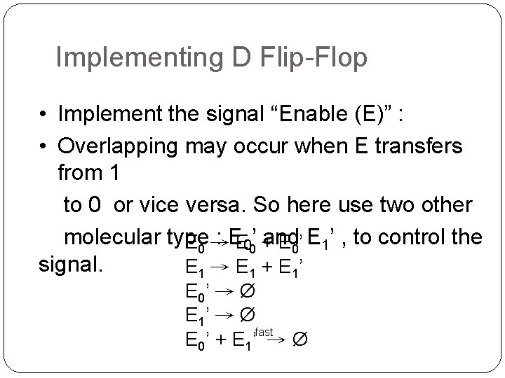
Implementing D Flip-Flop • Implement the signal “Enable (E)” : • Overlapping may occur when E transfers from 1 to 0 or vice versa. So here use two other molecular type : EE 00’ +and E 0 → E 0’ E 1’ , to control the signal. E 1 → E 1 + E 1’ E 0’ → Ø E 1’ → Ø fast E 0’ + E 1’ → Ø

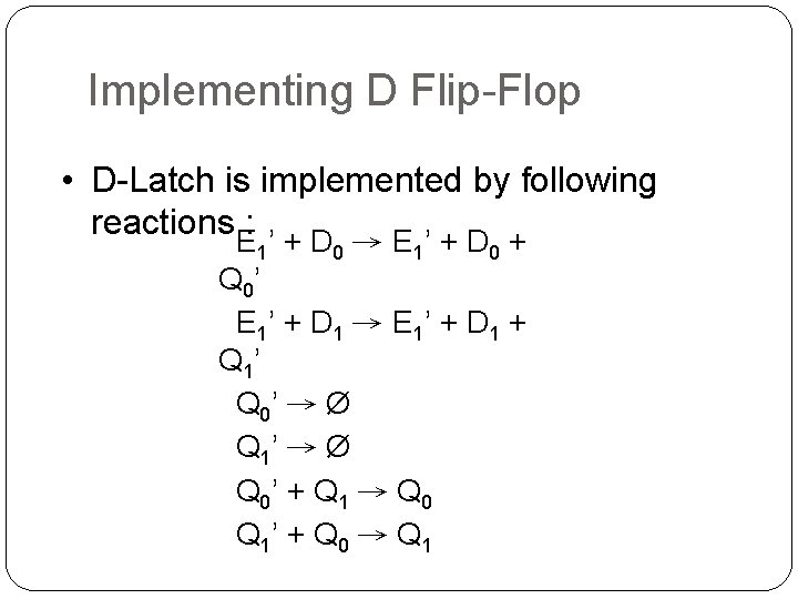
Implementing D Flip-Flop • D-Latch is implemented by following reactions. E: ’ + D → E ’ + D + 1 0 Q 0’ E 1’ + D 1 → E 1’ + D 1 + Q 1’ Q 0’ → Ø Q 1’ → Ø Q 0’ + Q 1 → Q 0 Q 1’ + Q 0 → Q 1

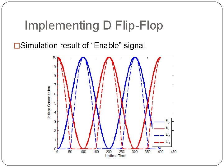
Implementing D Flip-Flop �Simulation result of “Enable” signal.

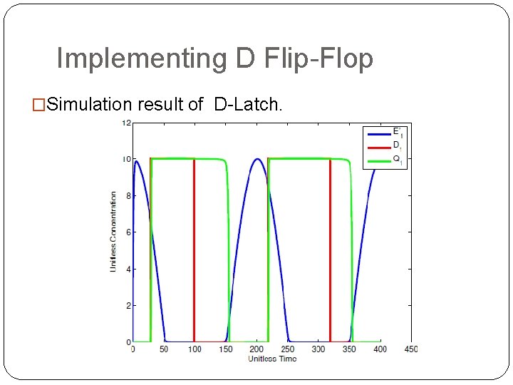
Implementing D Flip-Flop �Simulation result of D-Latch.

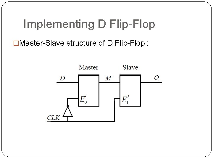
Implementing D Flip-Flop �Master-Slave structure of D Flip-Flop :

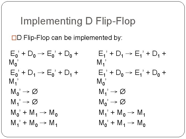
Implementing D Flip-Flop �D Flip-Flop can be implemented by: E 0’ + D 0 → E 0’ + D 0 + M 0 ’ E 0’ + D 1 → E 0’ + D 1 + M 1 ’ M 0 ’ → Ø M 1 ’ → Ø M 0 ’ + M 1 → M 0 M 1 ’ + M 0 → M 1 E 1’ + D 1 → E 1’ + D 1 + M 1 ’ E 1’ + D 0 → E 1’ + D 0 + M 0 ’ M 1 ’ → Ø M 0 ’ → Ø M 1 ’ + M 0 → M 1 M 0 ’ + M 1 → M 0

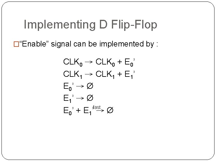
Implementing D Flip-Flop �“Enable” signal can be implemented by : CLK 0 → CLK 0 + E 0’ CLK 1 → CLK 1 + E 1’ E 0’ → Ø E 1’ → Ø fast E 0’ + E 1’ → Ø

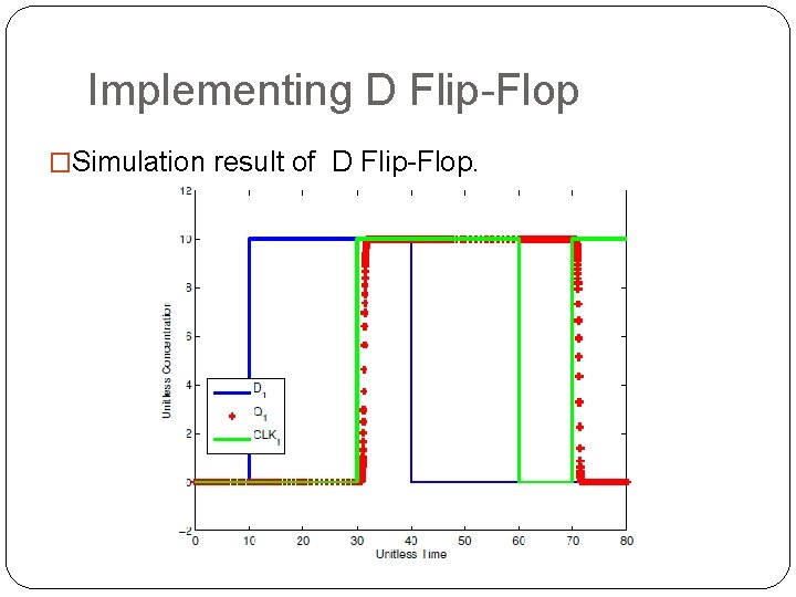
Implementing D Flip-Flop �Simulation result of D Flip-Flop.

Thank you