digital logic Operating Systems and Architecture UFCFCU30 1
- Slides: 27

<digital logic> Operating Systems and Architecture (UFCFCU-30 -1)

<outcomes> • After completing this section of the module you will be able to: • Describe and explain computer architecture, digital logic and machine level representation of data (number systems) • digital logic • static and dynamic digital systems

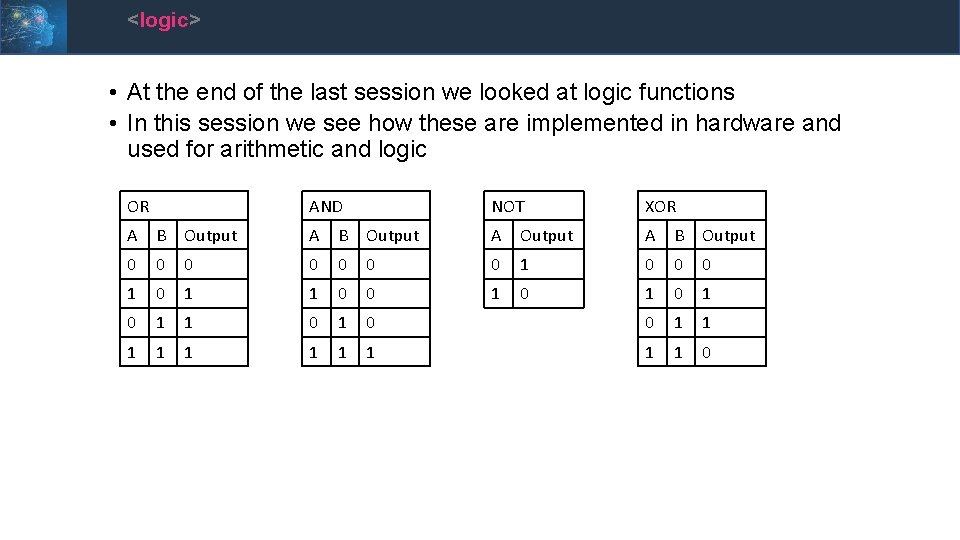
<logic> • At the end of the last session we looked at logic functions • In this session we see how these are implemented in hardware and used for arithmetic and logic OR AND NOT XOR A B Output A B Output 0 0 0 0 1 1 0 0 1 0 1 1 0 0 1 1 1 1 1 0

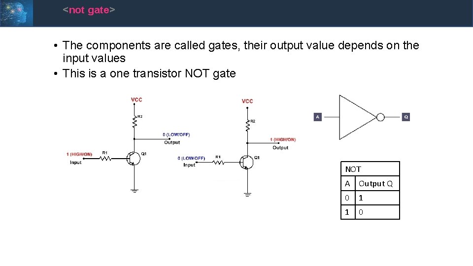
<not gate> • The components are called gates, their output value depends on the input values • This is a one transistor NOT gate NOT A Output Q 0 1 1 0

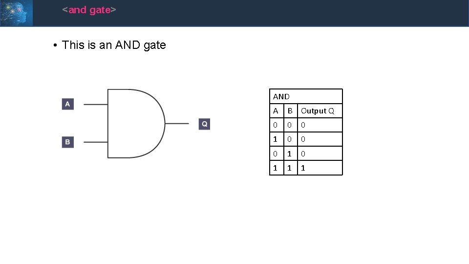
<and gate> • This is an AND gate AND A B Output Q 0 0 0 1 0 1 1 1

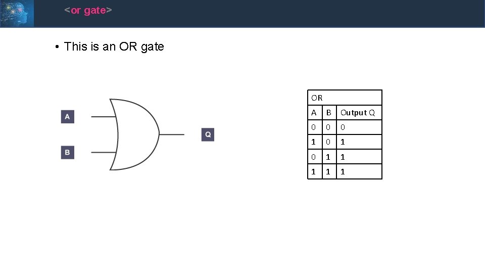
<or gate> • This is an OR gate OR A B Output Q 0 0 0 1 0 1 1 1

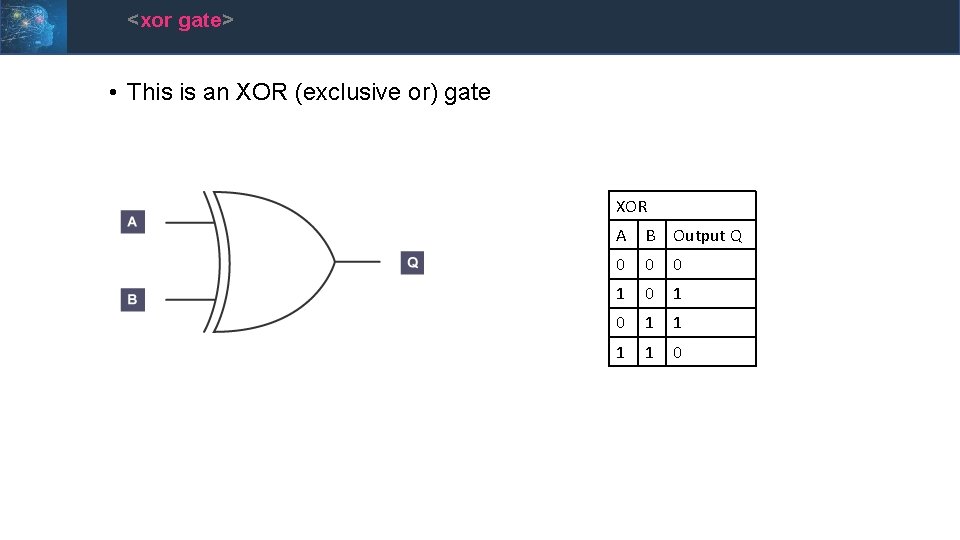
<xor gate> • This is an XOR (exclusive or) gate XOR A B Output Q 0 0 0 1 0 1 1 0

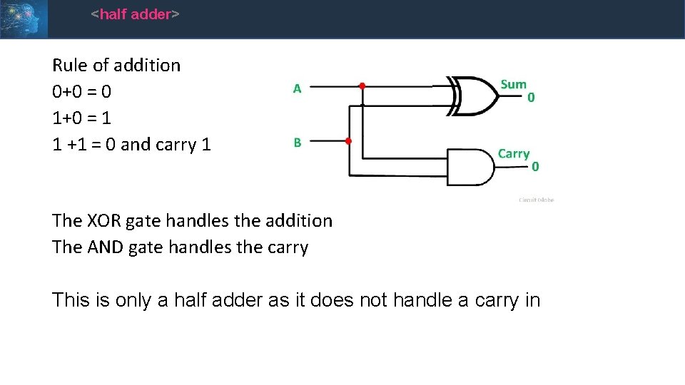
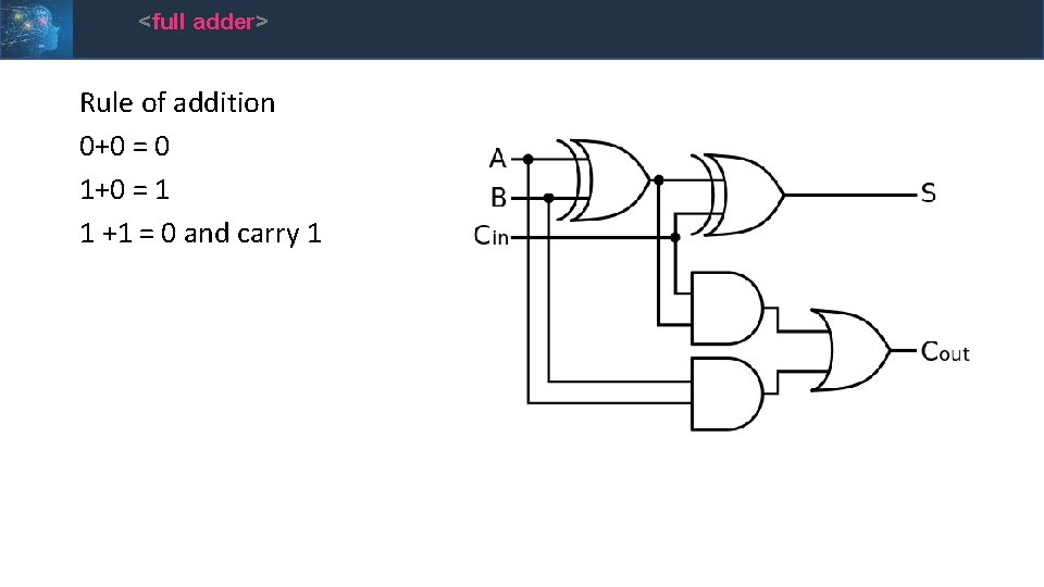
<half adder> Rule of addition 0+0 = 0 1+0 = 1 1 +1 = 0 and carry 1 The XOR gate handles the addition The AND gate handles the carry This is only a half adder as it does not handle a carry in

<full adder> Rule of addition 0+0 = 0 1+0 = 1 1 +1 = 0 and carry 1

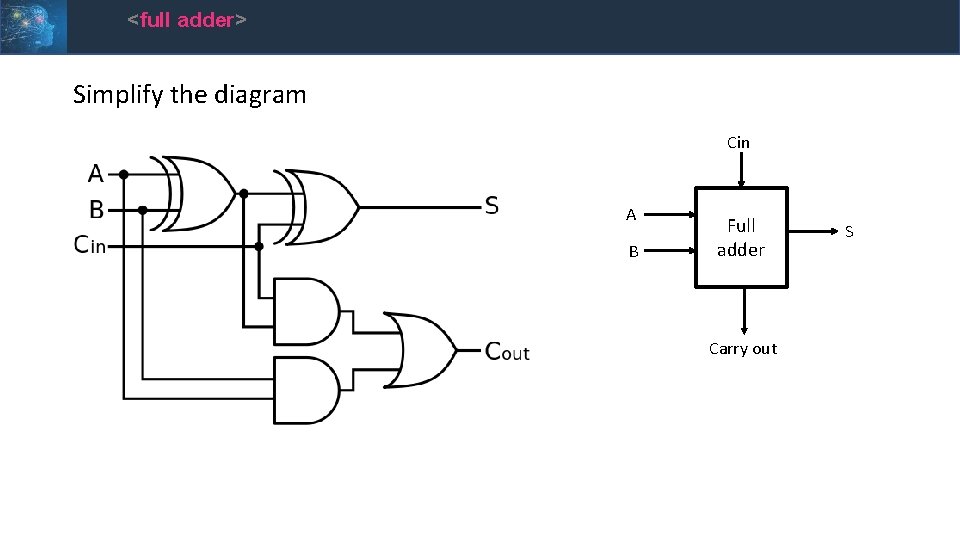
<full adder> Simplify the diagram Cin A B Full adder Carry out S

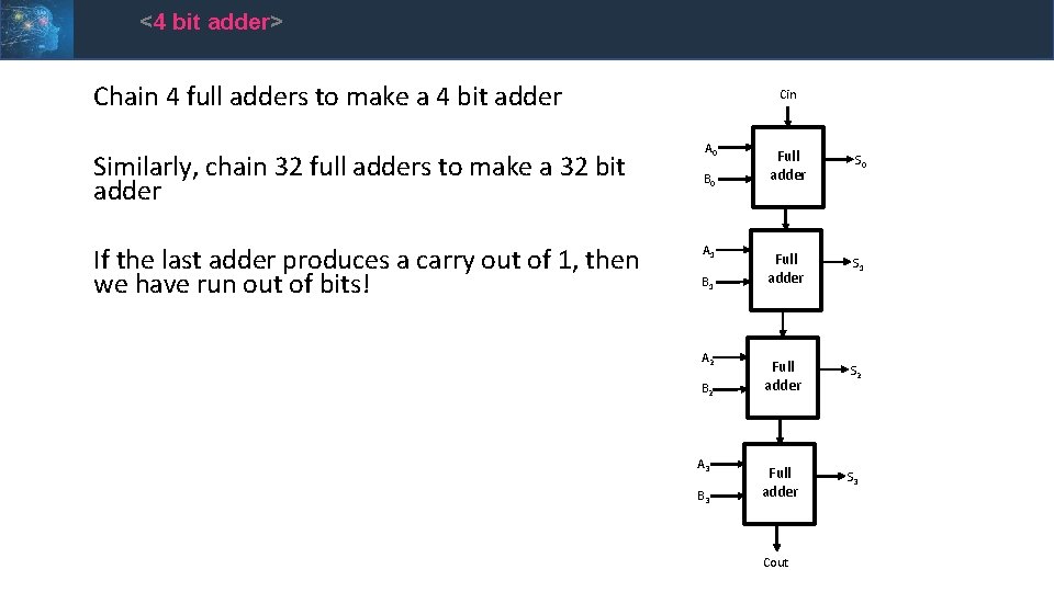
<4 bit adder> Chain 4 full adders to make a 4 bit adder Similarly, chain 32 full adders to make a 32 bit adder If the last adder produces a carry out of 1, then we have run out of bits! Cin A 0 B 0 A 1 B 1 A 2 B 2 A 3 B 3 Full adder S 0 Full adder S 1 Full adder S 2 Full adder S 3 Cout

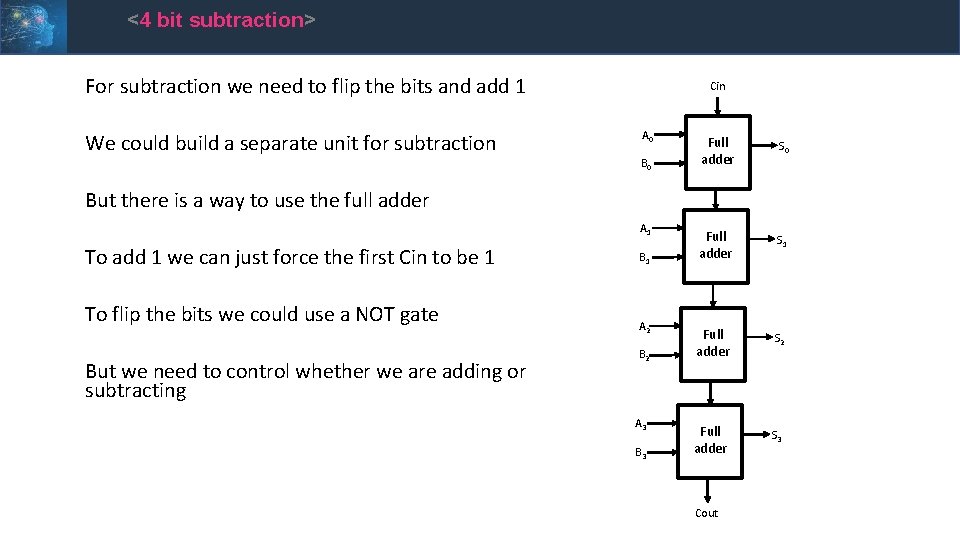
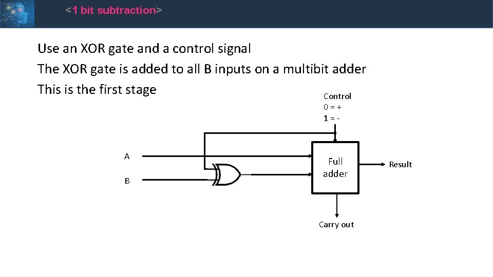
<4 bit subtraction> For subtraction we need to flip the bits and add 1 We could build a separate unit for subtraction Cin A 0 B 0 Full adder S 1 Full adder S 2 Full adder S 3 But there is a way to use the full adder A 1 To add 1 we can just force the first Cin to be 1 To flip the bits we could use a NOT gate But we need to control whether we are adding or subtracting B 1 A 2 B 2 A 3 B 3 Cout

<1 bit subtraction> Use an XOR gate and a control signal The XOR gate is added to all B inputs on a multibit adder This is the first stage Control 0=+ 1=- A B Full adder Carry out Result

<progress> • So far: • We have a unit that can add and subtract • We have introduced the concept of control • Where do the inputs come from and where does the output go? • We need to store data

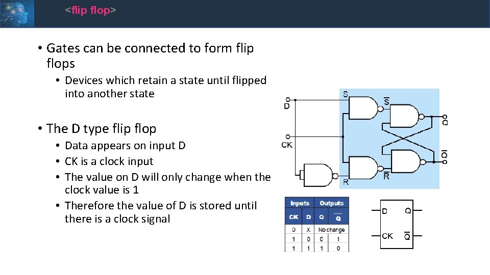
<flip flop> • Gates can be connected to form flip flops • Devices which retain a state until flipped into another state • The D type flip flop • Data appears on input D • CK is a clock input • The value on D will only change when the clock value is 1 • Therefore the value of D is stored until there is a clock signal

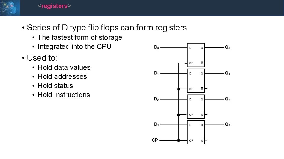
<registers> • Series of D type flip flops can form registers • The fastest form of storage • Integrated into the CPU • Used to: • • Hold data values Hold addresses Hold status Hold instructions

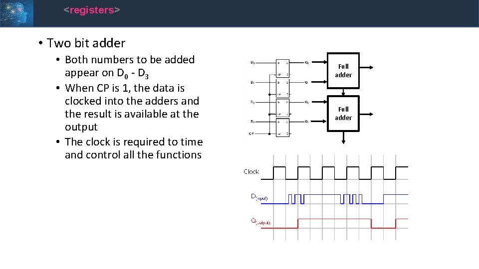
<registers> • Two bit adder • Both numbers to be added appear on D 0 - D 3 • When CP is 1, the data is clocked into the adders and the result is available at the output • The clock is required to time and control all the functions Full adder

<s. RAM> • Arrays of D type flip flops are called SRAM • RAM for Random Access Memory • S for static • So long as power is applied, SRAM will retain its value, it does not need to be refreshed • This means all accesses are for required functions, and are not overhead

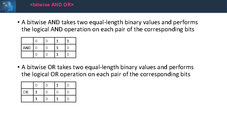
<bitwise AND OR> • A bitwise AND takes two equal-length binary values and performs the logical AND operation on each pair of the corresponding bits AND 0 0 1 1 0 0 0 1 0 • A bitwise OR takes two equal-length binary values and performs the logical OR operation on each pair of the corresponding bits OR 0 0 1 0 1 0

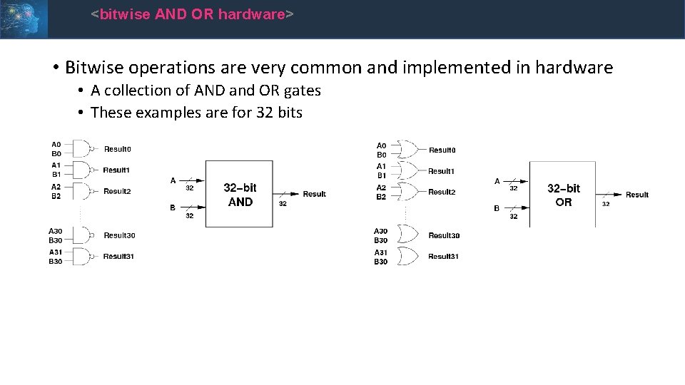
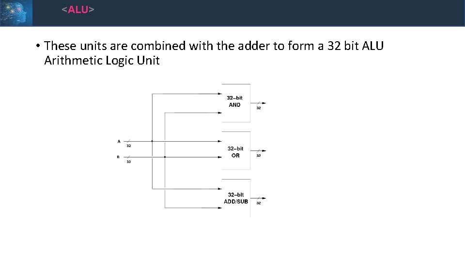
<bitwise AND OR hardware> • Bitwise operations are very common and implemented in hardware • A collection of AND and OR gates • These examples are for 32 bits

<ALU> • These units are combined with the adder to form a 32 bit ALU Arithmetic Logic Unit

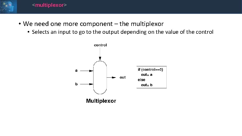
<multiplexor> • We need one more component – the multiplexor • Selects an input to go to the output depending on the value of the control

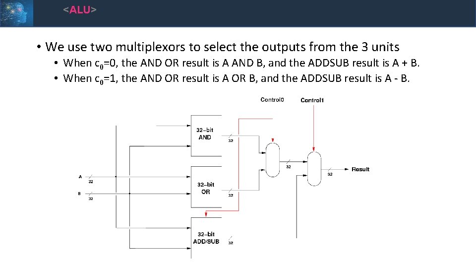
<ALU> • We use two multiplexors to select the outputs from the 3 units • When c 0=0, the AND OR result is A AND B, and the ADDSUB result is A + B. • When c 0=1, the AND OR result is A OR B, and the ADDSUB result is A - B.

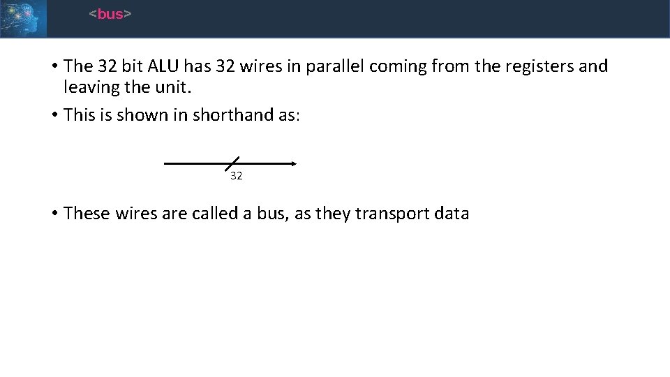
<bus> • The 32 bit ALU has 32 wires in parallel coming from the registers and leaving the unit. • This is shown in shorthand as: 32 • These wires are called a bus, as they transport data

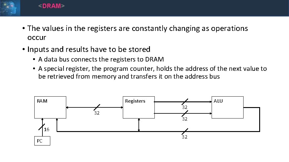
<DRAM> • The values in the registers are constantly changing as operations occur • Inputs and results have to be stored • A data bus connects the registers to DRAM • A special register, the program counter, holds the address of the next value to be retrieved from memory and transfers it on the address bus Registers RAM 32 32 32 16 PC 32 ALU

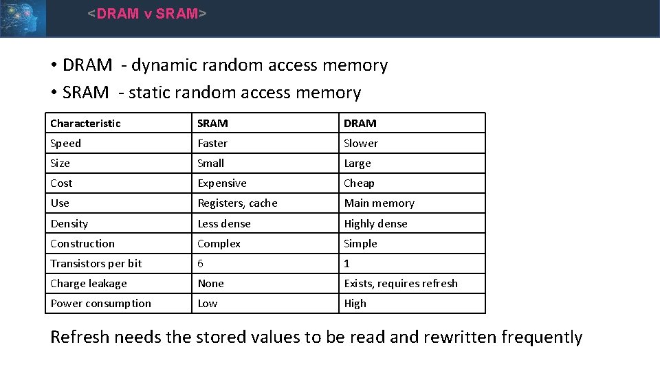
<DRAM v SRAM> • DRAM - dynamic random access memory • SRAM - static random access memory Characteristic SRAM DRAM Speed Faster Slower Size Small Large Cost Expensive Cheap Use Registers, cache Main memory Density Less dense Highly dense Construction Complex Simple Transistors per bit 6 1 Charge leakage None Exists, requires refresh Power consumption Low High Refresh needs the stored values to be read and rewritten frequently

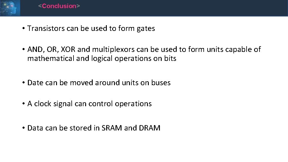
<Conclusion> • Transistors can be used to form gates • AND, OR, XOR and multiplexors can be used to form units capable of mathematical and logical operations on bits • Date can be moved around units on buses • A clock signal can control operations • Data can be stored in SRAM and DRAM