Digital Logic Design Lecture 21 Announcements Homework 7


- Slides: 30

Digital Logic Design Lecture 21

Announcements • Homework 7 due on Thursday, 11/13 • Recitation quiz on Monday on material from Lectures 21, 22

Agenda • Last time: – Multiplexers (5. 6) • This time: – Programmable Logic Devices (5. 7) – Programmable Read-Only Memories (PROM) (5. 8) – Programmable Logic Arrays (PLAs) (5. 9) – Programmable Array Logic (PAL) (5. 10)

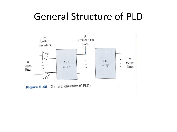
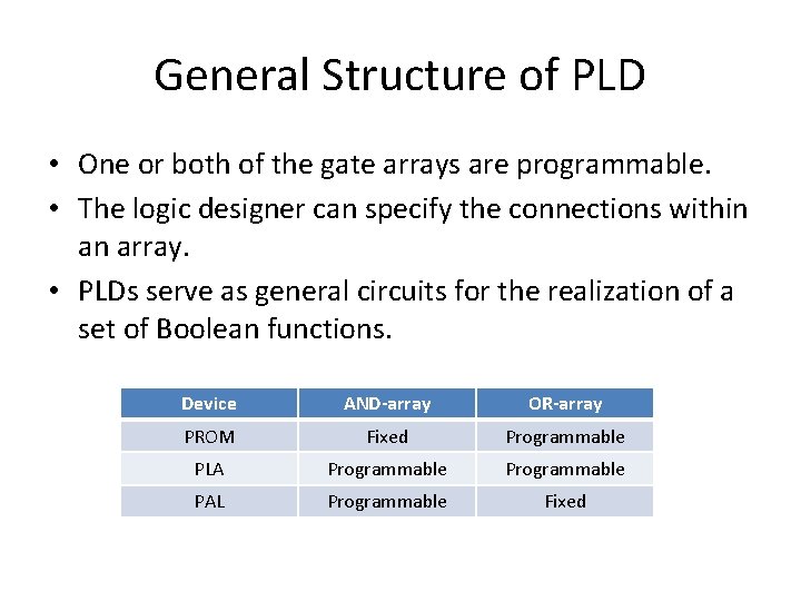
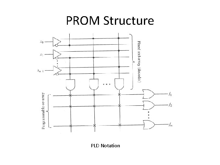
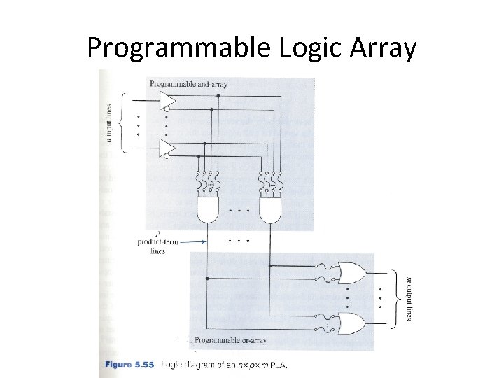
General Structure of PLD • Inputs to the PLD are applied to a set of buffer/inverters. These devices have both the true value of the input as well as the complemented value of the input as its outputs. • Outputs from these devices are the inputs to an array of and-gates. The AND array generates a set of p product terms. • The product terms are inputs to an array of orgates to realize a set of m sum-of-product expressions.

General Structure of PLD

General Structure of PLD • One or both of the gate arrays are programmable. • The logic designer can specify the connections within an array. • PLDs serve as general circuits for the realization of a set of Boolean functions. Device AND-array OR-array PROM Fixed Programmable PLA Programmable PAL Programmable Fixed

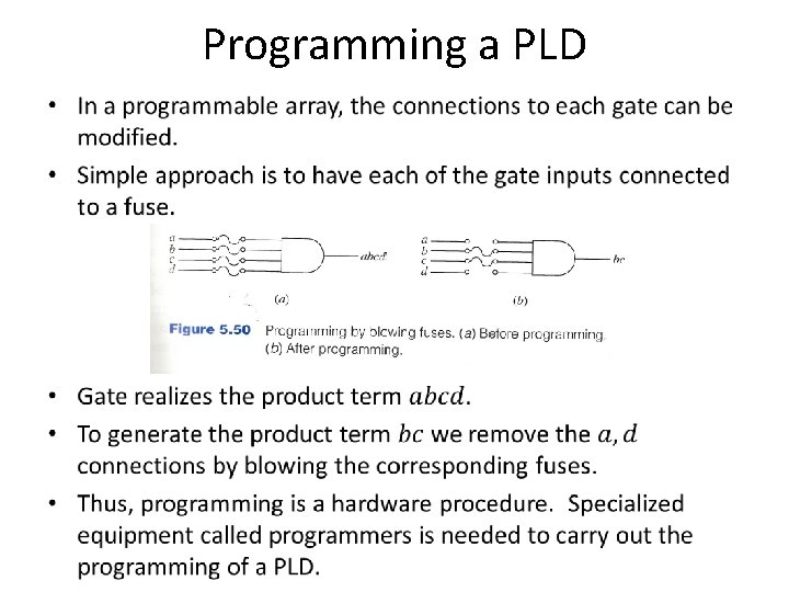
Programming a PLD •

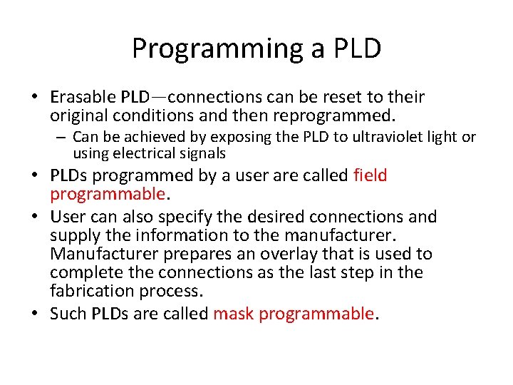
Programming a PLD • Erasable PLD—connections can be reset to their original conditions and then reprogrammed. – Can be achieved by exposing the PLD to ultraviolet light or using electrical signals • PLDs programmed by a user are called field programmable. • User can also specify the desired connections and supply the information to the manufacturer. Manufacturer prepares an overlay that is used to complete the connections as the last step in the fabrication process. • Such PLDs are called mask programmable.

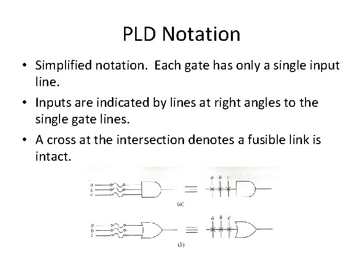
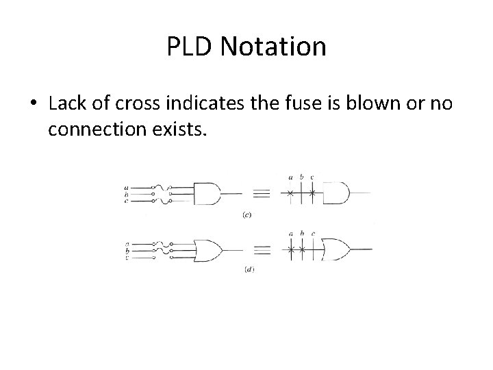
PLD Notation • Simplified notation. Each gate has only a single input line. • Inputs are indicated by lines at right angles to the single gate lines. • A cross at the intersection denotes a fusible link is intact.

PLD Notation • Lack of cross indicates the fuse is blown or no connection exists.

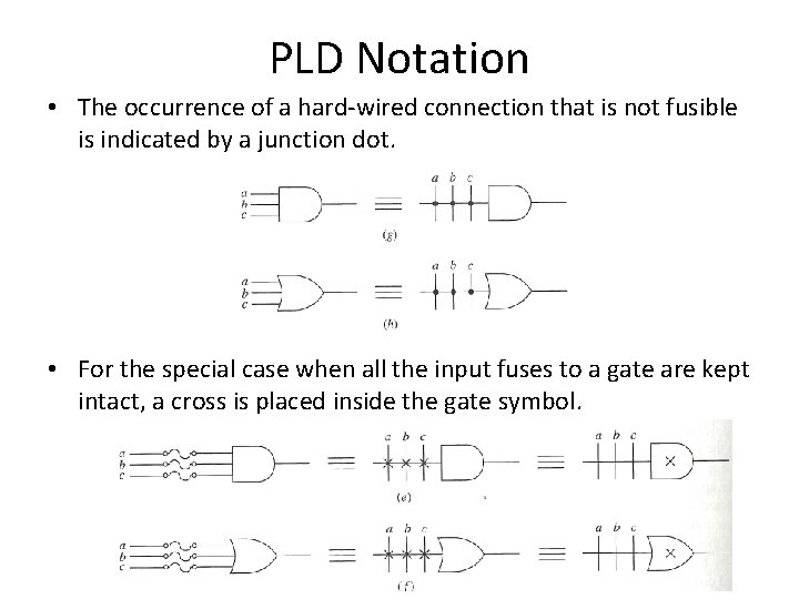
PLD Notation • The occurrence of a hard-wired connection that is not fusible is indicated by a junction dot. • For the special case when all the input fuses to a gate are kept intact, a cross is placed inside the gate symbol.

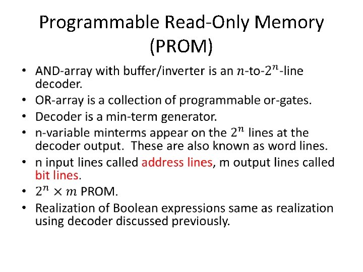
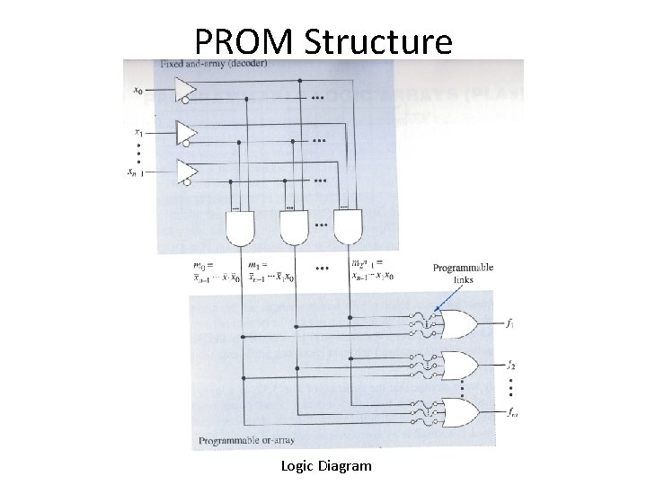
Programmable Read-Only Memory (PROM) •

PROM Structure Logic Diagram

PROM Structure PLD Notation

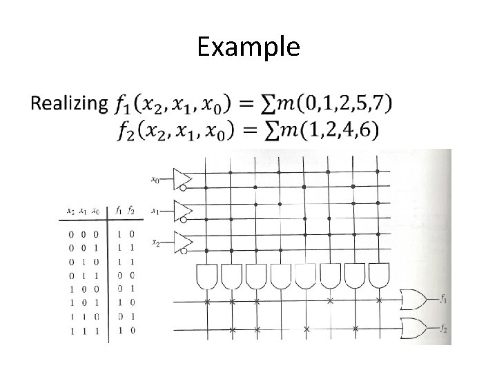
Example •

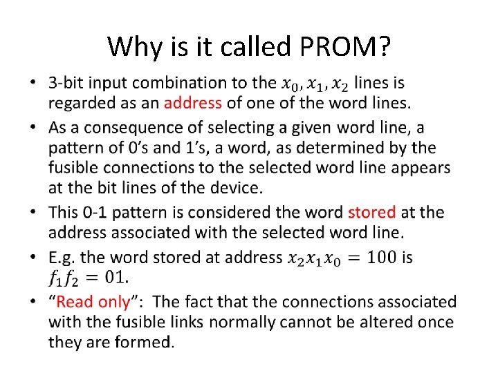
Why is it called PROM? •

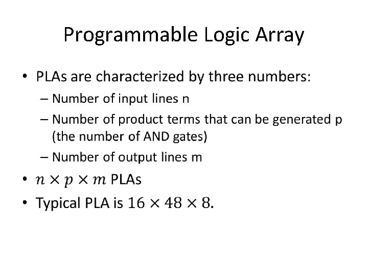
Programmable Logic Array •

Programmable Logic Array

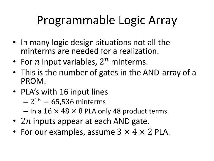
Programmable Logic Array •

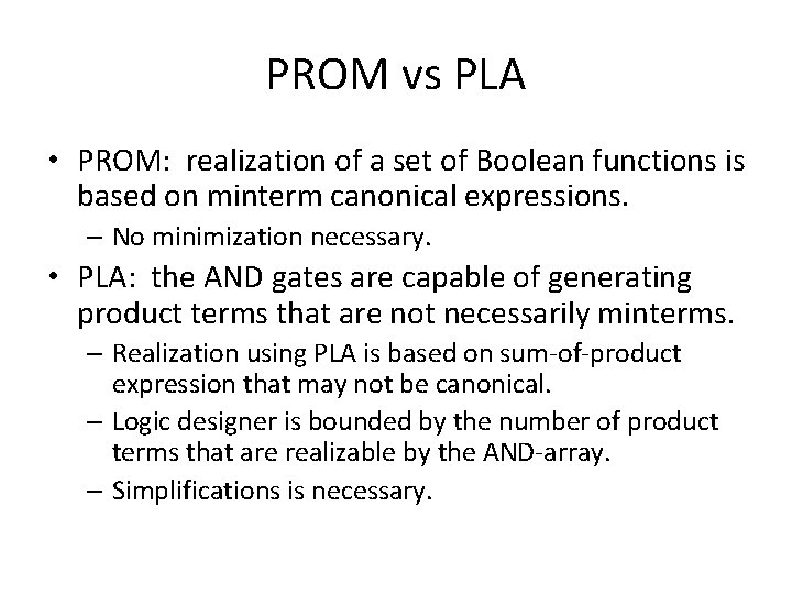
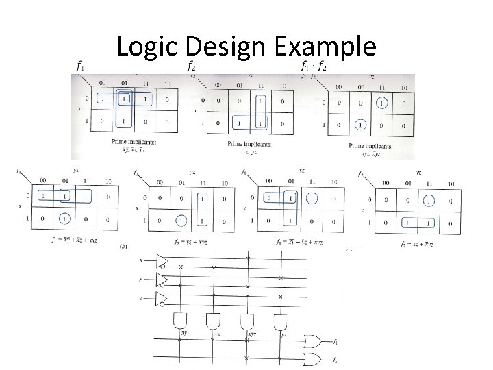
PROM vs PLA • PROM: realization of a set of Boolean functions is based on minterm canonical expressions. – No minimization necessary. • PLA: the AND gates are capable of generating product terms that are not necessarily minterms. – Realization using PLA is based on sum-of-product expression that may not be canonical. – Logic designer is bounded by the number of product terms that are realizable by the AND-array. – Simplifications is necessary.

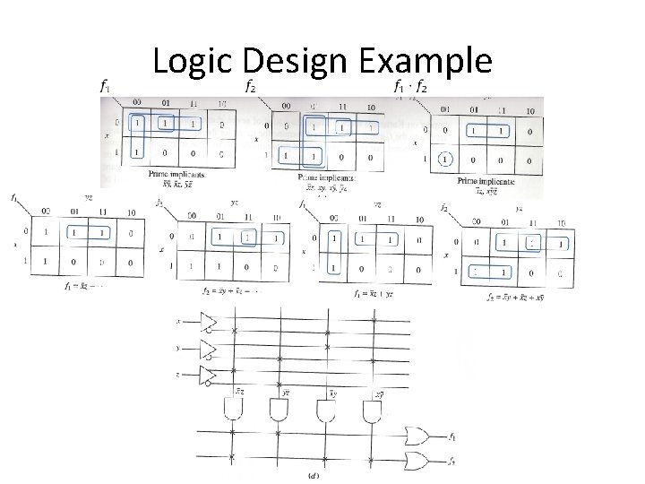
Logic Design Example

Logic Design Example

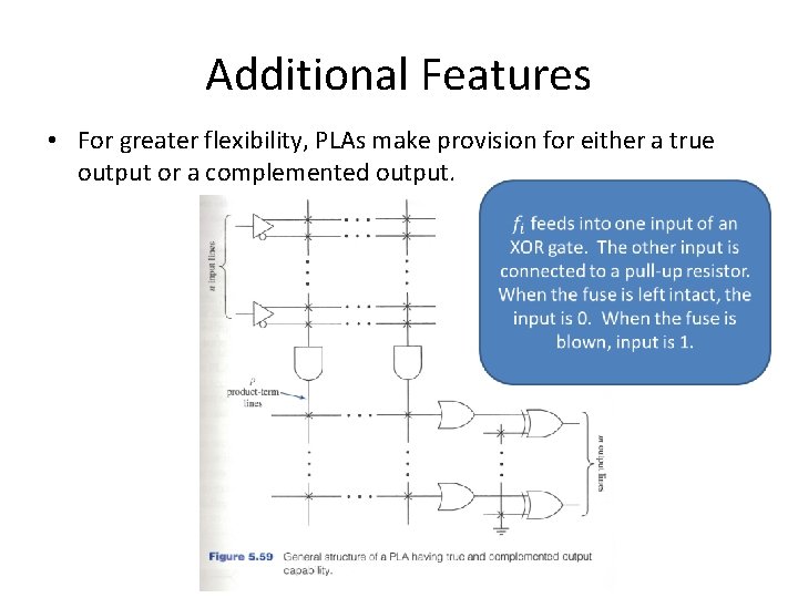
Additional Features • For greater flexibility, PLAs make provision for either a true output or a complemented output.

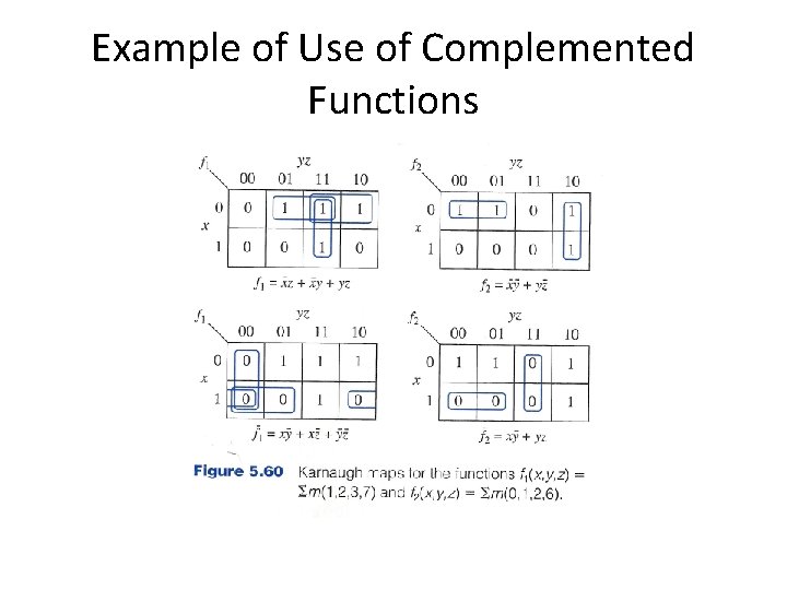
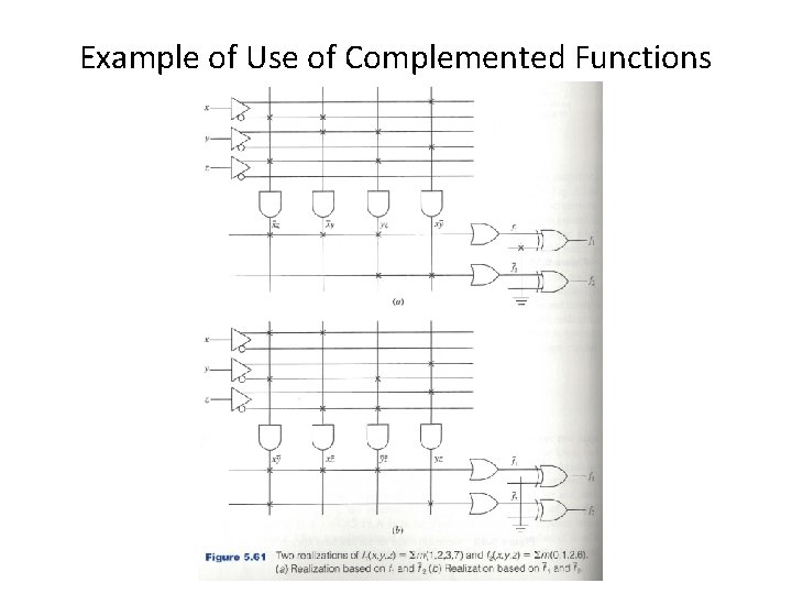
Example of Use of Complemented Functions

Example of Use of Complemented Functions

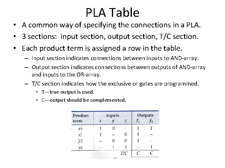
PLA Table • A common way of specifying the connections in a PLA. • 3 sections: input section, output section, T/C section. • Each product term is assigned a row in the table. – Input section indicates connections between inputs to AND-array. – Output section indicates connections between outputs of AND-array and inputs to the OR-array. – T/C section indicates how the exclusive or gates are programmed. • T—true output is used. • C—output should be complemented.

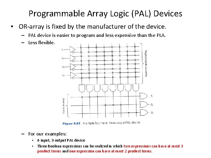
Programmable Array Logic (PAL) Devices • OR-array is fixed by the manufacturer of the device. – PAL device is easier to program and less expensive than the PLA. – Less flexible. – For our examples: • 4 -input, 3 -output PAL device • Three Boolean expressions can be realized in which two expressions can have at most 3 product terms and one expression can have at most 2 product terms.

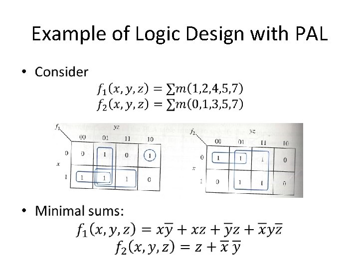
Example of Logic Design with PAL •

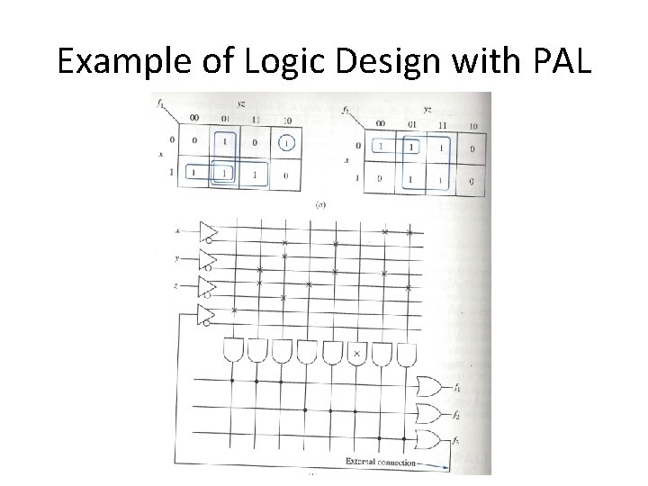
Example of Logic Design with PAL
