Digital Logic Design I Synchronous Sequential Logic Mustafa




- Slides: 71

Digital Logic Design I Synchronous Sequential Logic Mustafa Kemal Uyguroğlu

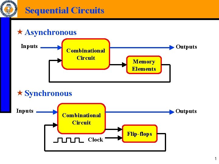
Sequential Circuits « Asynchronous Inputs Combinational Circuit Outputs Memory Elements « Synchronous Inputs Outputs Combinational Circuit Clock Flip-flops 1

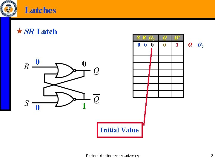
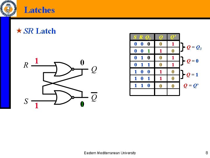
Latches « SR Latch S R Q 0 0 0 0 1 Q 0 Q’ 1 Q = Q 0 Initial Value Eastern Mediterranean University 2

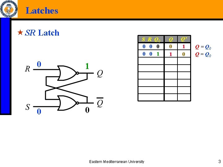
Latches « SR Latch S R Q 0 0 0 1 0 0 Eastern Mediterranean University Q 0 1 Q’ 1 0 Q = Q 0 3

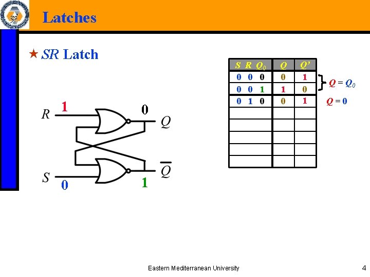
Latches « SR Latch 1 0 0 1 S 0 0 0 Eastern Mediterranean University R 0 0 1 Q 0 0 1 0 Q’ 1 0 1 Q = Q 0 Q=0 4

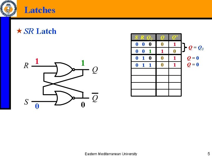
Latches « SR Latch 1 1 0 0 S 0 0 Eastern Mediterranean University R 0 0 1 1 Q 0 0 1 Q 0 1 0 0 Q’ 1 0 1 1 Q = Q 0 Q=0 5

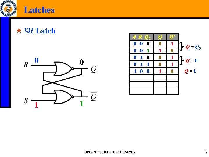
Latches « SR Latch 0 1 0 S 0 0 1 R 0 0 1 1 0 Q 0 0 1 0 Q 0 1 0 0 1 Q’ 1 0 1 1 0 Q = Q 0 Q=1 1 Eastern Mediterranean University 6

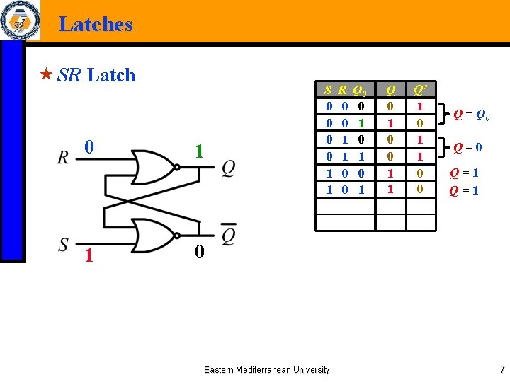
Latches « SR Latch 0 1 1 S 0 0 1 1 R 0 0 1 1 0 0 Q 0 0 1 0 1 Q 0 1 0 0 1 1 Q’ 1 0 1 1 0 0 Q = Q 0 Q=1 Q=1 0 Eastern Mediterranean University 7

Latches « SR Latch 1 1 0 S 0 0 1 1 1 R 0 0 1 1 0 0 1 Q 0 0 1 0 1 0 Q 0 1 0 0 1 1 0 Q’ 1 0 1 1 0 0 0 Q = Q 0 Q=1 Q = Q’ 10 Eastern Mediterranean University 8

Latches « SR Latch 1 1 10 S 0 0 1 1 R 0 0 1 1 Q 0 0 1 0 1 Q 0 1 0 0 1 1 0 0 Q’ 1 0 1 1 0 0 Q = Q 0 Q=1 Q = Q’ 0 Eastern Mediterranean University 9

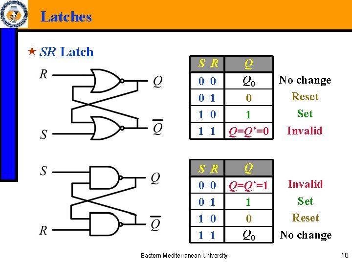
Latches « SR Latch S R Q Q 0 No change Reset 0 Set 1 Invalid Q=Q’=0 0 0 1 1 0 1 S 0 0 1 1 Q R Invalid 0 Q=Q’=1 Set 1 1 Reset 0 0 Q 0 No change 1 Eastern Mediterranean University 10

Latches « SR Latch S R 0 0 1 1 0 1 S’ R’ 0 0 1 1 0 1 Eastern Mediterranean University Q Q 0 No change Reset 0 Set 1 Invalid Q=Q’=0 Q Invalid Q=Q’=1 Set 1 Reset 0 Q 0 No change 11

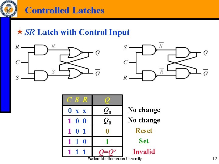
Controlled Latches « SR Latch with Control Input C S R 0 1 1 x 0 1 Q Q 0 0 1 Q=Q’ No change Reset Set Invalid Eastern Mediterranean University 12

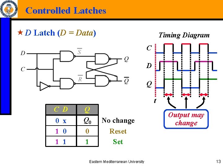
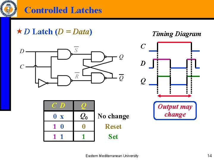
Controlled Latches « D Latch (D = Data) Timing Diagram C D Q t C D 0 x 1 0 1 1 Q Q 0 0 1 No change Reset Set Eastern Mediterranean University Output may change 13

Controlled Latches « D Latch (D = Data) Timing Diagram C D Q C D 0 x 1 0 1 1 Q Q 0 0 1 No change Reset Set Eastern Mediterranean University Output may change 14

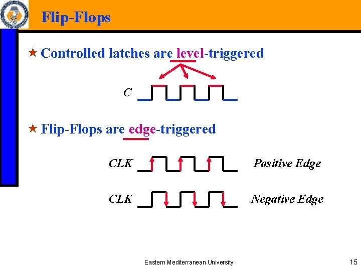
Flip-Flops « Controlled latches are level-triggered C « Flip-Flops are edge-triggered CLK Positive Edge CLK Negative Edge Eastern Mediterranean University 15

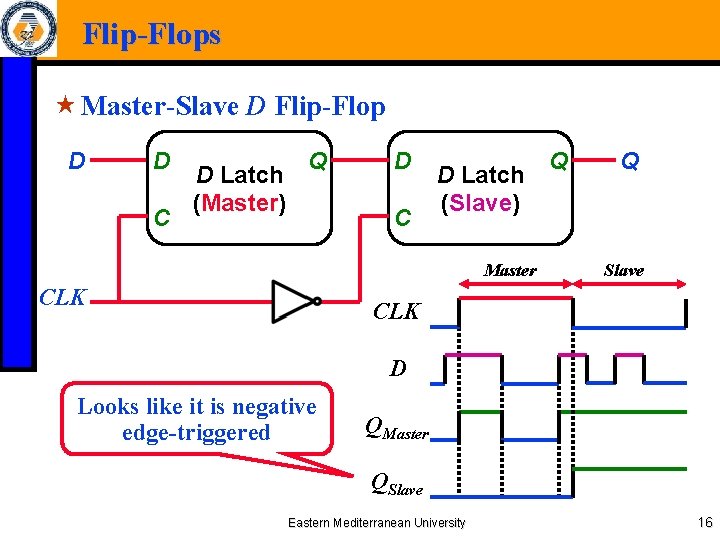
Flip-Flops « Master-Slave D Flip-Flop D D C D Latch (Master) Q D C D Latch (Slave) Master CLK Q Q Slave CLK D Looks like it is negative edge-triggered QMaster QSlave Eastern Mediterranean University 16

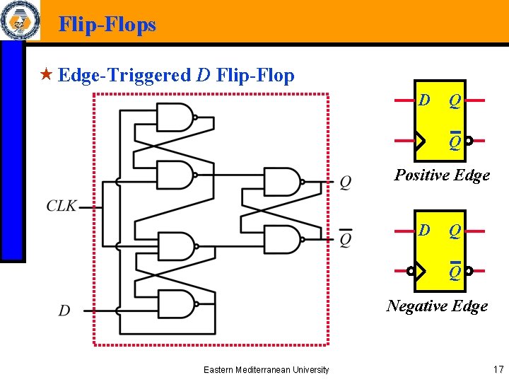
Flip-Flops « Edge-Triggered D Flip-Flop D Q Q Positive Edge D Q Q Negative Edge Eastern Mediterranean University 17

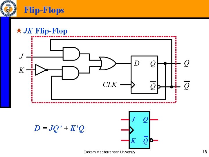
Flip-Flops « JK Flip-Flop J Q K Q D = JQ’ + K’Q Eastern Mediterranean University 18

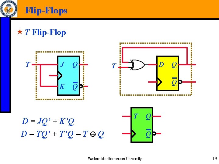
Flip-Flops « T Flip-Flop T J K Q D T Q Q Q T D = JQ’ + K’Q D = TQ’ + T’Q = T Q Eastern Mediterranean University Q Q 19

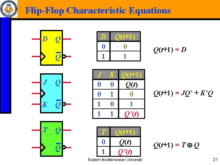
Flip-Flop Characteristic Tables D Q Q J Q K Q T Q Q D 0 1 J 0 0 1 1 T 0 1 Q(t+1) 0 1 Reset Set K Q(t+1) 0 Q(t) 1 0 0 1 1 Q’(t) No change Reset Set Toggle Q(t+1) Q(t) Q’(t) No change Toggle Eastern Mediterranean University 20

Flip-Flop Characteristic Equations D Q Q J Q K Q T Q Q D 0 1 J 0 0 1 1 Q(t+1) 0 1 K Q(t+1) 0 Q(t) 1 0 0 1 1 Q’(t) T 0 1 Q(t+1) Q(t) Q’(t) Eastern Mediterranean University Q(t+1) = D Q(t+1) = JQ’ + K’Q Q(t+1) = T Q 21

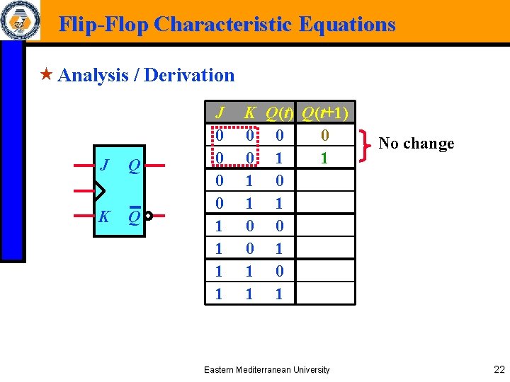
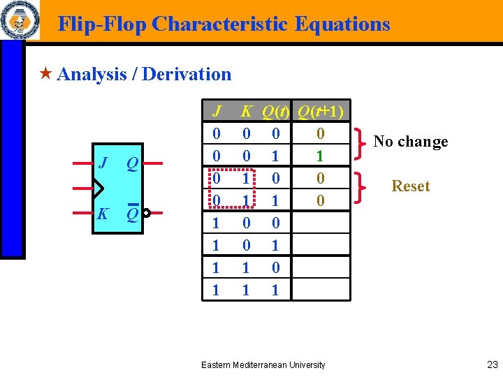
Flip-Flop Characteristic Equations « Analysis / Derivation J K Q Q J 0 0 1 1 K Q(t) Q(t+1) 0 0 1 1 1 0 0 0 1 1 Eastern Mediterranean University No change Reset Set Toggle 22

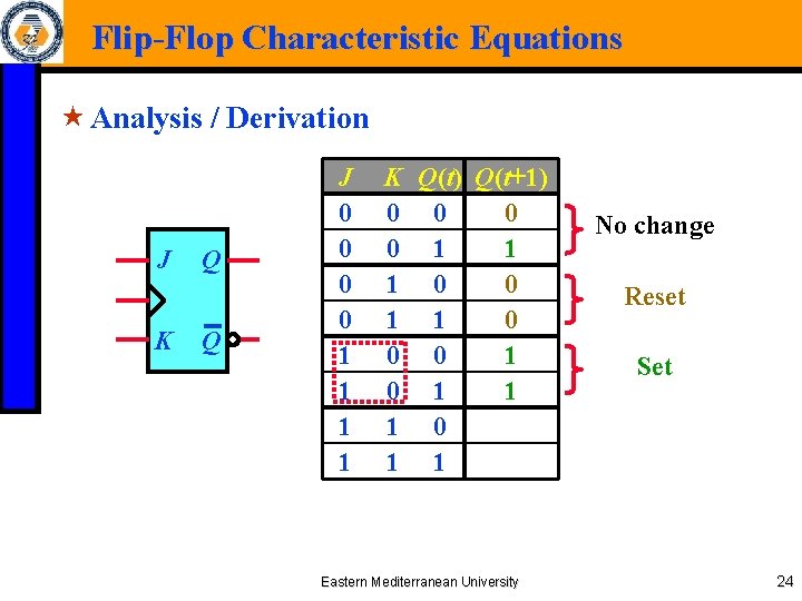
Flip-Flop Characteristic Equations « Analysis / Derivation J K Q Q J 0 0 1 1 K Q(t) Q(t+1) 0 0 1 1 1 0 0 0 0 1 1 Eastern Mediterranean University No change Reset Set Toggle 23

Flip-Flop Characteristic Equations « Analysis / Derivation J K Q Q J 0 0 1 1 K Q(t) Q(t+1) 0 0 1 1 1 0 1 1 Eastern Mediterranean University No change Reset Set Toggle 24

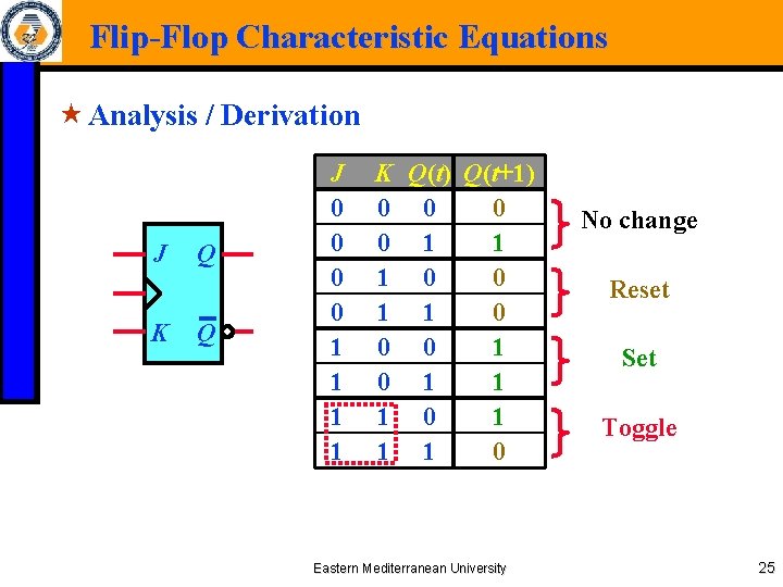
Flip-Flop Characteristic Equations « Analysis / Derivation J K Q Q J 0 0 1 1 K Q(t) Q(t+1) 0 0 1 1 1 0 1 1 1 0 Eastern Mediterranean University No change Reset Set Toggle 25

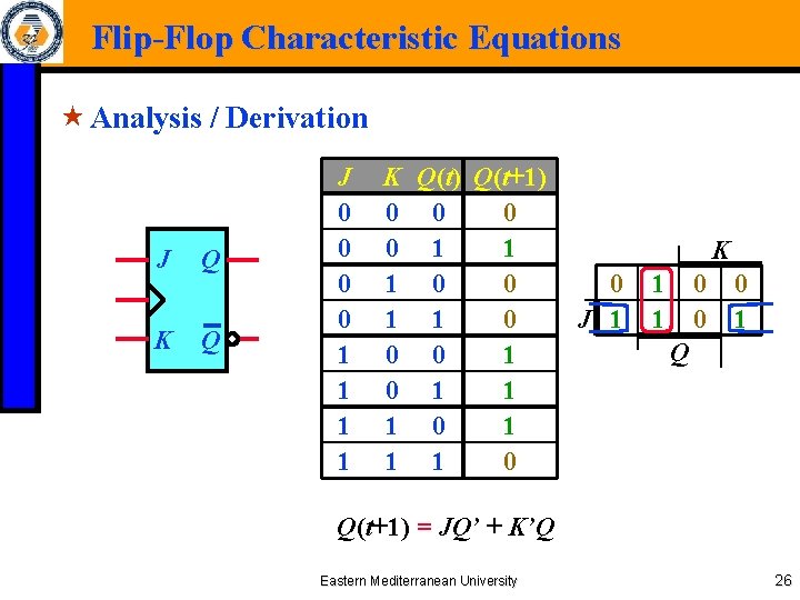
Flip-Flop Characteristic Equations « Analysis / Derivation J Q K Q J 0 0 1 1 K Q(t) Q(t+1) 0 0 1 1 1 0 1 1 1 0 K 0 J 1 1 1 0 0 0 1 Q Q(t+1) = JQ’ + K’Q Eastern Mediterranean University 26

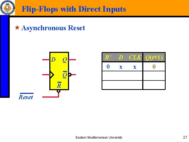
Flip-Flops with Direct Inputs « Asynchronous Reset D Q R’ 0 D CLK Q(t+1) x x 0 Q R Reset Eastern Mediterranean University 27

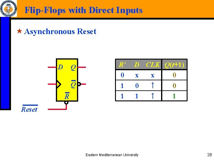
Flip-Flops with Direct Inputs « Asynchronous Reset D Q Q R R’ 0 1 1 D CLK Q(t+1) x x 0 ↑ 0 0 ↑ 1 1 Reset Eastern Mediterranean University 28

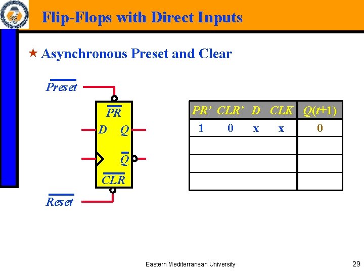
Flip-Flops with Direct Inputs « Asynchronous Preset and Clear Preset PR D Q PR’ CLR’ D CLK Q(t+1) 1 0 x x 0 Q CLR Reset Eastern Mediterranean University 29

Flip-Flops with Direct Inputs « Asynchronous Preset and Clear Preset PR D Q PR’ CLR’ D CLK Q(t+1) 1 0 x x 0 1 x 1 Q CLR Reset Eastern Mediterranean University 30

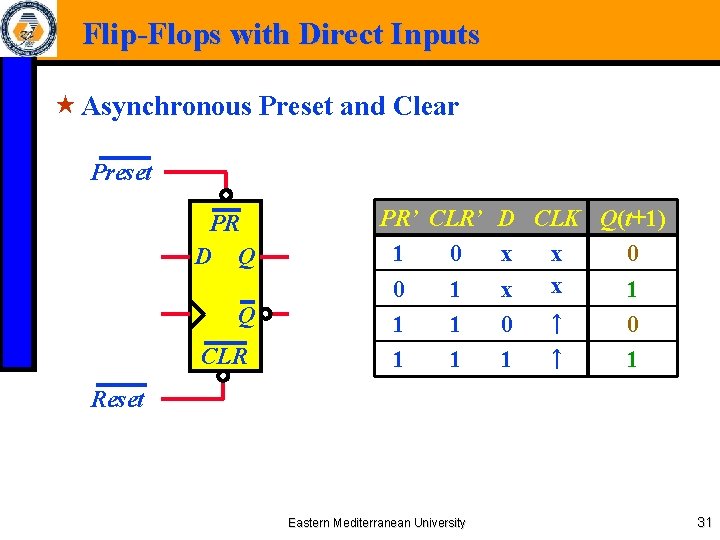
Flip-Flops with Direct Inputs « Asynchronous Preset and Clear Preset PR D Q Q CLR PR’ CLR’ D CLK Q(t+1) 1 0 x x 0 1 x 1 ↑ 1 1 0 0 ↑ 1 1 Reset Eastern Mediterranean University 31

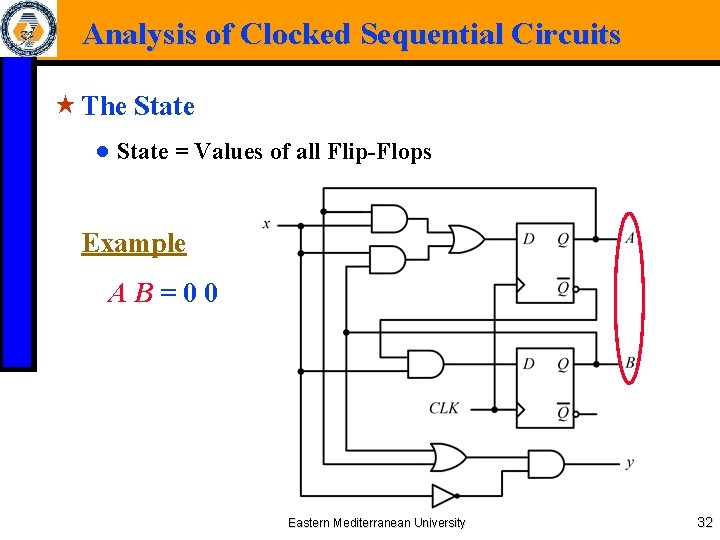
Analysis of Clocked Sequential Circuits « The State ● State = Values of all Flip-Flops Example AB=00 Eastern Mediterranean University 32

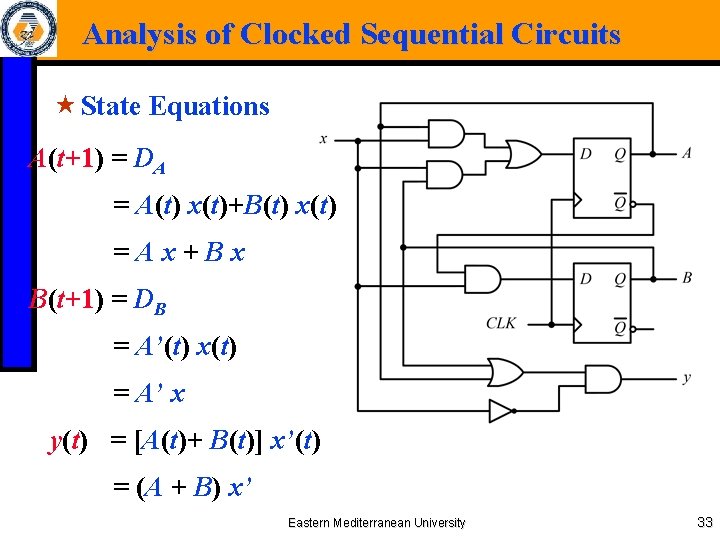
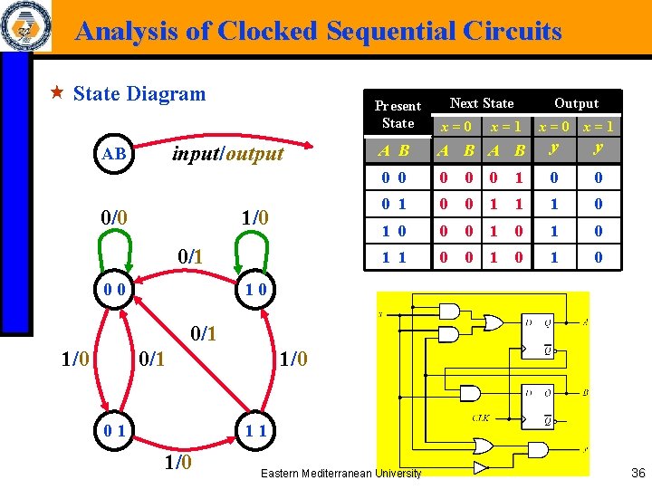
Analysis of Clocked Sequential Circuits « State Equations A(t+1) = DA = A(t) x(t)+B(t) x(t) =Ax+Bx B(t+1) = DB = A’(t) x(t) = A’ x y(t) = [A(t)+ B(t)] x’(t) = (A + B) x’ Eastern Mediterranean University 33

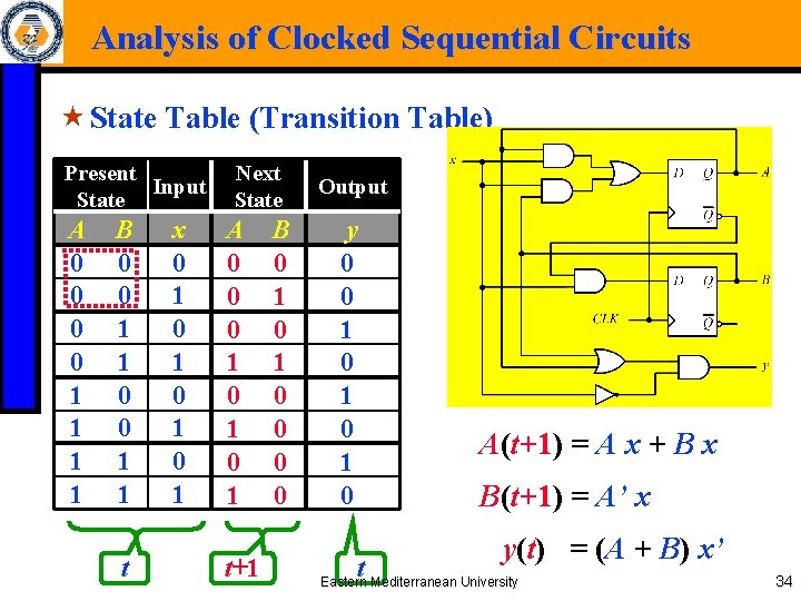
Analysis of Clocked Sequential Circuits « State Table (Transition Table) Present Input State A 0 0 1 1 B 0 0 1 1 t x 0 1 0 1 Next State A 0 0 0 1 0 1 t+1 B 0 1 0 0 Output y 0 0 1 0 1 0 t A(t+1) = A x + B x B(t+1) = A’ x y(t) = (A + B) x’ Eastern Mediterranean University 34

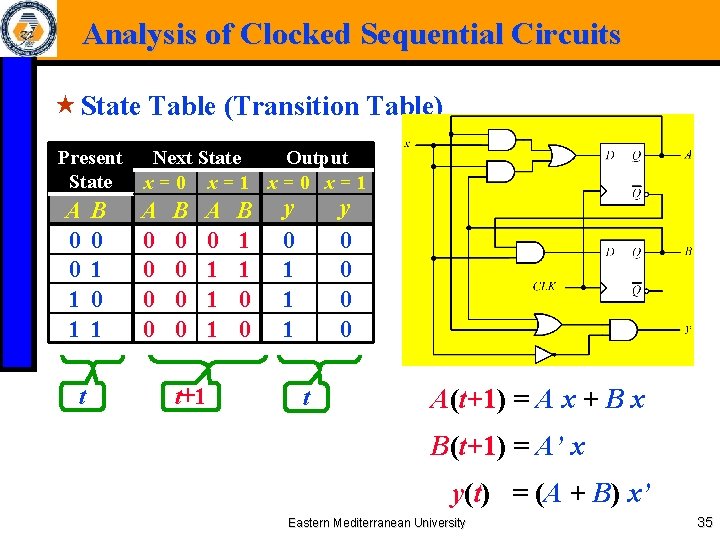
Analysis of Clocked Sequential Circuits « State Table (Transition Table) Present State A 0 0 1 1 t B 0 1 Next State Output x=0 x=1 A 0 0 B 0 0 A 0 1 1 1 t+1 B 1 1 0 0 y 0 1 1 1 y 0 0 t A(t+1) = A x + B x B(t+1) = A’ x y(t) = (A + B) x’ Eastern Mediterranean University 35

Analysis of Clocked Sequential Circuits « State Diagram Present State input/output AB 0/0 1/0 0/1 00 Next State x=0 Output x=1 x=0 x=1 A B A B y y 0 0 0 1 1 1 0 0 0 1 0 1 1 0 0 1 0 10 0/1 1/0 0/1 01 1/0 11 1/0 Eastern Mediterranean University 36

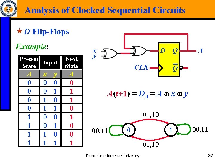
Analysis of Clocked Sequential Circuits « D Flip-Flops Example: Present Input State A 0 0 1 1 x 0 0 1 1 y 0 1 0 1 Next State A 0 1 1 0 0 1 x y D CLK Q A(t+1) = DA = A x y 01, 10 00, 11 0 1 00, 11 01, 10 Eastern Mediterranean University 37

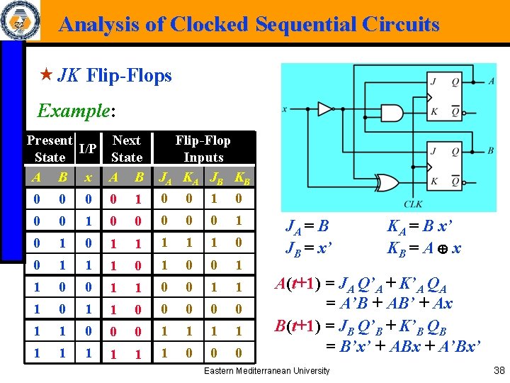
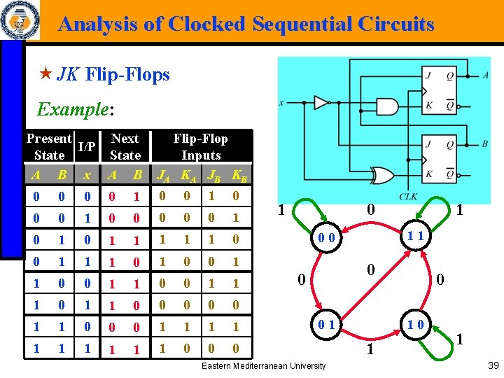
Analysis of Clocked Sequential Circuits « JK Flip-Flops Example: Present Next I/P State A B x A B Flip-Flop Inputs JA KA JB KB 0 0 1 0 0 0 1 0 1 1 1 0 0 1 1 0 0 1 1 1 0 0 0 1 1 1 1 1 0 0 0 JA = B JB = x’ KA = B x’ KB = A x A(t+1) = JA Q’A + K’A QA = A’B + AB’ + Ax B(t+1) = JB Q’B + K’B QB = B’x’ + ABx + A’Bx’ Eastern Mediterranean University 38

Analysis of Clocked Sequential Circuits « JK Flip-Flops Example: Present Next I/P State A B x A B Flip-Flop Inputs JA KA JB KB 0 0 1 0 0 0 1 0 1 1 1 0 0 1 1 0 0 1 1 1 0 0 0 1 1 1 1 1 0 0 0 1 11 00 0 0 01 Eastern Mediterranean University 0 10 1 1 39

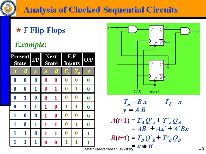
Analysis of Clocked Sequential Circuits « T Flip-Flops Example: Present Next F. F I/P O/P State Inputs A B x A B TA TB y 0 0 0 0 0 1 0 1 0 0 1 1 1 0 1 0 0 0 0 1 1 1 0 1 1 1 0 0 1 TA = B x y =AB TB = x A(t+1) = TA Q’A + T’A QA = AB’ + Ax’ + A’Bx 0 1 B(t+1) = TB Q’B + T’B QB 1 1 =x B Eastern Mediterranean University 40

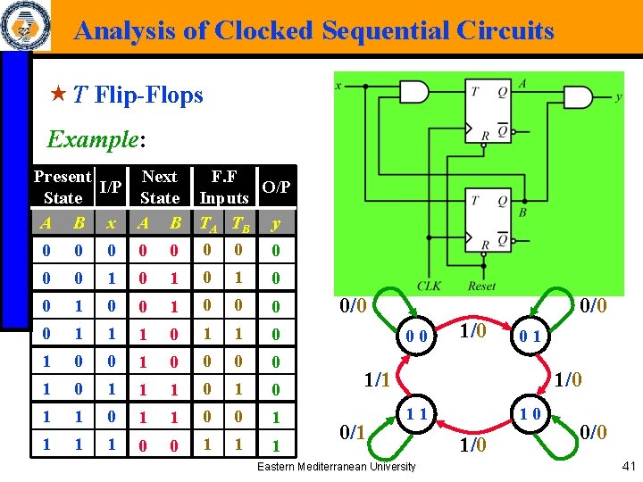
Analysis of Clocked Sequential Circuits « T Flip-Flops Example: Present Next F. F I/P O/P State Inputs A B x A B TA TB y 0 0 0 0 0 1 0 1 0 0 1 1 1 0 1 0 0 0 0 1 1 1 0 0 1 1 0 0 1 1 1 0/0 00 1/0 01 1/1 0/1 1/0 11 Eastern Mediterranean University 10 1/0 0/0 41

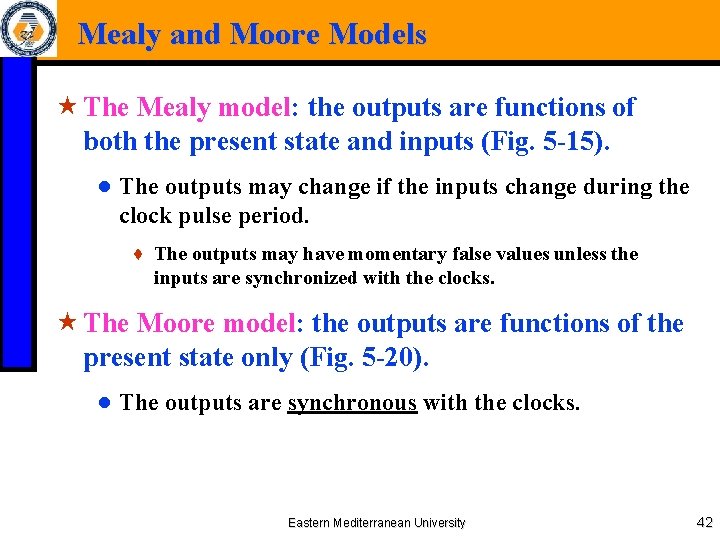
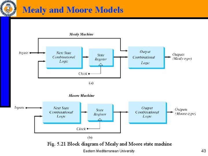
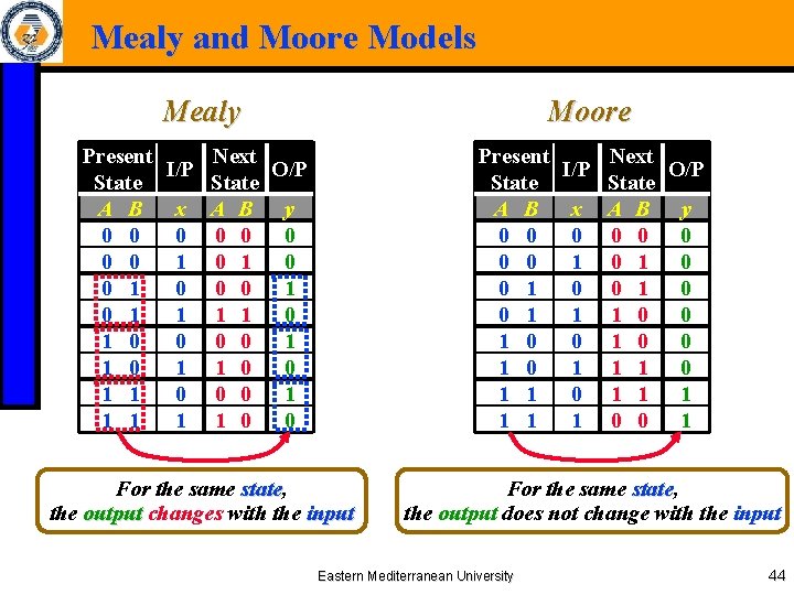
Mealy and Moore Models « The Mealy model: the outputs are functions of both the present state and inputs (Fig. 5 -15). ● The outputs may change if the inputs change during the clock pulse period. ♦ The outputs may have momentary false values unless the inputs are synchronized with the clocks. « The Moore model: the outputs are functions of the present state only (Fig. 5 -20). ● The outputs are synchronous with the clocks. Eastern Mediterranean University 42

Mealy and Moore Models Fig. 5. 21 Block diagram of Mealy and Moore state machine Eastern Mediterranean University 43

Mealy and Moore Models Mealy Present State A B 0 0 0 1 0 1 1 1 1 I/P x 0 1 0 1 Moore Next O/P State A B y 0 0 1 0 0 0 1 1 0 0 Present State A B 0 0 0 1 0 1 1 1 1 For the same state, state the output changes with the input I/P x 0 1 0 1 Next O/P State A B y 0 0 1 0 0 1 1 1 0 0 1 For the same state, state the output does not change with the input Eastern Mediterranean University 44

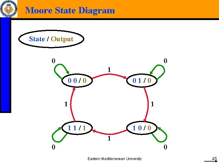
Moore State Diagram State / Output 0 0 1 00/0 01/0 1 1 11/1 10/0 1 0 0 Eastern Mediterranean University 45

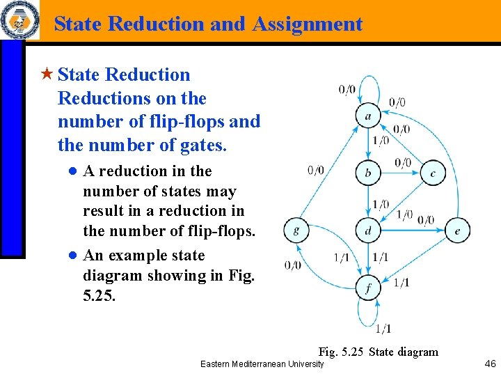
State Reduction and Assignment « State Reductions on the number of flip-flops and the number of gates. ● A reduction in the number of states may result in a reduction in the number of flip-flops. ● An example state diagram showing in Fig. 5. 25 State diagram Eastern Mediterranean University 46

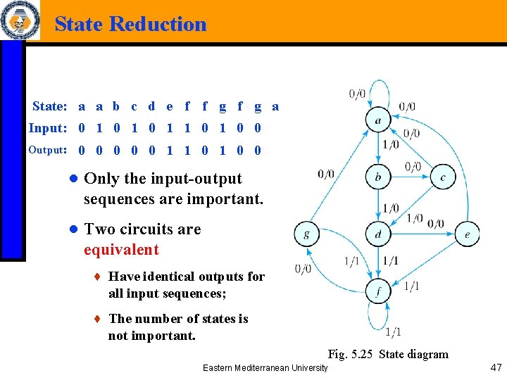
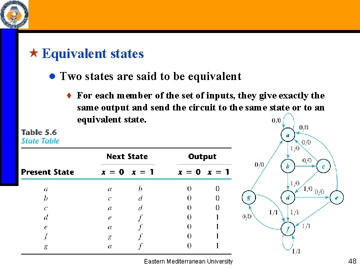
State Reduction State: a a b c d e f f g a Input: 0 1 0 1 1 0 0 Output: 0 0 0 1 1 0 0 ● Only the input-output sequences are important. ● Two circuits are equivalent ♦ Have identical outputs for all input sequences; ♦ The number of states is not important. Fig. 5. 25 State diagram Eastern Mediterranean University 47

« Equivalent states ● Two states are said to be equivalent ♦ For each member of the set of inputs, they give exactly the same output and send the circuit to the same state or to an equivalent state. ♦ One of them can be removed. Eastern Mediterranean University 48

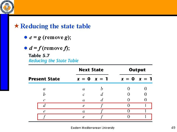
« Reducing the state table ● e = g (remove g); ● d = f (remove f); Eastern Mediterranean University 49

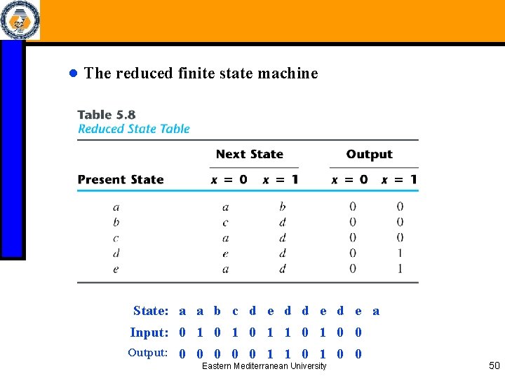
● The reduced finite state machine State: a a b c d e d e a Input: 0 1 0 1 1 0 0 Output: 0 0 0 1 1 0 0 Eastern Mediterranean University 50

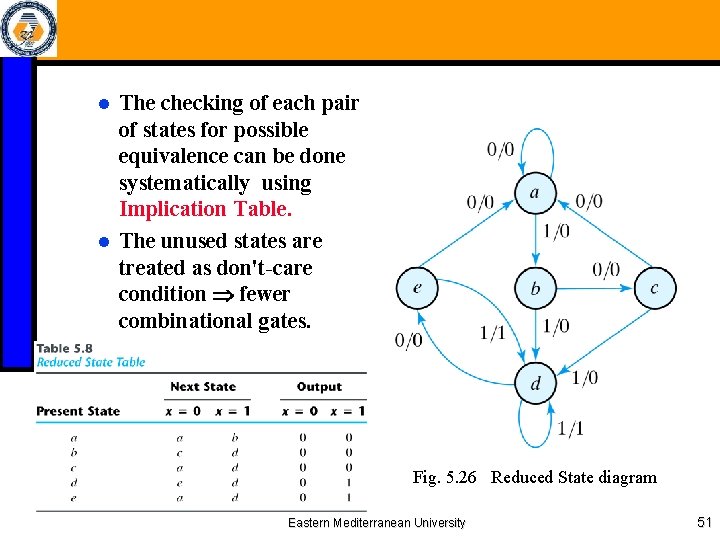
● The checking of each pair of states for possible equivalence can be done systematically using Implication Table. ● The unused states are treated as don't-care condition Þ fewer combinational gates. Fig. 5. 26 Reduced State diagram Eastern Mediterranean University 51

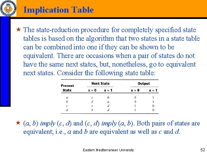
Implication Table « The state-reduction procedure for completely specified state tables is based on the algorithm that two states in a state table can be combined into one if they can be shown to be equivalent. There are occasions when a pair of states do not have the same next states, but, nonetheless, go to equivalent next states. Consider the following state table: « (a, b) imply (c, d) and (c, d) imply (a, b). Both pairs of states are equivalent; i. e. , a and b are equivalent as well as c and d. Eastern Mediterranean University 52

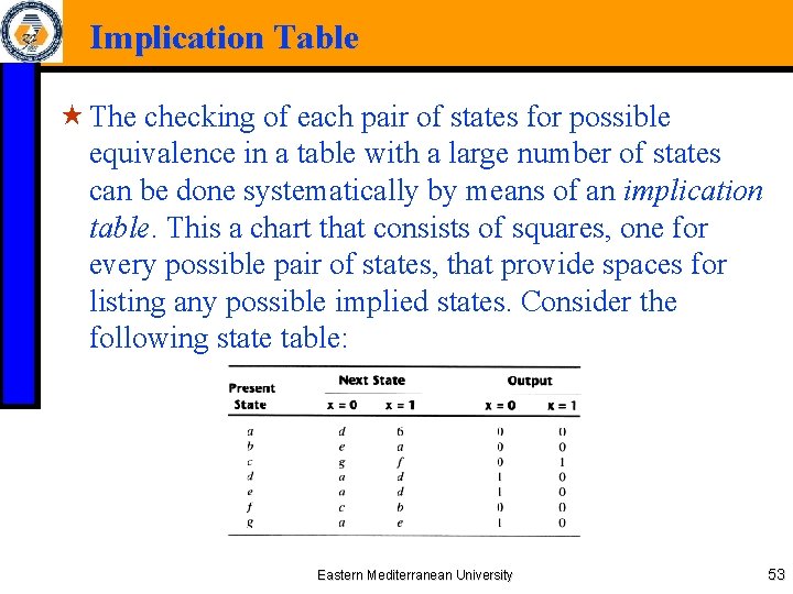
Implication Table « The checking of each pair of states for possible equivalence in a table with a large number of states can be done systematically by means of an implication table. This a chart that consists of squares, one for every possible pair of states, that provide spaces for listing any possible implied states. Consider the following state table: Eastern Mediterranean University 53

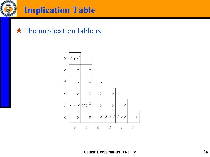
Implication Table « The implication table is: Eastern Mediterranean University 54

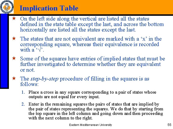
Implication Table « On the left side along the vertical are listed all the states defined in the state table except the last, and across the bottom horizontally are listed all the states except the last. « The states that are not equivalent are marked with a ‘x’ in the corresponding square, whereas their equivalence is recorded with a ‘√’. « Some of the squares have entries of implied states that must be further investigated to determine whether they are equivalent or not. « The step-by-step procedure of filling in the squares is as follows: 1. Place a cross in any square corresponding to a pair of states whose outputs are not equal for every input. 2. Enter in the remaining squares the pairs of states that are implied by the pair of states representing the squares. We do that by starting from the top square in the left column and going down and then proceeding with the next column to the right. Eastern Mediterranean University 55

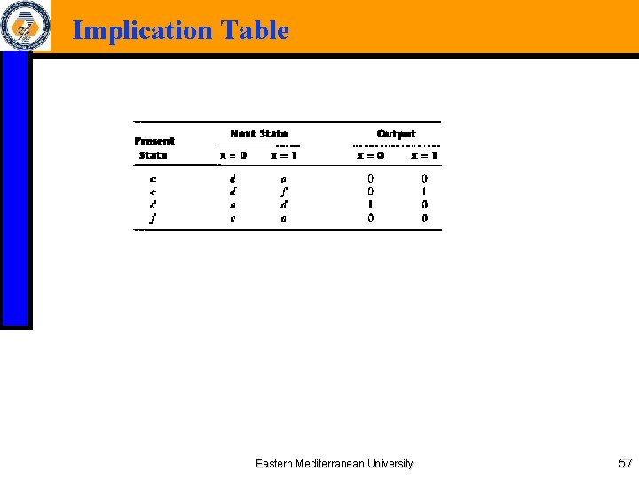
Implication Table 3. Make successive passes through the table to determine whether any additional squares should be marked with a ‘x’. A square in the table is crossed out if it contains at least one implied pair that is not equivalent. 4. Finally, all the squares that have no crosses are recorded with check marks. The equivalent states are: (a, b), (d, e), (d, g), (e, g). We now combine pairs of states into larger groups of equivalent states. The last three pairs can be combined into a set of three equivalent states (d, e, g) because each one of the states in the group is equivalent to the other two. The final partition of these states consists of the equivalent states found from the implication table, together with all the remaining states in the state table that are not equivalent to any other state: (a, b) (c) (d, e, g) (f) The reduced state table is: Eastern Mediterranean University 56

Implication Table Eastern Mediterranean University 57

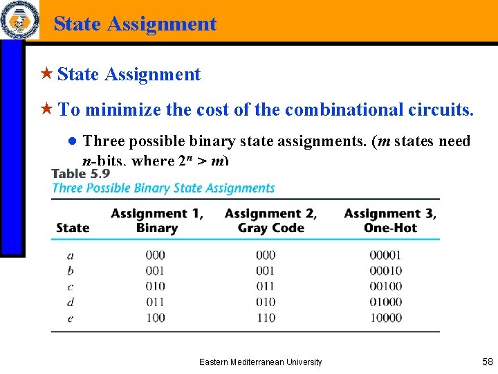
State Assignment « To minimize the cost of the combinational circuits. ● Three possible binary state assignments. (m states need n-bits, where 2 n > m) Eastern Mediterranean University 58

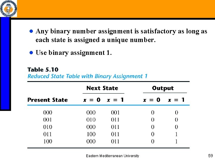
● Any binary number assignment is satisfactory as long as each state is assigned a unique number. ● Use binary assignment 1. Eastern Mediterranean University 59

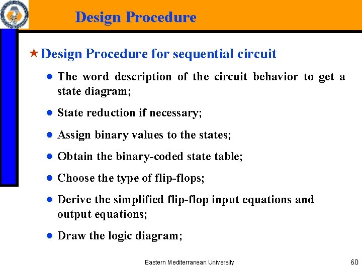
Design Procedure « Design Procedure for sequential circuit ● The word description of the circuit behavior to get a state diagram; ● State reduction if necessary; ● Assign binary values to the states; ● Obtain the binary-coded state table; ● Choose the type of flip-flops; ● Derive the simplified flip-flop input equations and output equations; ● Draw the logic diagram; Eastern Mediterranean University 60

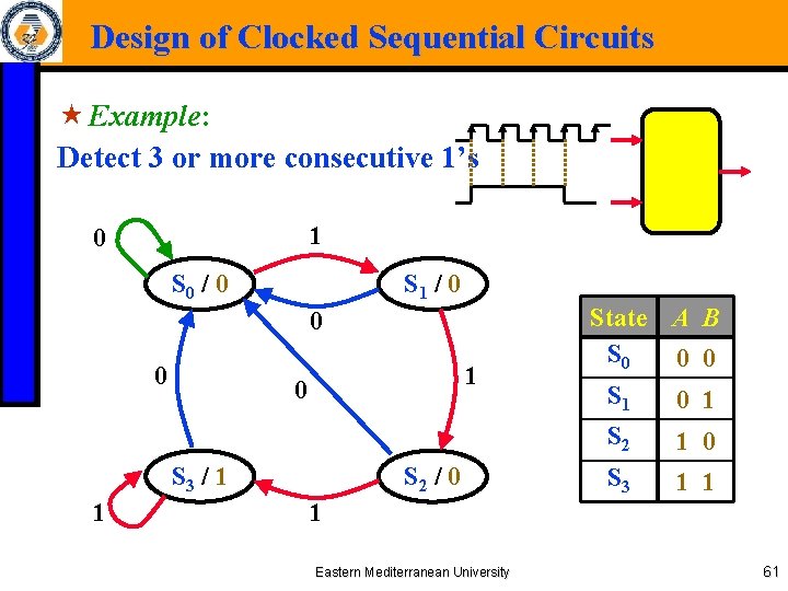
Design of Clocked Sequential Circuits « Example: Detect 3 or more consecutive 1’s 1 0 S 0 / 0 S 1 / 0 0 0 1 0 S 3 / 1 1 S 2 / 0 State A B S 0 0 0 S 1 0 1 S 2 1 0 S 3 1 1 1 Eastern Mediterranean University 61

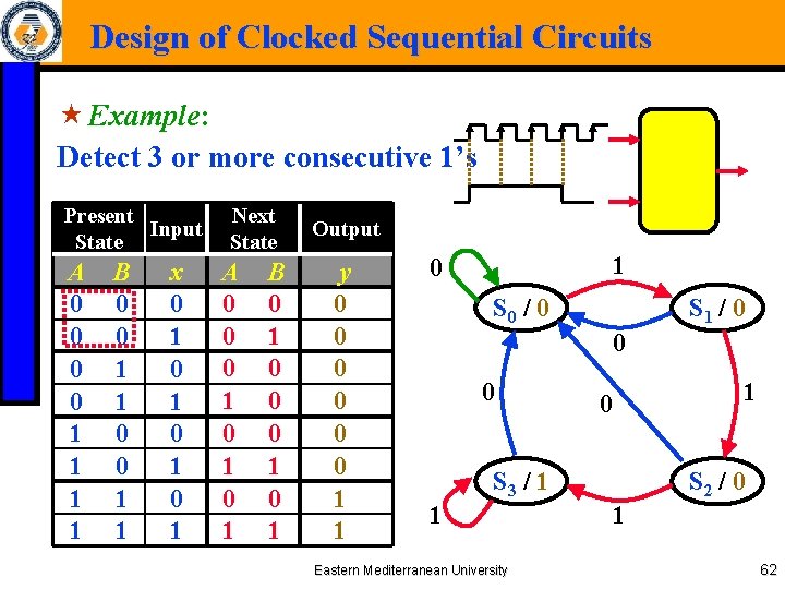
Design of Clocked Sequential Circuits « Example: Detect 3 or more consecutive 1’s Present Input State A 0 0 1 1 B 0 0 1 1 x 0 1 0 1 Next State A 0 0 0 1 0 1 B 0 1 0 0 0 1 Output y 0 0 0 1 1 1 0 S 0 / 0 S 1 / 0 0 S 3 / 1 1 Eastern Mediterranean University 1 S 2 / 0 1 62

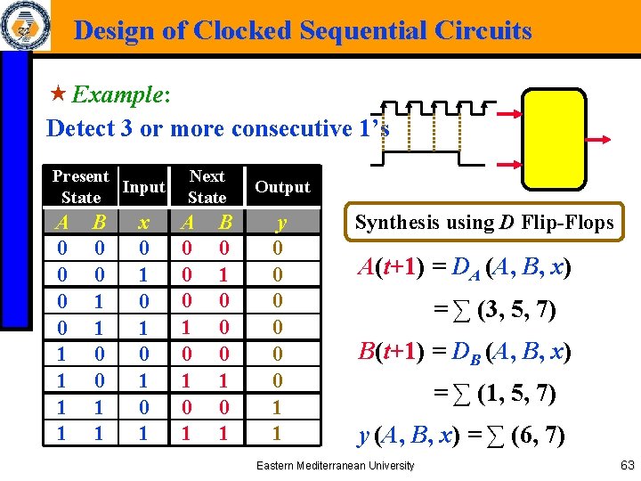
Design of Clocked Sequential Circuits « Example: Detect 3 or more consecutive 1’s Present Input State A 0 0 1 1 B 0 0 1 1 x 0 1 0 1 Next State A 0 0 0 1 0 1 B 0 1 0 0 0 1 Output y 0 0 0 1 1 Synthesis using D Flip-Flops A(t+1) = DA (A, B, x) = ∑ (3, 5, 7) B(t+1) = DB (A, B, x) = ∑ (1, 5, 7) y (A, B, x) = ∑ (6, 7) Eastern Mediterranean University 63

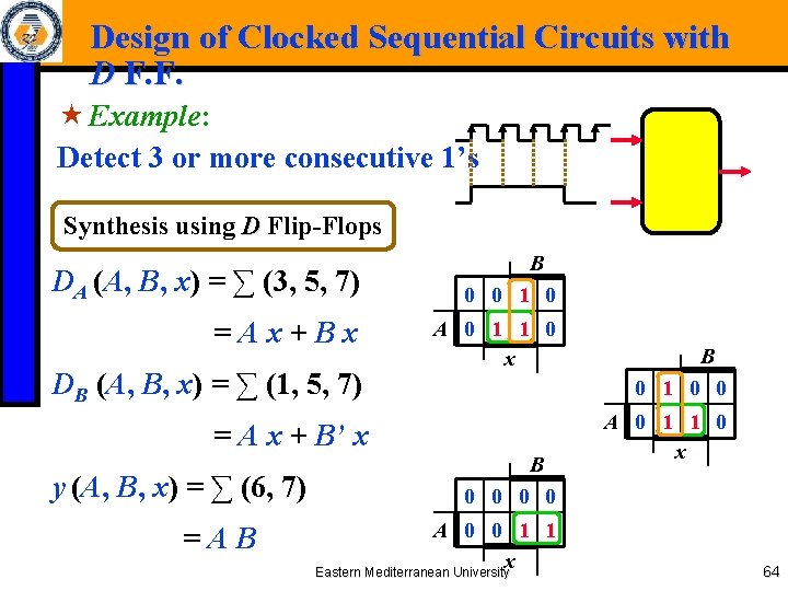
Design of Clocked Sequential Circuits with D F. F. « Example: Detect 3 or more consecutive 1’s Synthesis using D Flip-Flops DA (A, B, x) = ∑ (3, 5, 7) =Ax+Bx DB (A, B, x) = ∑ (1, 5, 7) B 0 0 1 0 A 0 1 1 0 x 0 1 0 0 = A x + B’ x y (A, B, x) = ∑ (6, 7) =AB B B A 0 1 1 0 x 0 0 A 0 0 1 1 x Eastern Mediterranean University 64

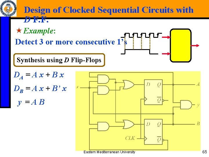
Design of Clocked Sequential Circuits with D F. F. « Example: Detect 3 or more consecutive 1’s Synthesis using D Flip-Flops DA = A x + B x DB = A x + B’ x y =AB Eastern Mediterranean University 65

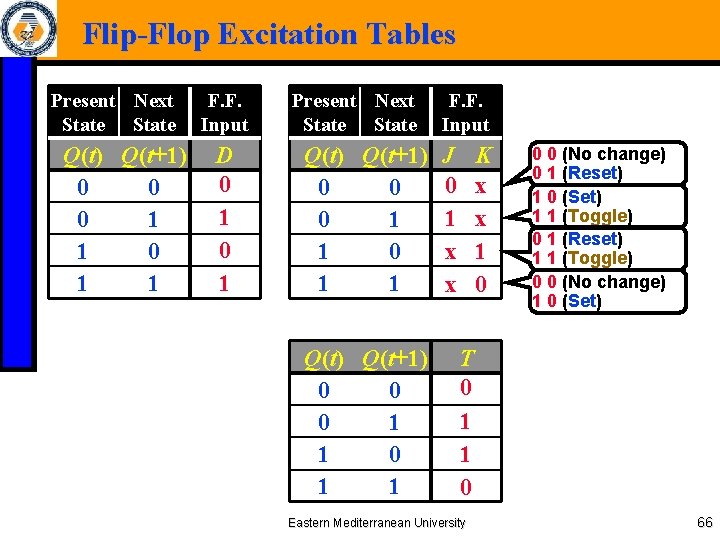
Flip-Flop Excitation Tables Present Next State Q(t) Q(t+1) 0 0 0 1 1 F. F. Input D 0 1 Present Next State F. F. Input Q(t) Q(t+1) J K 0 x 0 0 1 x 0 1 1 0 x 1 1 1 x 0 Q(t) Q(t+1) 0 0 0 1 1 0 0 (No change) 0 1 (Reset) 1 0 (Set) 1 1 (Toggle) 0 1 (Reset) 1 1 (Toggle) 0 0 (No change) 1 0 (Set) T 0 1 1 0 Eastern Mediterranean University 66

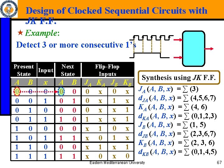
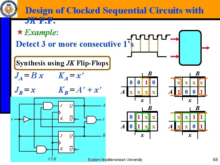
Design of Clocked Sequential Circuits with JK F. F. « Example: Detect 3 or more consecutive 1’s Present Input State A 0 0 1 1 B 0 0 1 1 x 0 1 0 1 Next State A 0 0 0 1 0 1 Flip-Flop Inputs B JA 0 0 1 0 x 1 x KA x x 1 0 JB KB 0 x 1 x 1 0 x 1 x 0 Synthesis using JK F. F. JA (A, B, x) = ∑ (3) d. JA (A, B, x) = ∑ (4, 5, 6, 7) KA (A, B, x) = ∑ (4, 6) d. KA (A, B, x) = ∑ (0, 1, 2, 3) JB (A, B, x) = ∑ (1, 5) d. JB (A, B, x) = ∑ (2, 3, 6, 7) KB (A, B, x) = ∑ (2, 3, 6) d. KB (A, B, x) = ∑ (0, 1, 4, 5) Eastern Mediterranean University 67

Design of Clocked Sequential Circuits with JK F. F. « Example: Detect 3 or more consecutive 1’s Synthesis using JK Flip-Flops B JA = B x KA = x’ JB = x KB = A’ + x’ B 0 0 1 0 x x A x x x B 0 1 x x A 1 0 0 1 x B x x 1 1 A 0 1 x x x A x x 0 1 x Eastern Mediterranean University 68

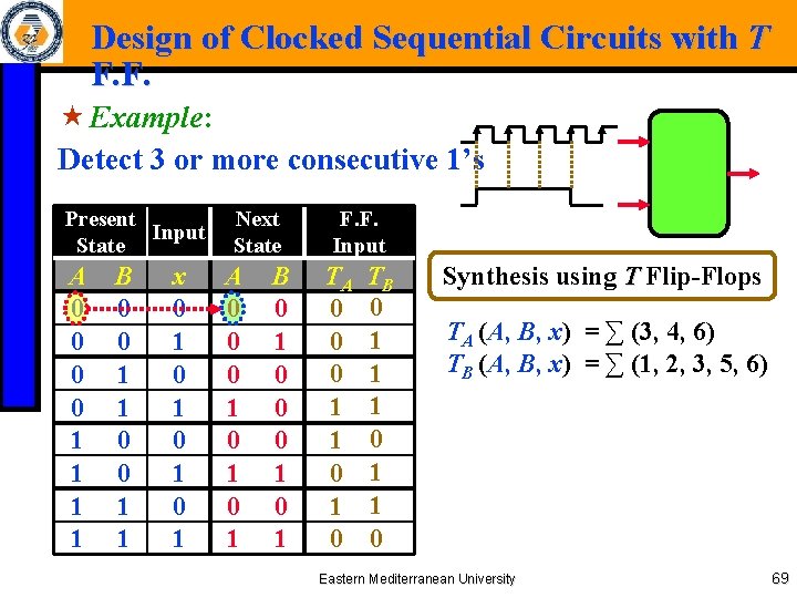
Design of Clocked Sequential Circuits with T F. F. « Example: Detect 3 or more consecutive 1’s Present Input State A 0 0 1 1 B 0 0 1 1 x 0 1 0 1 Next State A 0 0 0 1 0 1 B 0 1 0 0 0 1 F. F. Input TA 0 0 0 1 1 0 TB 0 1 1 1 0 Synthesis using T Flip-Flops TA (A, B, x) = ∑ (3, 4, 6) TB (A, B, x) = ∑ (1, 2, 3, 5, 6) Eastern Mediterranean University 69

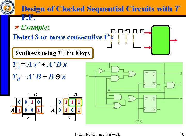
Design of Clocked Sequential Circuits with T F. F. « Example: Detect 3 or more consecutive 1’s Synthesis using T Flip-Flops TA = A x’ + A’ B x TB = A’ B + B x B B 0 0 1 1 1 A 1 0 0 1 x A 0 1 x Eastern Mediterranean University 70