Digital Logic Design Dr Waseem Ikram Lecture No


- Slides: 20

Digital Logic & Design Dr. Waseem Ikram Lecture No. 43

Recap n FLASH Structure n n n Common Drain lines Common Source lines (column select lines) Row select activates all cells Current flows through common drain line to active load Voltage drop across active load compared with reference voltage High output indicates 0 stored and vice versa

Recap FIFO Memory n n n n Connecting two devices communicating at different data rates Direct connection Connection through buffer Buffer contents writing/reading Keyboard buffer FIFO Implementation using shift registers FIFO Implementation using Memory

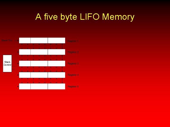
A five byte LIFO Memory

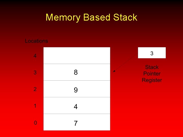
Memory Based Stack

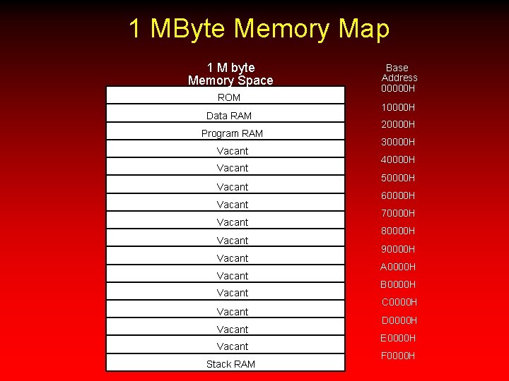
1 MByte Memory Map 1 M byte Memory Space ROM Data RAM Program RAM Vacant Vacant Vacant Stack RAM Base Address 00000 H 10000 H 20000 H 30000 H 40000 H 50000 H 60000 H 70000 H 80000 H 90000 H A 0000 H B 0000 H C 0000 H D 0000 H E 0000 H F 0000 H

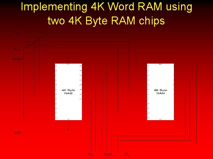
Implementing 4 K Word RAM using two 4 K Byte RAM chips

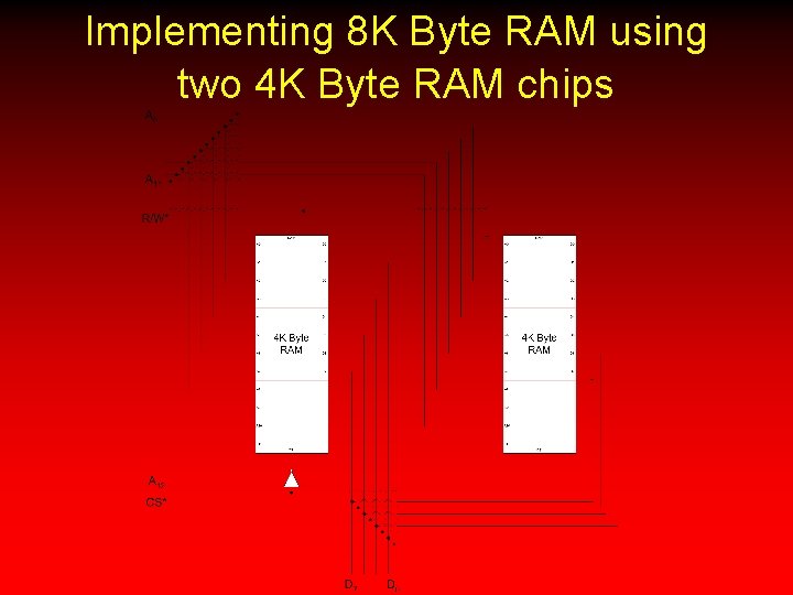
Implementing 8 K Byte RAM using two 4 K Byte RAM chips

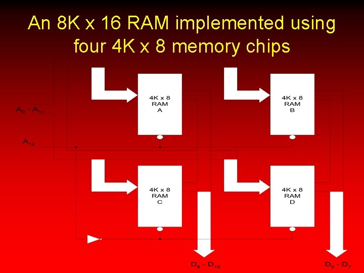
An 8 K x 16 RAM implemented using four 4 K x 8 memory chips

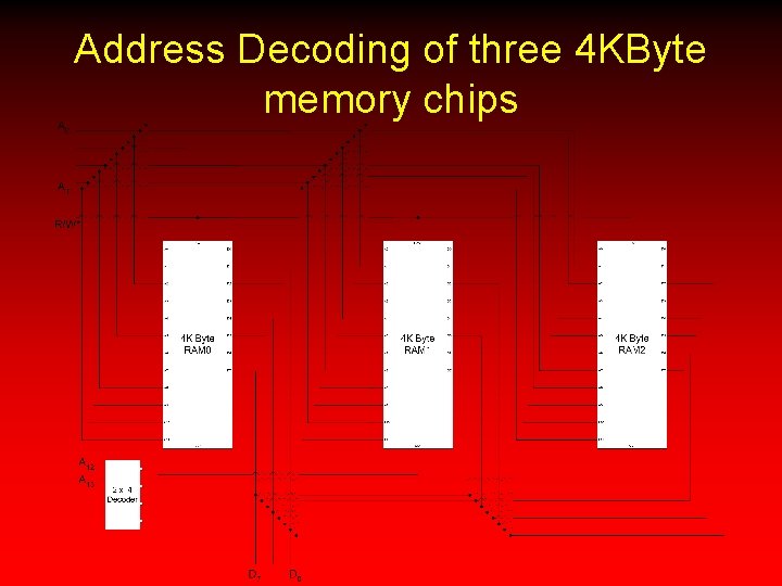
Address Decoding of three 4 KByte memory chips

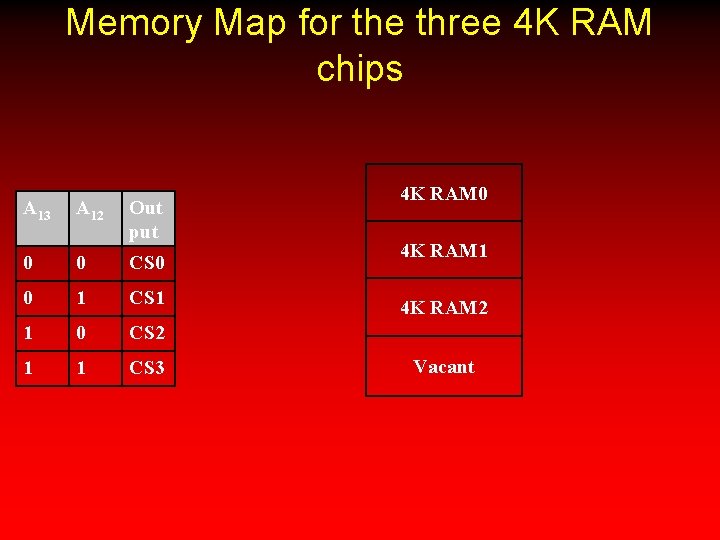
Memory Map for the three 4 K RAM chips A 13 A 12 Out put 0 0 CS 0 0 1 CS 1 1 0 CS 2 1 1 CS 3 4 K RAM 0 4 K RAM 1 4 K RAM 2 Vacant

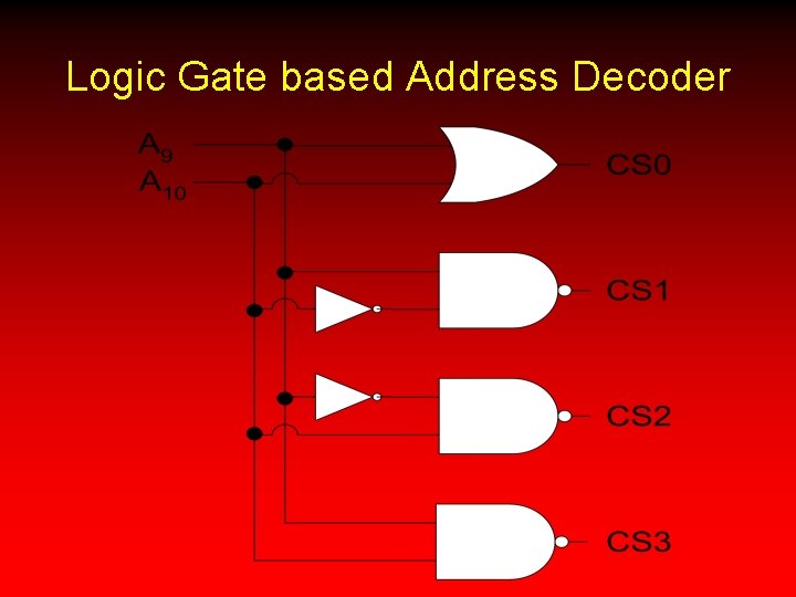
Logic Gate based Address Decoder

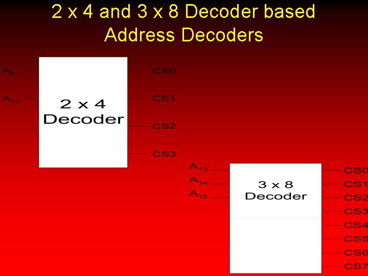
2 x 4 and 3 x 8 Decoder based Address Decoders

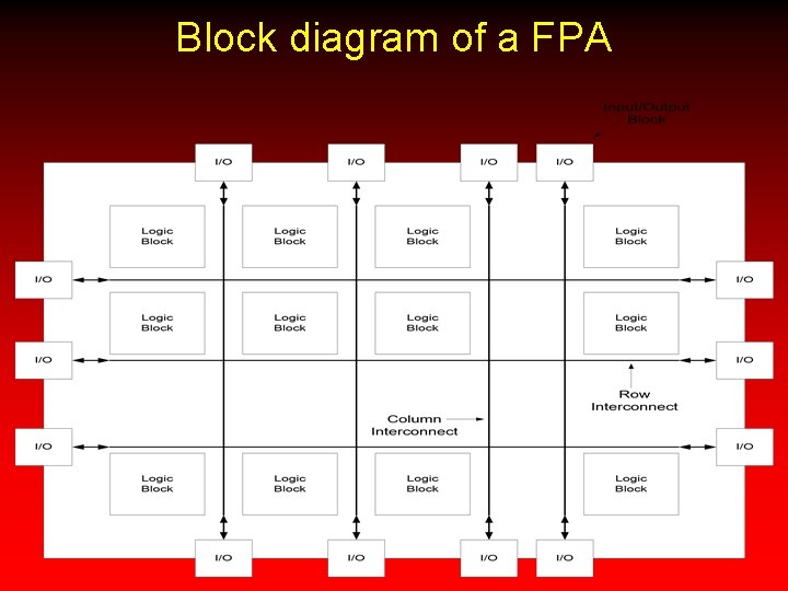
Block diagram of a FPA


LIFO Memory n n n Use of Stack in Computer systems Implementing LIFO using parallel In and parallel out shift registers (fig 1) Implementing Stack using Memory (fig 2)

Memory Expansion n n Memory Requirement is large Memory Implemented small n n Standard data unit size Standard number of memory locations Base address of memory Map fig (3) n n 1 MB memory map Divided into 16, 64 K blocks ROM, Data, Program, Stack 12, 64 K vacant blocks for expansion

Memory Expansion n n Expanding Data Unit size (fig 4) Expanding Locations (fig 5) Expanding Data unit size and locations (fig 6) Address Decoders n n n Accessing memory at specified base address (fig 7) Logic gate decoders (fig 8) n x m gate decoders (fig 9)

FPGAs Field Programmable Logic Array (fig 10) n Logic blocks n n n Generate logic functions by programming LUT Row & Col programmable interconnects I/O programmable blocks