Digital Logic Design Dr Waseem Ikram Lecture 45
- Slides: 26

Digital Logic & Design Dr. Waseem Ikram Lecture 45

Recap Logic Block n Multiple Logic Elements n LUT, flip-flop, cascade logic n Control logic, programmable selects

Recap Implementing function by Programming LUT n Example 1 n Example 2 full adder Programming Row & Column interconnects through transistor switches.

Recap Conversion of real world quantities n Mobile phones n Digital Thermometers n Digital storage of sound and pictures n Digital voltmeters n Industrial control and monitoring.

Recap Sampling n Under-sampling n Over-sampling n Sampling frequency n Nyquist frequency Holding Sampled value n Sample and Hold Circuit

Recap Quantization n Process of converting analogue value to a code n Few bits, quantization levels less accurate n More bits, quantization levels more accurate

Recap Linear Amplifier n Inverting/Non-inverting inputs n Single outputs n High input impedance n Low output impedance n Very High voltage gain n Inverting Amplifier n Comparator

Recap FLASH Converter n Fast conversion time n Expensive circuit complexity n Resistor voltage divider n Multiple Op-Amps as comparators n Input signal connected to all comparators n Comparator o/p high if i/p higher than ref n Priority encoder n Encoder o/p is digital equivalent of i/p

Recap DUAL-SLOPE A/D Converter n Slower than FLASH n Used in Digital voltmeters and other measuring instruments n Ckt. Diagram n Working

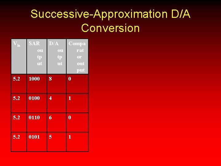
Successive Approximation Converter n n Widely used Faster conversion time w. r. t. dual slope Explain operation Circuit diagram (fig 1)

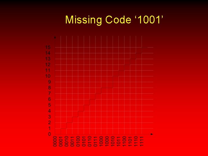
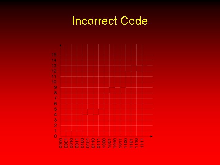
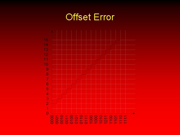
A/D Converter Errors n n n Missing Code (fig 14. 26 a) Incorrect Code (fig 14. 26 b) Offset (fig 14. 26 c)

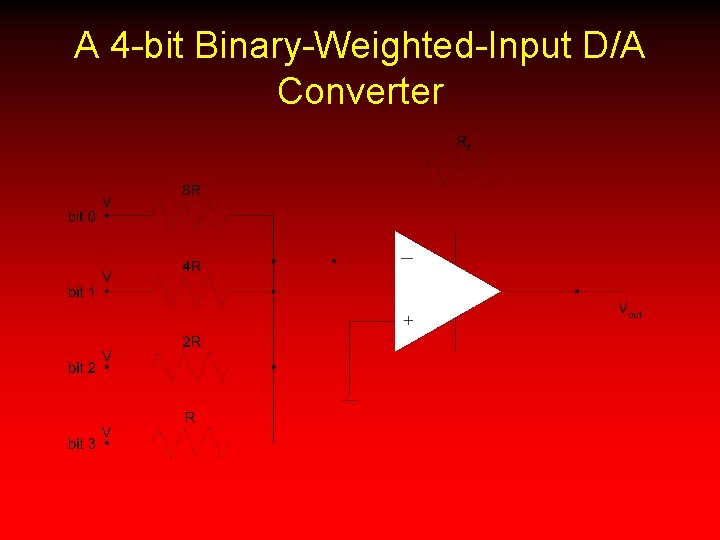
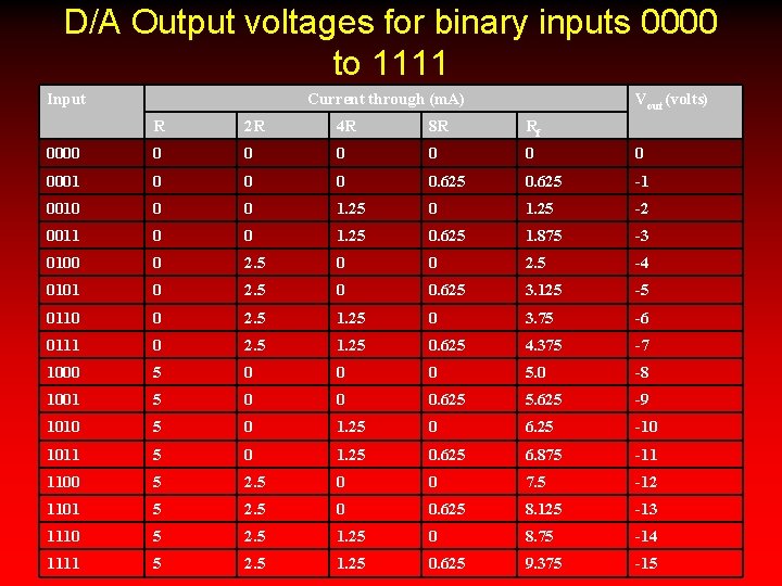
Binary-Weighted-Input D/A Converter n n Summer Weighted Resistors Circuit (fig 3, tab 2) Disadvantage n Weighted resistors of exact value

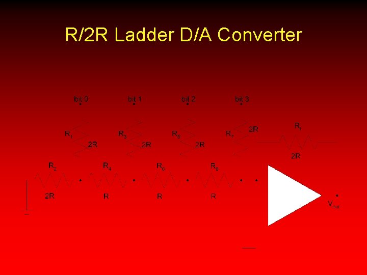
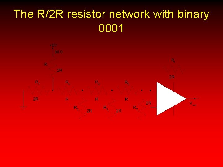
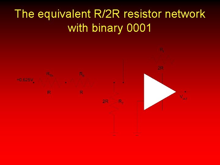
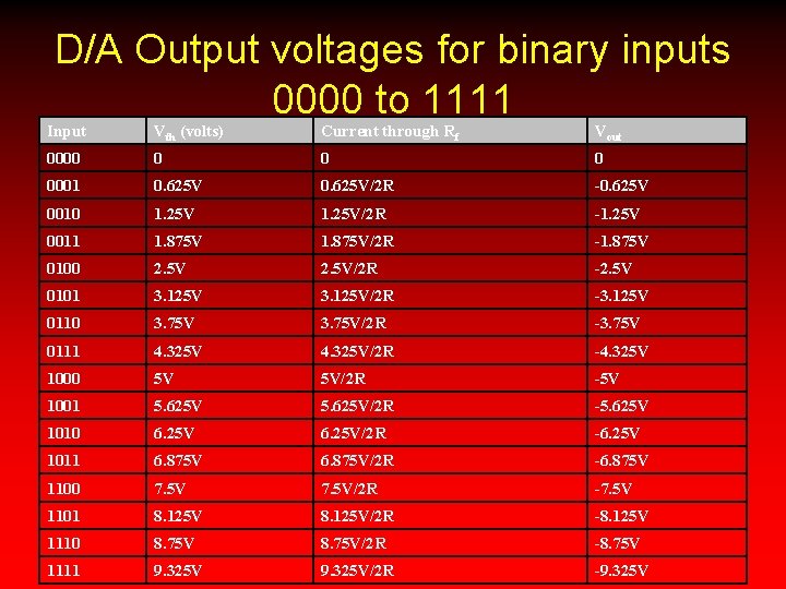
R/2 R Ladder D/A Converter n n n Circuit (fig 4) Equivalent circuit (fig 5 a) Simplified circuit (fig 5 b, table 3)

Performance Characteristics of D/A Converters n n Resolution n Number of bits that are converted n Reciprocal of the number of discrete steps in the output expressed in percentage n 4 -bit D/A has a resolution of 6. 67% (1/15 x 100) Accuracy n Actual o/p of a D/A w. r. t. expected o/p n Expressed as a percentage of full-scale o/p n O/p = 10 v accuracy is 0. 1% then max error is 10 m. V n Should not be +/-1/2 least sign. bit

Performance Characteristics of D/A Converters n n n Linearity n Deviation form the straight line output of a D/A Monotonicity n DAC does not take any reverse steps when D/A sequenced over its entire range of input steps Settling time n The time it takes the D/A to settle within +/- ½ LSB of its final value when a change occurs in its input

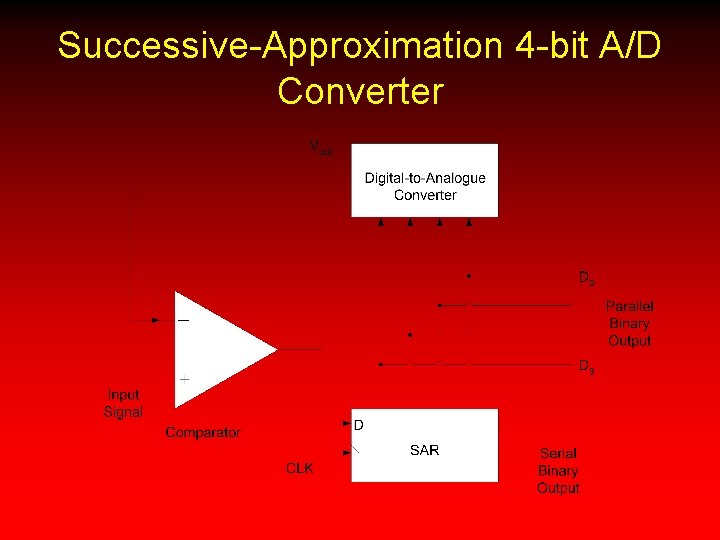
Successive-Approximation 4 -bit A/D Converter

Successive-Approximation D/A Conversion Vin SAR ou tp ut D/A Compa ou rat tp or ut out put 5. 2 1000 8 0 5. 2 0100 4 1 5. 2 0110 6 0 5. 2 0101 5 1

Missing Code ‘ 1001’

Incorrect Code

Offset Error

A 4 -bit Binary-Weighted-Input D/A Converter

D/A Output voltages for binary inputs 0000 to 1111 Input Current through (m. A) Vout (volts) R 2 R 4 R 8 R Rf 0000 0 0 0 0001 0 0. 625 -1 0010 0 0 1. 25 -2 0011 0 0 1. 25 0. 625 1. 875 -3 0100 0 2. 5 -4 0101 0 2. 5 0 0. 625 3. 125 -5 0110 0 2. 5 1. 25 0 3. 75 -6 0111 0 2. 5 1. 25 0. 625 4. 375 -7 1000 5 0 0 0 5. 0 -8 1001 5 0 0 0. 625 5. 625 -9 1010 5 0 1. 25 0 6. 25 -10 1011 5 0 1. 25 0. 625 6. 875 -11 1100 5 2. 5 0 0 7. 5 -12 1101 5 2. 5 0 0. 625 8. 125 -13 1110 5 2. 5 1. 25 0 8. 75 -14 1111 5 2. 5 1. 25 0. 625 9. 375 -15

R/2 R Ladder D/A Converter

The R/2 R resistor network with binary 0001

The equivalent R/2 R resistor network with binary 0001

D/A Output voltages for binary inputs 0000 to 1111 Input Vth (volts) Current through Rf Vout 0000 0 0001 0. 625 V/2 R -0. 625 V 0010 1. 25 V/2 R -1. 25 V 0011 1. 875 V/2 R -1. 875 V 0100 2. 5 V/2 R -2. 5 V 0101 3. 125 V/2 R -3. 125 V 0110 3. 75 V/2 R -3. 75 V 0111 4. 325 V/2 R -4. 325 V 1000 5 V 5 V/2 R -5 V 1001 5. 625 V/2 R -5. 625 V 1010 6. 25 V/2 R -6. 25 V 1011 6. 875 V/2 R -6. 875 V 1100 7. 5 V/2 R -7. 5 V 1101 8. 125 V/2 R -8. 125 V 1110 8. 75 V/2 R -8. 75 V 1111 9. 325 V/2 R -9. 325 V