Digital IC Design Flow A quick look Prelayout










![Parameterized Design • module vector_and(z, a, b); parameter cardinality = 1; input [cardinality-1: 0] Parameterized Design • module vector_and(z, a, b); parameter cardinality = 1; input [cardinality-1: 0]](https://slidetodoc.com/presentation_image_h2/97005fef38ac1b69353d041a59e0ef9b/image-51.jpg)

![module fsm_car_speed_2(clk, keys, brake, accelerate, speed); input clk, keys, brake, accelerate; output [1: 0] module fsm_car_speed_2(clk, keys, brake, accelerate, speed); input clk, keys, brake, accelerate; output [1: 0]](https://slidetodoc.com/presentation_image_h2/97005fef38ac1b69353d041a59e0ef9b/image-61.jpg)

- Slides: 62

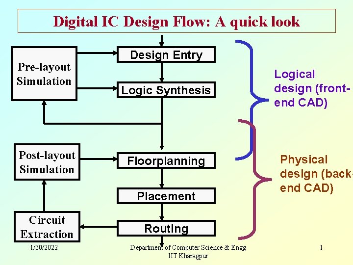
Digital IC Design Flow: A quick look Pre-layout Simulation Post-layout Simulation Design Entry Logic Synthesis Floorplanning Placement Circuit Extraction 1/30/2022 Logical design (frontend CAD) Physical design (backend CAD) Routing Department of Computer Science & Engg IIT Kharagpur 1

Design Methodology 1/30/2022 Department of Computer Science & Engg IIT Kharagpur 2

VLSI Design Styles • Programmable Logic Devices • Standard Cell Based Design • Full Custom Design 1/30/2022 Department of Computer Science & Engg IIT Kharagpur 3

Programmable Logic Devices 1/30/2022 Department of Computer Science & Engg IIT Kharagpur 4

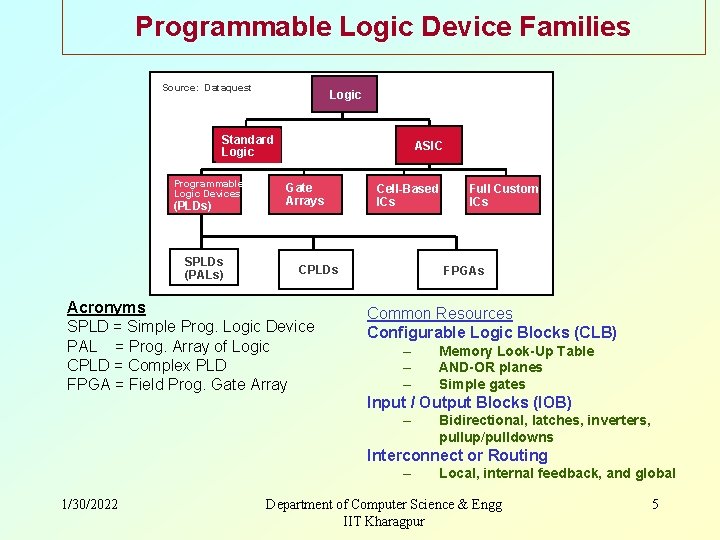
Programmable Logic Device Families Source: Dataquest Logic Standard Logic Programmable Logic Devices (PLDs) SPLDs (PALs) ASIC Gate Arrays Cell-Based ICs CPLDs Acronyms SPLD = Simple Prog. Logic Device PAL = Prog. Array of Logic CPLD = Complex PLD FPGA = Field Prog. Gate Array Full Custom ICs FPGAs Common Resources Configurable Logic Blocks (CLB) – – – Memory Look-Up Table AND-OR planes Simple gates Input / Output Blocks (IOB) – Bidirectional, latches, inverters, pullup/pulldowns Interconnect or Routing – 1/30/2022 Local, internal feedback, and global Department of Computer Science & Engg IIT Kharagpur 5

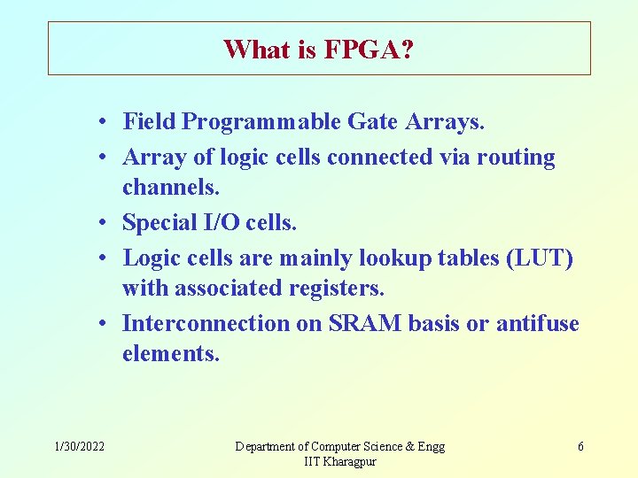
What is FPGA? • Field Programmable Gate Arrays. • Array of logic cells connected via routing channels. • Special I/O cells. • Logic cells are mainly lookup tables (LUT) with associated registers. • Interconnection on SRAM basis or antifuse elements. 1/30/2022 Department of Computer Science & Engg IIT Kharagpur 6

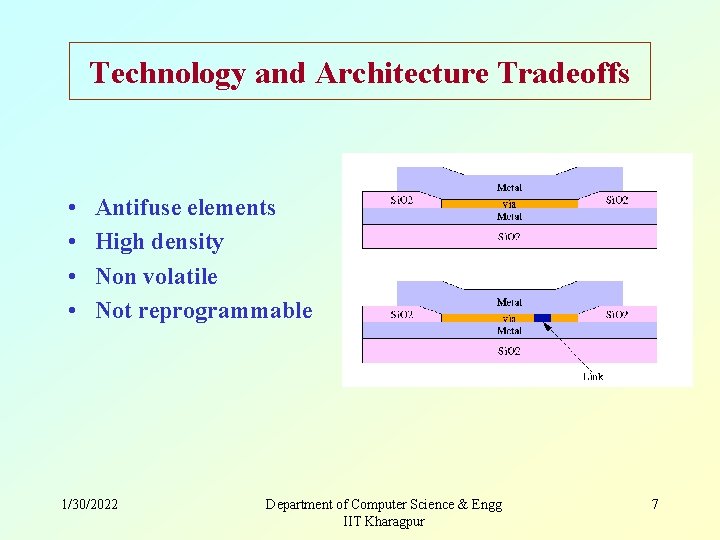
Technology and Architecture Tradeoffs • • Antifuse elements High density Non volatile Not reprogrammable 1/30/2022 Department of Computer Science & Engg IIT Kharagpur 7

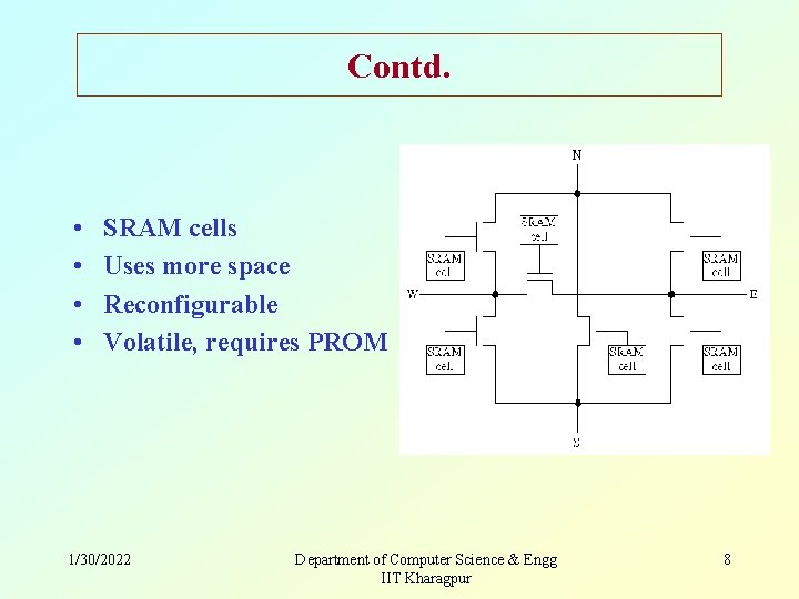
Contd. • • SRAM cells Uses more space Reconfigurable Volatile, requires PROM 1/30/2022 Department of Computer Science & Engg IIT Kharagpur 8

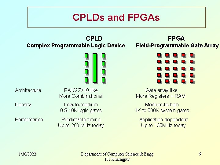
CPLDs and FPGAs CPLD Complex Programmable Logic Device FPGA Field-Programmable Gate Array Architecture PAL/22 V 10 -like More Combinational Gate array-like More Registers + RAM Density Low-to-medium 0. 5 -10 K logic gates Medium-to-high 1 K to 500 K system gates Predictable timing Up to 200 MHz today Application dependent Up to 135 MHz today Performance 1/30/2022 Department of Computer Science & Engg IIT Kharagpur 9

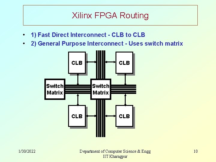
Xilinx FPGA Routing • 1) Fast Direct Interconnect - CLB to CLB • 2) General Purpose Interconnect - Uses switch matrix CLB Switch Matrix CLB 1/30/2022 CLB Department of Computer Science & Engg IIT Kharagpur 10

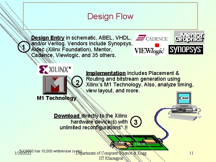
Design Flow 1 Design Entry in schematic, ABEL, VHDL, and/or Verilog. Vendors include Synopsys, Aldec (Xilinx Foundation), Mentor, Cadence, Viewlogic, and 35 others. 2 Implementation includes Placement & Routing and bitstream generation using Xilinx’s M 1 Technology. Also, analyze timing, view layout, and more. M 1 Technology Download directly to the Xilinx hardware device(s) with unlimited reconfigurations* !! XC 4000 *XC 9500 has 10, 000 write/erase cycles 1/30/2022 3 XC 4000 Department of Computer Science & Engg IIT Kharagpur 11

Altera FPGA Family • Altera Flex 10 K/10 KE – LEs (Logic elements) have 4 -input LUTS (look-up tables) +1 FF. – Fast Carry Chain between LE’s, cascade chain for logic operations. – Large blocks of SRAM available as well. • Altera Max 7000/Max 7000 A – EEPROM based, very fast (Tpd = 7. 5 ns). – Basically a PLD architecture with programmable interconnects. 1/30/2022 Department of Computer Science & Engg IIT Kharagpur 12

Gate Array 1/30/2022 Department of Computer Science & Engg IIT Kharagpur 13

Standard Cell Based Design 1/30/2022 Department of Computer Science & Engg IIT Kharagpur 14

Introduction • One of the most prevalent custom design styles. – Also called semi-custom design style. – Requires development of a full custom mask set. • Basic idea: – All of the commonly used logic cells are developed, characterized, and stored in a standard cell library. – A typical library may contain a few hundred cells including inverters, NAND gates, NOR gates, complex AOI, OAI gates, D-latches, and flip-flops. 1/30/2022 Department of Computer Science & Engg IIT Kharagpur 15

Contd. – Each gate type can have multiple implementations to provide adequate driving capability for different fanouts. • For instance, the inverter can have – standard size transistors, – double size transistors, and – quadruple size transistors • The chip designer can choose the proper size to achieve high circuit speed and layout density. 1/30/2022 Department of Computer Science & Engg IIT Kharagpur 16

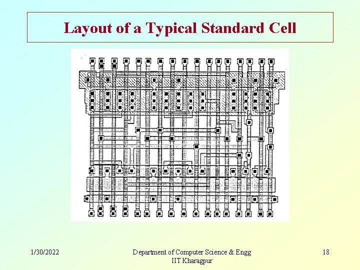
Characteristic of the Cells • Each cell is designed with a fixed height. – To enable automated placement of the cells, and – Routing of inter-cell connections. – A number of cells can be abutted side-by-side to form rows. • The power and ground rails typically run parallel to the upper and lower boundaries of the cell. – Neighboring cells share a common power and ground bus. – n. MOS transistors are located closer to the ground rail while the p. MOS transistors are placed closer to the power rail. • The input and output pins are located on the upper and lower boundaries of the cell. 1/30/2022 Department of Computer Science & Engg IIT Kharagpur 17

Layout of a Typical Standard Cell 1/30/2022 Department of Computer Science & Engg IIT Kharagpur 18

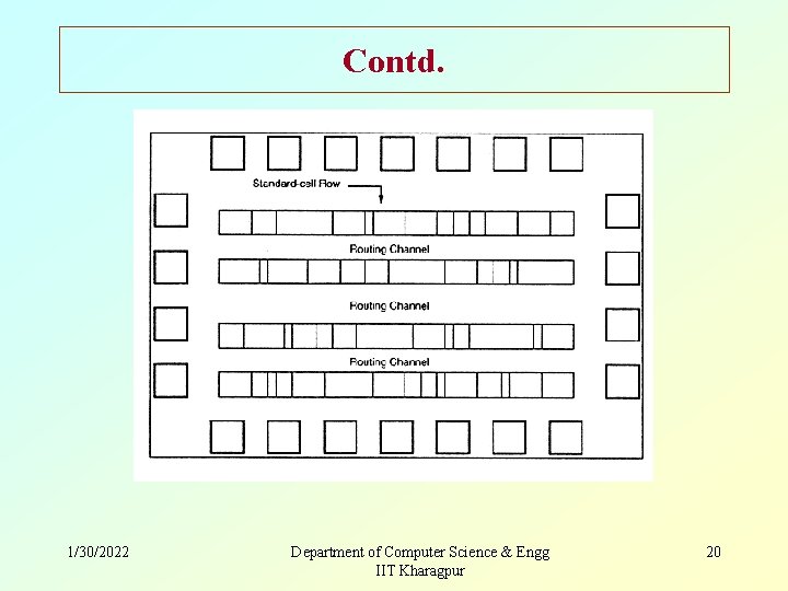
Floorplan for Standard Cell Design • Inside the I/O frame which is reserved for I/O cells, the chip area contains rows or columns of standard cells. – Between cell rows are channels for dedicated intercell routing. – Over-the-cell routing is also possible. • The physical design and layout of logic cells ensure that – When placed into rows, their heights match. – Neighboring cells can be abutted side-by-side, which provides natural connections for power and ground lines in each row. 1/30/2022 Department of Computer Science & Engg IIT Kharagpur 19

Contd. 1/30/2022 Department of Computer Science & Engg IIT Kharagpur 20

Contd. • After chip logic design is done using standard cells in the library: – The most challenging task is to place individual cells into rows. – Interconnect them in a way that meets stringent design goals in • circuit speed, • chip area, and • power consumption. – Many advanced CAD tools for place-and-route have been developed and used to achieve the above goals. 1/30/2022 Department of Computer Science & Engg IIT Kharagpur 21

Full Custom Design 1/30/2022 Department of Computer Science & Engg IIT Kharagpur 22

Introduction • The standard-cells based design is often called semi custom design. – The cells are pre-designed for general use and the same cells are utilized in many different chip designs. • In the full custom design, the entire mask design is done anew without use of any library. – The development cost of such a design style is prohibitively high. – The concept of design reuse is becoming popular in order to reduce design cycle time and cost. 1/30/2022 Department of Computer Science & Engg IIT Kharagpur 23

Contd. • The most rigorous full custom design can be the design of a memory cell. – Static or dynamic. – Since the same layout design is replicated, there would not be any alternative to high density memory chip design. • For logic chip design, a good compromise can be achieved by using a combination of different design styles on the same chip. – Standard cells, data-path cells and PLAs. 1/30/2022 Department of Computer Science & Engg IIT Kharagpur 24

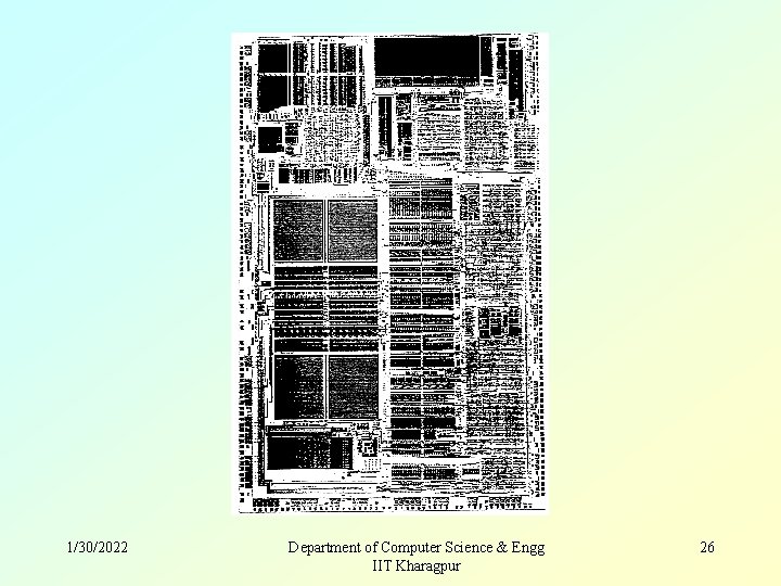
Contd. • In real full-custom layout in which the geometry, orientation and placement of every transistor is done individually by the designer, – Design productivity is usually very low. • Typically 10 to 20 transistors per day, per designer. • In digital CMOS VLSI, full-custom design is rarely used due to the high labor cost. – Exceptions to this include the design of high-volume products such as memory chips, high-performance microprocessors and FPGA masters. • Next slide shows the full layout of the Intel 486 P chip. – Good example of a hybrid full-custom design. 1/30/2022 Department of Computer Science & Engg IIT Kharagpur 25

1/30/2022 Department of Computer Science & Engg IIT Kharagpur 26

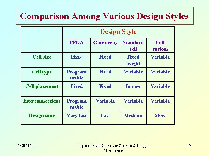
Comparison Among Various Design Style FPGA Gate array Standard cell Full custom Cell size Fixed height Variable Cell type Program mable Fixed Variable Cell placement Fixed In row Variable Interconnections Program mable Variable Design time Very fast Fast Medium Slow 1/30/2022 Department of Computer Science & Engg IIT Kharagpur 27

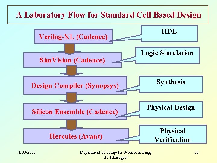
A Laboratory Flow for Standard Cell Based Design HDL Verilog-XL (Cadence) Sim. Vision (Cadence) Logic Simulation Synthesis Design Compiler (Synopsys) Silicon Ensemble (Cadence) Physical Design Hercules (Avant) 1/30/2022 Department of Computer Science & Engg IIT Kharagpur Physical Verification 28

Introduction To Verilog-HDL 1/30/2022 Department of Computer Science & Engg IIT Kharagpur 29

How it started! • • Gateway Design Automation Cadence purchased Gateway in 1989. Verilog was placed in the public domain. Open Verilog International (OVI) was created to develop the Verilog Language as IEEE standard. 1/30/2022 Department of Computer Science & Engg IIT Kharagpur 30

The Verilog Language • • • Originally a modeling language for a very efficient event-driven digital logic simulator Later pushed into use as a specification language for logic synthesis Now, one of the two most commonly-used languages in digital hardware design (VHDL is the other) Virtually every chip (FPGA, ASIC, etc. ) is designed in part using one of these two languages Combines structural and behavioral modeling styles 1/30/2022 Department of Computer Science & Engg IIT Kharagpur 31

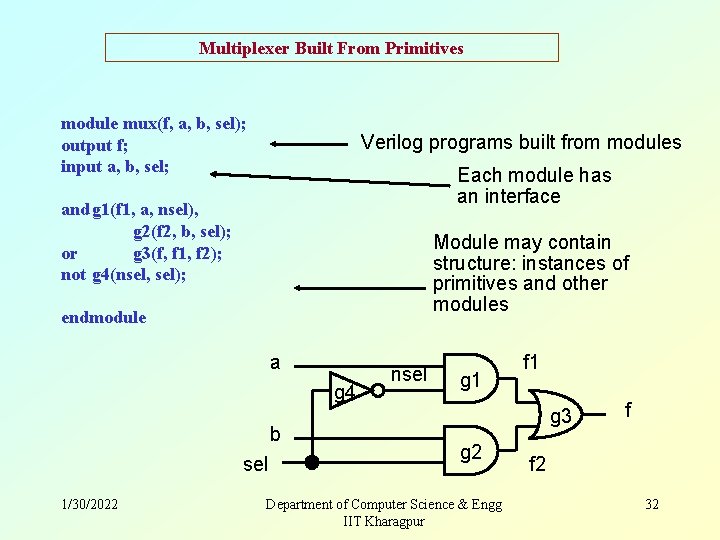
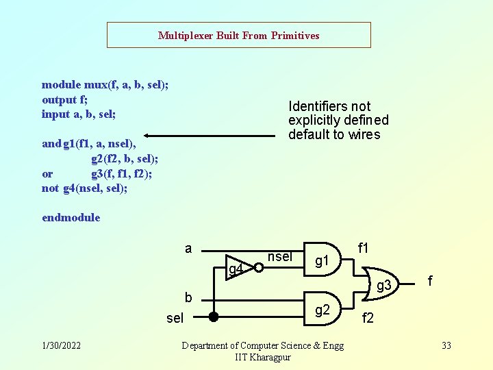
Multiplexer Built From Primitives module mux(f, a, b, sel); output f; input a, b, sel; Verilog programs built from modules Each module has an interface andg 1(f 1, a, nsel), g 2(f 2, b, sel); or g 3(f, f 1, f 2); not g 4(nsel, sel); Module may contain structure: instances of primitives and other modules endmodule a g 4 b sel 1/30/2022 nsel g 1 f 1 g 3 g 2 Department of Computer Science & Engg IIT Kharagpur f f 2 32

Multiplexer Built From Primitives module mux(f, a, b, sel); output f; input a, b, sel; Identifiers not explicitly defined default to wires andg 1(f 1, a, nsel), g 2(f 2, b, sel); or g 3(f, f 1, f 2); not g 4(nsel, sel); endmodule a g 4 b sel 1/30/2022 nsel g 1 f 1 g 3 g 2 Department of Computer Science & Engg IIT Kharagpur f f 2 33

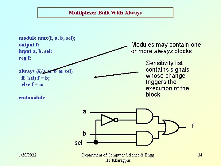
Multiplexer Built With Always module mux(f, a, b, sel); output f; input a, b, sel; reg f; Modules may contain one or more always blocks Sensitivity list contains signals whose change triggers the execution of the block always @(a or b or sel) if (sel) f = b; else f = a; endmodule a f b sel 1/30/2022 Department of Computer Science & Engg IIT Kharagpur 34

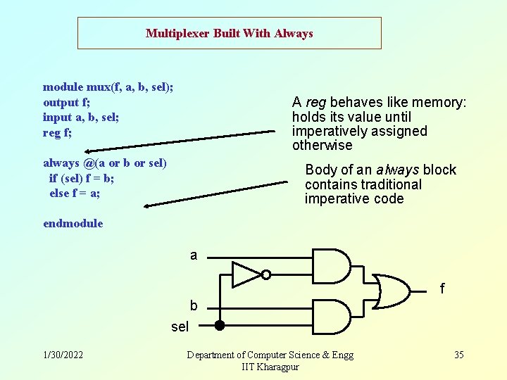
Multiplexer Built With Always module mux(f, a, b, sel); output f; input a, b, sel; reg f; A reg behaves like memory: holds its value until imperatively assigned otherwise always @(a or b or sel) if (sel) f = b; else f = a; Body of an always block contains traditional imperative code endmodule a f b sel 1/30/2022 Department of Computer Science & Engg IIT Kharagpur 35

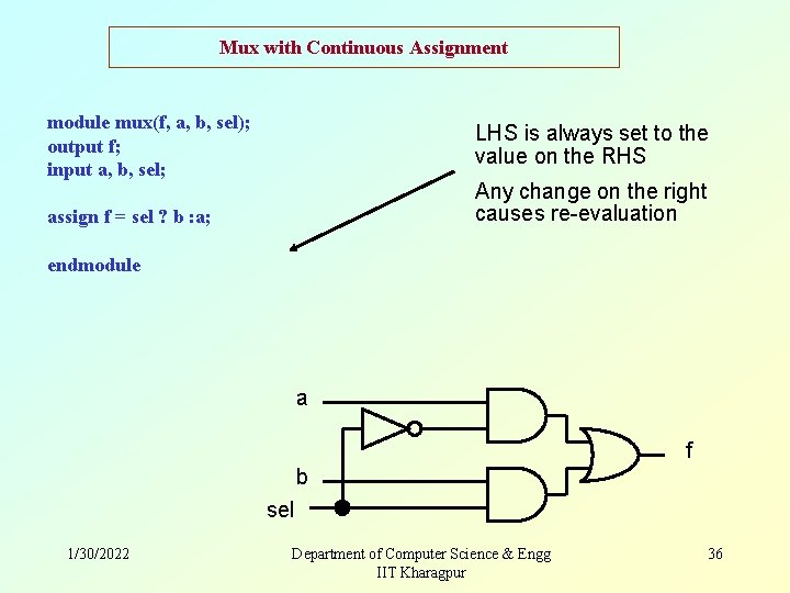
Mux with Continuous Assignment module mux(f, a, b, sel); output f; input a, b, sel; LHS is always set to the value on the RHS Any change on the right causes re-evaluation assign f = sel ? b : a; endmodule a f b sel 1/30/2022 Department of Computer Science & Engg IIT Kharagpur 36

Identifiers in Verilog • Any Sequence of letter, digits, dollar sign, underscore. • First character must be a letter or underscore. • It cannot be a dollar sign. • Cannot use characters such as hyphen, brackets, or # in verilog names 1/30/2022 Department of Computer Science & Engg IIT Kharagpur 37

Verilog Logic Values • Predefined logic value system or value set : ‘ 0’, ‘ 1’ , ’x’ and ‘z’; • ‘x’ means uninitialized or unknown logic value • ‘z’ means high impedance value. 1/30/2022 Department of Computer Science & Engg IIT Kharagpur 38

Verilog Data Types • Nets: wire, supply 1, supply 0 • Registers. • Wire: i) Analogous to a wire in an ASIC. ii) Cannot store or hold a value. • Integer 1/30/2022 Department of Computer Science & Engg IIT Kharagpur 39

The Register Data Type • Register Data Type: Comparable to a variable in a programming language. • Default initial value: ‘x’ • • • module reg_ex 1; reg Q; wire D; always @(posedge clk) Q=D; A reg is not always equivalent to a hardware register, flipflop or latch. module reg_ex 2; // purely combinational reg c; always @(a or b) c=a|b; endmodule 1/30/2022 Department of Computer Science & Engg IIT Kharagpur 40

Numbers • Format of integer constants: Width’ radix value; • Verilog keeps track of the sign if it is assigned to an integer or assigned to a parameter. • Once verilog looses sign the designer has to be careful. 1/30/2022 Department of Computer Science & Engg IIT Kharagpur 41

Hierarchy • Module interface provides the means to interconnect two verilog modules. • Note that a reg cannot be an input/ inout port. • A module may instantiate other modules. 1/30/2022 Department of Computer Science & Engg IIT Kharagpur 42

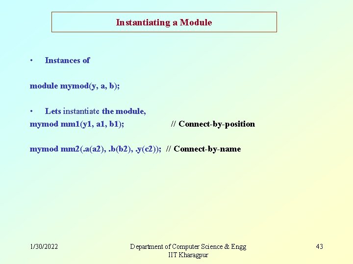
Instantiating a Module • Instances of module mymod(y, a, b); • Lets instantiate the module, mymod mm 1(y 1, a 1, b 1); // Connect-by-position mymod mm 2(. a(a 2), . b(b 2), . y(c 2)); // Connect-by-name 1/30/2022 Department of Computer Science & Engg IIT Kharagpur 43

Sequential Blocks • Sequential block is a group of statements between a begin and an end. • A sequential block, in an always statement executes repeatedly. • Inside an initial statement, it operates only once. 1/30/2022 Department of Computer Science & Engg IIT Kharagpur 44

Procedures • A Procedure is an always or initial statement or a function. • Procedural statements within a sequential block executes concurrently with other procedures. 1/30/2022 Department of Computer Science & Engg IIT Kharagpur 45

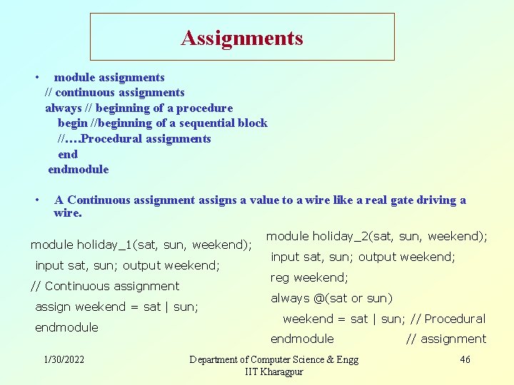
Assignments • • module assignments // continuous assignments always // beginning of a procedure begin //beginning of a sequential block //…. Procedural assignments endmodule A Continuous assignment assigns a value to a wire like a real gate driving a wire. module holiday_1(sat, sun, weekend); input sat, sun; output weekend; // Continuous assignment assign weekend = sat | sun; endmodule 1/30/2022 module holiday_2(sat, sun, weekend); input sat, sun; output weekend; reg weekend; always @(sat or sun) weekend = sat | sun; // Procedural endmodule Department of Computer Science & Engg IIT Kharagpur // assignment 46

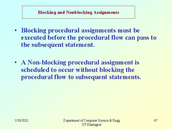
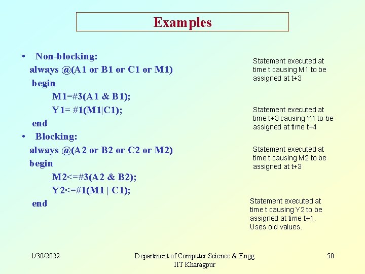
Blocking and Nonblocking Assignments • Blocking procedural assignments must be executed before the procedural flow can pass to the subsequent statement. • A Non-blocking procedural assignment is scheduled to occur without blocking the procedural flow to subsequent statements. 1/30/2022 Department of Computer Science & Engg IIT Kharagpur 47

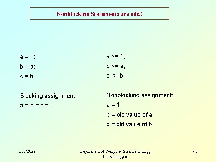
Nonblocking Statements are odd! a = 1; a <= 1; b = a; b <= a; c = b; c <= b; Blocking assignment: Nonblocking assignment: a=b=c=1 a=1 b = old value of a c = old value of b 1/30/2022 Department of Computer Science & Engg IIT Kharagpur 48

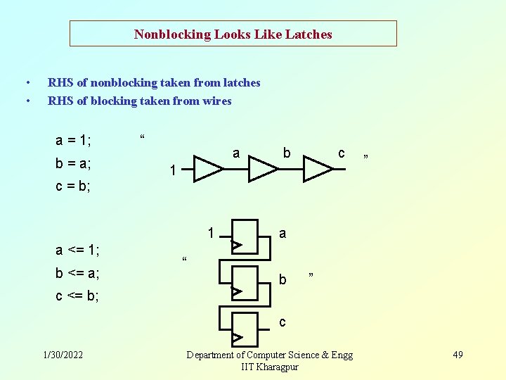
Nonblocking Looks Like Latches • • RHS of nonblocking taken from latches RHS of blocking taken from wires a = 1; b = a; “ a b c 1 ” c = b; 1 a <= 1; b <= a; a “ b ” c <= b; c 1/30/2022 Department of Computer Science & Engg IIT Kharagpur 49

Examples • Non-blocking: always @(A 1 or B 1 or C 1 or M 1) begin M 1=#3(A 1 & B 1); Y 1= #1(M 1|C 1); end • Blocking: always @(A 2 or B 2 or C 2 or M 2) begin M 2<=#3(A 2 & B 2); Y 2<=#1(M 1 | C 1); end 1/30/2022 Statement executed at time t causing M 1 to be assigned at t+3 Statement executed at time t+3 causing Y 1 to be assigned at time t+4 Statement executed at time t causing M 2 to be assigned at t+3 Statement executed at time t causing Y 2 to be assigned at time t+1. Uses old values. Department of Computer Science & Engg IIT Kharagpur 50
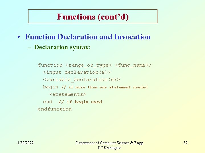
![Parameterized Design module vectorandz a b parameter cardinality 1 input cardinality1 0 Parameterized Design • module vector_and(z, a, b); parameter cardinality = 1; input [cardinality-1: 0]](https://slidetodoc.com/presentation_image_h2/97005fef38ac1b69353d041a59e0ef9b/image-51.jpg)
Parameterized Design • module vector_and(z, a, b); parameter cardinality = 1; input [cardinality-1: 0] a, b; output [cardinality-1: 0] z; wire [cardinality-1: 0] z = a & b; endmodule • We override these parameters when we instantiate the module as: module Four_and_gates(Out. Bus, In. Bus. A, In. Bus. B); input [3: 0] In. Bus. A, In. Bus. B; output[3: 0] Out. Bus; Vector_And #(4) My_And(Out. Bus, In. Bus. A, In. Bus. B); endmodule 1/30/2022 Department of Computer Science & Engg IIT Kharagpur 51

Functions (cont’d) • Function Declaration and Invocation – Declaration syntax: function <range_or_type> <func_name>; <input declaration(s)> <variable_declaration(s)> begin // if more than one statement needed <statements> end // if begin used endfunction 1/30/2022 Department of Computer Science & Engg IIT Kharagpur 52

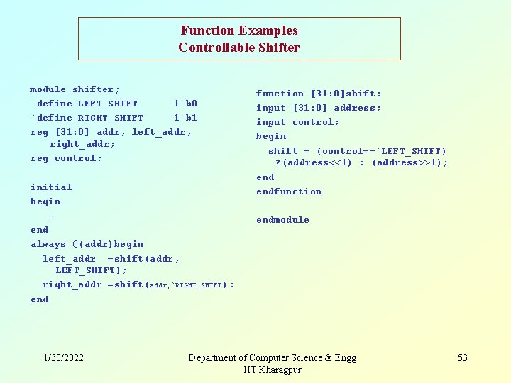
Function Examples Controllable Shifter module shifter; `define LEFT_SHIFT 1'b 0 `define RIGHT_SHIFT 1'b 1 reg [31: 0] addr, left_addr, right_addr; reg control; initial begin … end always @(addr)begin left_addr =shift(addr, `LEFT_SHIFT); right_addr =shift(addr, `RIGHT_SHIFT); end 1/30/2022 function [31: 0]shift; input [31: 0] address; input control; begin shift = (control==`LEFT_SHIFT) ? (address<<1) : (address>>1); endfunction endmodule Department of Computer Science & Engg IIT Kharagpur 53

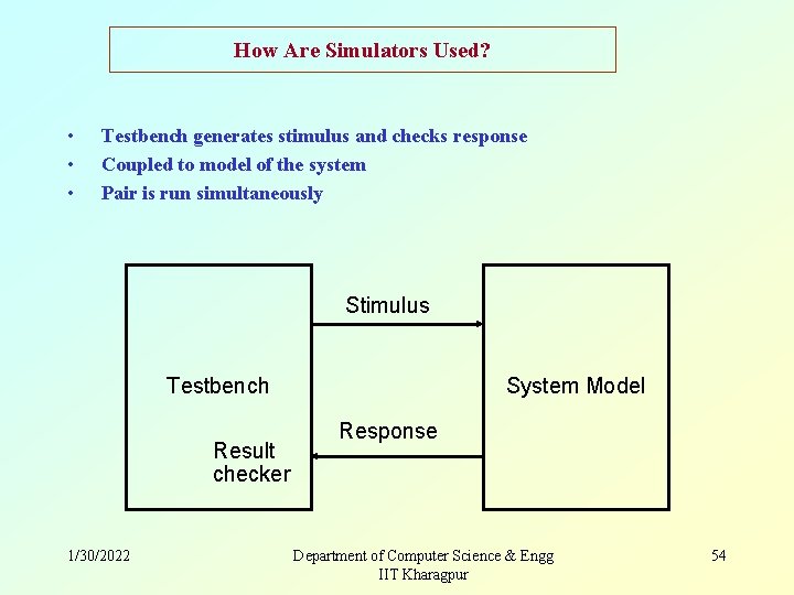
How Are Simulators Used? • • • Testbench generates stimulus and checks response Coupled to model of the system Pair is run simultaneously Stimulus Testbench Result checker 1/30/2022 System Model Response Department of Computer Science & Engg IIT Kharagpur 54

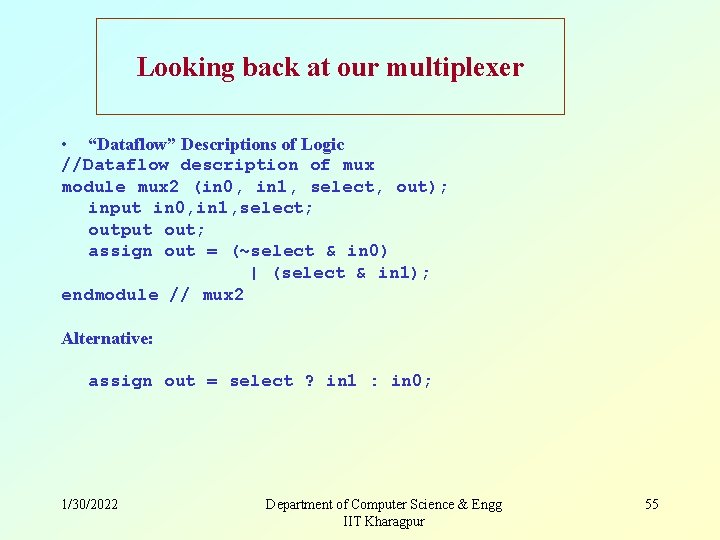
Looking back at our multiplexer • “Dataflow” Descriptions of Logic //Dataflow description of mux module mux 2 (in 0, in 1, select, out); input in 0, in 1, select; output out; assign out = (~select & in 0) | (select & in 1); endmodule // mux 2 Alternative: assign out = select ? in 1 : in 0; 1/30/2022 Department of Computer Science & Engg IIT Kharagpur 55

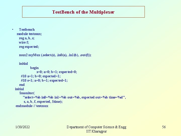
Test. Bench of the Multiplexer • Testbench module testmux; reg a, b, s; wire f; reg expected; mux 2 my. Mux (. select(s), . in 0(a), . in 1(b), . out(f)); initial begin s=0; a=0; b=1; expected=0; #10 a=1; b=0; expected=1; #10 s=1; a=0; b=1; expected=1; end initial $monitor( "select=%b in 0=%b in 1=%b out=%b, expected out=%b time=%d", s, a, b, f, expected, $time); endmodule // testmux 1/30/2022 Department of Computer Science & Engg IIT Kharagpur 56

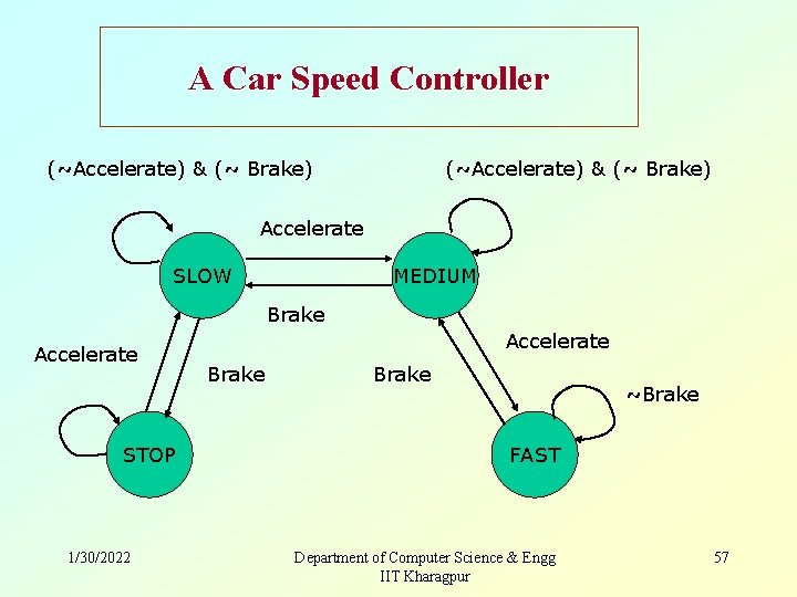
A Car Speed Controller (~Accelerate) & (~ Brake) Accelerate SLOW MEDIUM Brake Accelerate STOP 1/30/2022 Accelerate Brake ~Brake FAST Department of Computer Science & Engg IIT Kharagpur 57

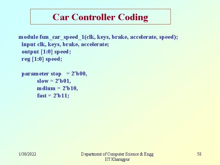
Car Controller Coding module fsm_car_speed_1(clk, keys, brake, accelerate, speed); input clk, keys, brake, accelerate; output [1: 0] speed; reg [1: 0] speed; parameter stop = 2'b 00, slow = 2'b 01, mdium = 2'b 10, fast = 2'b 11; 1/30/2022 Department of Computer Science & Engg IIT Kharagpur 58

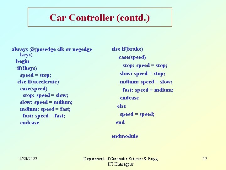
Car Controller (contd. ) always @(posedge clk or negedge keys) begin if(!keys) speed = stop; else if(accelerate) case(speed) stop: speed = slow; slow: speed = mdium; mdium: speed = fast; fast: speed = fast; endcase else if(brake) case(speed) stop: speed = stop; slow: speed = stop; mdium: speed = slow; fast: speed = mdium; endcase else speed = speed; endmodule 1/30/2022 Department of Computer Science & Engg IIT Kharagpur 59

A Better Way! • We keep a separate control part where the next state is calculated. • The other part generates the output from the next state. • We follow this architecture in the coding of any finite state machines, like ALU, etc. ( to be discussed later) 1/30/2022 Department of Computer Science & Engg IIT Kharagpur 60
![module fsmcarspeed2clk keys brake accelerate speed input clk keys brake accelerate output 1 0 module fsm_car_speed_2(clk, keys, brake, accelerate, speed); input clk, keys, brake, accelerate; output [1: 0]](https://slidetodoc.com/presentation_image_h2/97005fef38ac1b69353d041a59e0ef9b/image-61.jpg)
module fsm_car_speed_2(clk, keys, brake, accelerate, speed); input clk, keys, brake, accelerate; output [1: 0] speed; reg [1: 0] newspeed; parameter stop = 2'b 00, slow = 2'b 01, mdium = 2'b 10, fast = 2'b 11; always @(keys or brake or accelerate or speed) begin case(speed) stop: if(accelerate) newspeed = slow; else newspeed = stop; 1/30/2022 slow: if(brake) newspeed = stop; else if(accelerate) newspeed = mdium; else newspeed = slow; mdium: if(brake) newspeed = slow; else if(accelerate) newspeed = fast; else newspeed = mdium; fast: if(brake) newspeed = mdium; else newspeed = fast; default: newspeed = stop; endcase end Department of Computer Science & Engg IIT Kharagpur always @(posedge clk or negedge keys) begin if(!keys) speed = stop; else speed = newspeed; endmodule 61

Conclusion : Write codes which can be translated into hardware ! The following cannot be translated into hardware( non - synthesizable): • Initial blocks – Used to set up initial state or describe finite testbench stimuli – Don’t have obvious hardware component • Delays – May be in the Verilog source, but are simply ignored • In short, write codes with a hardware in your mind. In other words do not depend too much upon the tool to decide upon the resultant hardware. • Finally, remember that you are a better designer than the tool. 1/30/2022 Department of Computer Science & Engg IIT Kharagpur 62