Digital Fundamentals Tenth Edition Floyd Combinational Logic Analysis

Digital Fundamentals Tenth Edition Floyd Combinational Logic Analysis Floyd, Digital Fundamentals, 10 th ed sunwq@sjtu. edu. cn © 2008 Pearson Education Shanghai Jiao Tong University

In this chapter • Objectives – Analysis of combinational logic – Implementation of combinational logic – NAND/NOR universal gates and applications – OC gates/Tri-state gates • Reading assignment – Read chapter 5 in the text Floyd, Digital Fundamentals, 10 th ed sunwq@sjtu. edu. cn Shanghai Jiao Tong University
 form, basic combinational circuits can be directly implemented")
Combinational Logic Circuits In Sum-of-Products (SOP) form, basic combinational circuits can be directly implemented with AND-OR combinations if the necessary complement terms are available. Floyd, Digital Fundamentals, 10 th ed sunwq@sjtu. edu. cn Shanghai Jiao Tong University

Combinational Logic Circuits An example of an SOP implementation is shown. The SOP expression is an AND-OR combination of the input variables and the appropriate complements. A B C ABC X = ABC + DE SOP D E Floyd, Digital Fundamentals, 10 th ed DE sunwq@sjtu. edu. cn Shanghai Jiao Tong University

Combinational Logic Circuits When the output of a SOP form is inverted, the circuit is called an AND-OR-Invert circuit. The AOI configuration lends itself to product-of-sums (POS) implementation. An example of an AOI implementation is shown. The output expression can be changed to a POS expression by applying De. Morgan’s theorem twice. A B C ABC X = ABC + DE Floyd, Digital Fundamentals, 10 th ed AOI X = (ABC)(DE) De. Morgan D E X = ABC + DE DE X = (A + B + C)(D + E) POS sunwq@sjtu. edu. cn Shanghai Jiao Tong University

Exclusive-OR Logic The truth table for an exclusive-OR gate is Notice that the output is HIGH whenever A and B disagree. The Boolean expression is X = AB + AB The circuit can be drawn as A Symbols: X Distinctive shape Rectangular outline B Floyd, Digital Fundamentals, 10 th ed sunwq@sjtu. edu. cn Shanghai Jiao Tong University

Exclusive-NOR Logic The truth table for an exclusive-NOR gate is Notice that the output is HIGH whenever A and B agree. The Boolean expression is X = AB + AB The circuit can be drawn as A X Symbols: B Distinctive shape Floyd, Digital Fundamentals, 10 th ed sunwq@sjtu. edu. cn Rectangular outline Shanghai Jiao Tong University
 (b)")
For each circuit, determine if the LED should be on or off. (a) (b) (c) Circuit (a): XOR, inputs agree, output is LOW, LED is ON. Circuit (b): XNOR, inputs disagree, output is LOW, LED is ON. Circuit (c): XOR, inputs disagree, output is HIGH, LED is OFF. Floyd, Digital Fundamentals, 10 th ed sunwq@sjtu. edu. cn Shanghai Jiao Tong University

Implementing Combinational Logic Implementing a SOP expression is done by first forming the AND terms; then the terms are ORed together. Show the circuit that will implement the Boolean expression X = ABC + ABD + BDE. (Assume that the variables and their complements are available. ) Start by forming the terms using three 3 -input AND gates. Then combine three terms using a 3 -input OR gate. A B C A B D X = ABC + ABD + BDE B D E Floyd, Digital Fundamentals, 10 th ed sunwq@sjtu. edu. cn Shanghai Jiao Tong University

Karnaugh Map Implementation For basic combinational logic circuits, the Karnaugh map can be read and the circuit drawn as a minimum SOP. A Karnaugh map is drawn from a truth table. Read the minimum SOP expression and draw the circuit. 1. Group the 1’s into two overlapping groups as indicated. 2. Read each group by eliminating any variable that changes across a boundary. B changes across this boundary 3. The vertical group is read A C. C changes across this boundary Floyd, Digital Fundamentals, 10 th ed 4. The horizontal group is read AB. The circuit is on the next slide: sunwq@sjtu. edu. cn Shanghai Jiao Tong University

continued… Circuit: A C X= AC + AB A B The result is shown as a sum of products. It is a simple matter to implement this form using only NAND gates as shown in the text and following example. Floyd, Digital Fundamentals, 10 th ed sunwq@sjtu. edu. cn Shanghai Jiao Tong University

NAND Logic Convert the circuit in the previous example to one that uses only NAND gates. Recall from Boolean algebra that double inversion cancels. By adding inverting bubbles to above circuit, it is easily converted to NAND gates: A C X= AC + AB A B Floyd, Digital Fundamentals, 10 th ed sunwq@sjtu. edu. cn Shanghai Jiao Tong University

Universal Gates NAND gates are sometimes called universal gates because they can be used to produce the other basic Boolean functions. A A B A Inverter AB AND gate A A A+B B B OR gate Floyd, Digital Fundamentals, 10 th ed NOR gate sunwq@sjtu. edu. cn Shanghai Jiao Tong University

Universal Gates NOR gates are also universal gates and can form all of the basic gates. A A B A Inverter A+ B OR gate A A AB AB B B AND gate Floyd, Digital Fundamentals, 10 th ed NAND gate sunwq@sjtu. edu. cn Shanghai Jiao Tong University

NAND Logic Recall from De. Morgan’s theorem that AB = A + B. By using equivalent symbols, it is simpler to read the logic of SOP forms. The earlier example shows the idea: A C X= AC + AB A B The logic is easy to read if you (mentally) cancel the two connected bubbles on a line. Floyd, Digital Fundamentals, 10 th ed sunwq@sjtu. edu. cn Shanghai Jiao Tong University

NOR Logic Alternatively, De. Morgan’s theorem can be written as A + B = A B. By using equivalent symbols, it is simpler to read the logic of POS forms. For example, A B X = (A + B)(A + C) A C Again, the logic is easy to read if you cancel the two connected bubbles on a line. Floyd, Digital Fundamentals, 10 th ed sunwq@sjtu. edu. cn Shanghai Jiao Tong University

Pulsed Waveforms For combinational circuits with pulsed inputs, the output can be predicted by developing intermediate outputs and combining the result. For example, the circuit shown can be analyzed at the outputs of the OR gates: A B C D G 1 G 3 G 2 G 1 G 2 G 3 Floyd, Digital Fundamentals, 10 th ed sunwq@sjtu. edu. cn Shanghai Jiao Tong University

Pulsed Waveforms Alternatively, you can develop the truth table for the circuit and enter 0’s and 1’s on the waveforms. Then read the output from the table. A B G 1 G 3 C G 2 D A 0 1 0 1 0 1 B 0 1 1 0 0 0 C 0 0 0 1 1 0 0 0 D G 3 0 0 0 0 1 1 1 0 Floyd, Digital Fundamentals, 10 th ed sunwq@sjtu. edu. cn Inputs Output A B C D X 0 0 0 0 1 1 1 1 0 0 0 1 1 1 0 0 0 0 1 1 1 1 0 0 1 1 0 1 0 1 Shanghai Jiao Tong University
 • Wired-AND(线与) • Tri-state gate(三态门) Floyd, Digital Fundamentals,")
Other gates • Open Collector gate(集电极开路门电路) • Wired-AND(线与) • Tri-state gate(三态门) Floyd, Digital Fundamentals, 10 th ed sunwq@sjtu. edu. cn Shanghai Jiao Tong University

A standard TTL inverter circuit Floyd, Digital Fundamentals, 10 th ed sunwq@sjtu. edu. cn Shanghai Jiao Tong University

Operation of a TTL inverter Floyd, Digital Fundamentals, 10 th ed sunwq@sjtu. edu. cn Shanghai Jiao Tong University

Open collector gate Floyd, Digital Fundamentals, 10 th ed sunwq@sjtu. edu. cn Shanghai Jiao Tong University

A wired-AND configuration of four inverters Floyd, Digital Fundamentals, 10 th ed sunwq@sjtu. edu. cn Shanghai Jiao Tong University

Open-collector wired negative-AND operation with inverters Floyd, Digital Fundamentals, 10 th ed sunwq@sjtu. edu. cn Shanghai Jiao Tong University

Wired-AND Determine X as a function of A~F X = ABCDEF Floyd, Digital Fundamentals, 10 th ed sunwq@sjtu. edu. cn Shanghai Jiao Tong University

Driving and loading concepts Floyd, Digital Fundamentals, 10 th ed sunwq@sjtu. edu. cn Shanghai Jiao Tong University
 Floyd, Digital Fundamentals, 10 th ed sunwq@sjtu. edu.")
Driving and loading concepts (in TTL) Floyd, Digital Fundamentals, 10 th ed sunwq@sjtu. edu. cn Shanghai Jiao Tong University

Handling unused CMOS inputs Floyd, Digital Fundamentals, 10 th ed sunwq@sjtu. edu. cn Shanghai Jiao Tong University

Tri-state Gates Truth Table A B 1 0 0 X 1 0 F Z 0 1 high impedance state normal states • Tri-state : – if the switch is closed: two valid logic states (high or low) – If the switch is open: high impedance state Floyd, Digital Fundamentals, 10 th ed sunwq@sjtu. edu. cn Shanghai Jiao Tong University

Tri-state Gates Floyd, Digital Fundamentals, 10 th ed sunwq@sjtu. edu. cn Shanghai Jiao Tong University

Example: Bus structure with tri-state gates Bus is 1 1 1 IOH 0 IOZ 1 0 IIH 0 0 Bus is 0 IOL 0 0 IOZ 1 0 BUS 1 Floyd, Digital Fundamentals, 10 th ed IOZ 1 BUS IIL IOZ 0 sunwq@sjtu. edu. cn IIH 0 IIL IIZ 1 Shanghai Jiao Tong University

Application Example: Transceiver Floyd, Digital Fundamentals, 10 th ed sunwq@sjtu. edu. cn Shanghai Jiao Tong University

Selected Key Terms Universal gate Either a NAND or a NOR gate. The term universal refers to a property of a gate that permits any logic function to be implemented by that gate or by a combination of gates of that kind. Negative-OR The dual operation of a NAND gate when the inputs are active-LOW. Negative-AND The dual operation of a NOR gate when the inputs are active-LOW. Floyd, Digital Fundamentals, 10 th ed sunwq@sjtu. edu. cn Shanghai Jiao Tong University
, 4(d, e), 8, 10(g), 16, 20, 22, 26(g),")
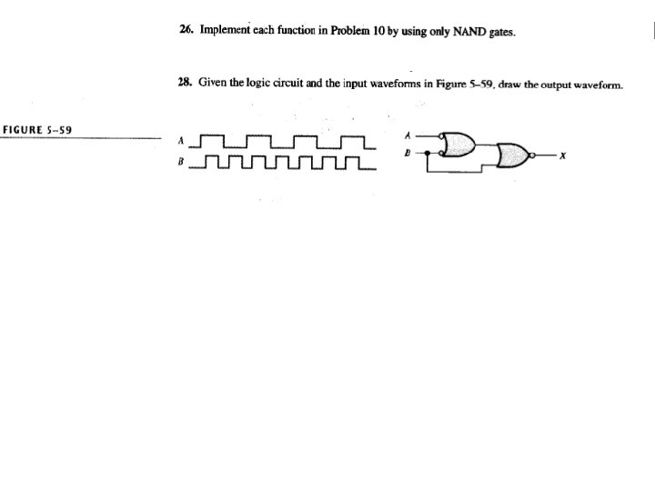
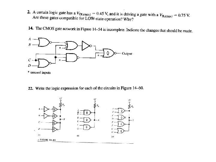
Homework • pp. 274 • 2(b), 4(d, e), 8, 10(g), 16, 20, 22, 26(g), 28 • pp. 801 • 2, 14, 22 Floyd, Digital Fundamentals, 10 th ed sunwq@sjtu. edu. cn Shanghai Jiao Tong University

1. Assume an AOI expression is AB + CD. The equivalent POS expression is a. (A + B)(C + D) b. (A + B)(C + D) c. (A + B)(C + D) d. none of the above Floyd, Digital Fundamentals, 10 th ed sunwq@sjtu. edu. cn Shanghai Jiao Tong University © 2008 Pearson Education

2. The truth table shown is for a. a NAND gate b. a NOR gate c. an exclusive-OR gate d. an exclusive-NOR gate Floyd, Digital Fundamentals, 10 th ed sunwq@sjtu. edu. cn Shanghai Jiao Tong University © 2008 Pearson Education

3. An LED that should be ON is a. LED-1 b. LED-2 c. neither d. both Floyd, Digital Fundamentals, 10 th ed sunwq@sjtu. edu. cn Shanghai Jiao Tong University © 2008 Pearson Education

4. To implement the SOP expression X = ABC + ABD + BDE , the type of gate that is needed is a a. 3 -input AND gate b. 3 -input NAND gate c. 3 -input OR gate d. 3 -input NOR gate Floyd, Digital Fundamentals, 10 th ed sunwq@sjtu. edu. cn A B C A B D E Shanghai Jiao Tong University © 2008 Pearson Education

5. Reading the Karnaugh map, the logic expression is a. A C + A B b. A B + A C c. A B + B C d. A B + A C Floyd, Digital Fundamentals, 10 th ed sunwq@sjtu. edu. cn Shanghai Jiao Tong University © 2008 Pearson Education

6. The circuit shown will have identical logic out if all gates are changed to a. AND gates A B b. OR gates c. NAND gates C D d. NOR gates Floyd, Digital Fundamentals, 10 th ed sunwq@sjtu. edu. cn Shanghai Jiao Tong University © 2008 Pearson Education

7. The two types of gates which are called universal gates are a. AND/OR b. NAND/NOR c. AND/NAND d. OR/NOR Floyd, Digital Fundamentals, 10 th ed sunwq@sjtu. edu. cn Shanghai Jiao Tong University © 2008 Pearson Education

8. The circuit shown is equivalent to an a. AND gate A b. XOR gate B c. OR gate d. none of the above Floyd, Digital Fundamentals, 10 th ed sunwq@sjtu. edu. cn Shanghai Jiao Tong University © 2008 Pearson Education

9. The circuit shown is equivalent to a. an AND gate b. an XOR gate A B c. an OR gate d. none of the above Floyd, Digital Fundamentals, 10 th ed sunwq@sjtu. edu. cn Shanghai Jiao Tong University © 2008 Pearson Education

10. During the first three intervals for the pulsed circuit shown, the output of a. G 1 is LOW and G 2 is LOW b. G 1 is LOW and G 2 is HIGH c. G 1 is HIGH and G 2 is LOW d. G 1 is HIGH and G 2 is HIGH A A B B C C D Floyd, Digital Fundamentals, 10 th ed D sunwq@sjtu. edu. cn G 1 G 3 G 2 Shanghai Jiao Tong University © 2008 Pearson Education

Answers: Floyd, Digital Fundamentals, 10 th ed 1. b 6. c 2. d 7. b 3. a 8. c 4. c 9. a 5. d 10. c sunwq@sjtu. edu. cn Shanghai Jiao Tong University
- Slides: 51