Digital Fundamentals DF GTU 3130704 Unit3 Sequential Circuits




- Slides: 45

Digital Fundamentals (DF) GTU # 3130704 Unit-3 Sequential Circuits and Systems Computer Engineering Department Darshan Institute of Engineering & Technology, Rajkot krunal. vyas@darshan. ac. in 9601901005

Looping Outline • Flip-flops o SR-FF, D-FF, JK-FF, T-FF • Registers o Buffer, Shift, Bidirectional, Universal • Asynchronous Counters o Ripple up-down, Modulo • Synchronous Counters o Up counter, Down counter using different FFs • Sequential Counters o Direct logic, Indirect logic

Section - 1

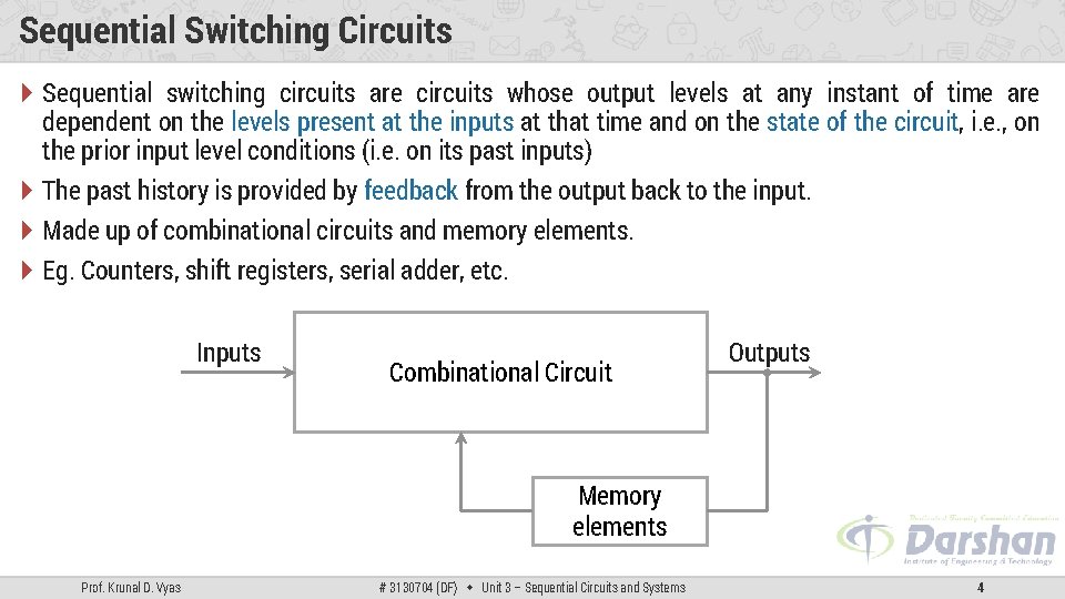
Sequential Switching Circuits Sequential switching circuits are circuits whose output levels at any instant of time are dependent on the levels present at the inputs at that time and on the state of the circuit, i. e. , on the prior input level conditions (i. e. on its past inputs) The past history is provided by feedback from the output back to the input. Made up of combinational circuits and memory elements. Eg. Counters, shift registers, serial adder, etc. Inputs Combinational Circuit Outputs Memory elements Prof. Krunal D. Vyas # 3130704 (DF) Unit 3 – Sequential Circuits and Systems 4

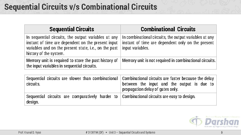
Sequential Circuits v/s Combinational Circuits Sequential Circuits Combinational Circuits In sequential circuits, the output variables at any instant of time are dependent on the present input variables and on the present state, i. e. , on the past history of the system. In combinational circuits, the output variables at any instant of time are dependent only on the present input variables. Memory unit is required to store the past history of the input variables in sequential circuits. Memory unit is not required in combinational circuits. Sequential circuits are slower than combinational circuits. Combinational circuits are faster because the delay between the input and the output is due to propagation delay of gates only. Sequential circuits are comparatively harder to design. Combinational circuits are easy to design. Prof. Krunal D. Vyas # 3130704 (DF) Unit 3 – Sequential Circuits and Systems 5

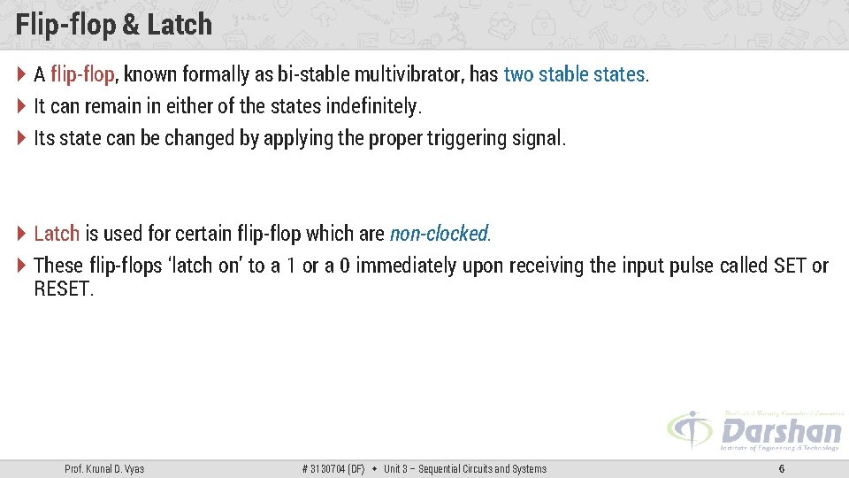
Flip-flop & Latch A flip-flop, known formally as bi-stable multivibrator, has two stable states. It can remain in either of the states indefinitely. Its state can be changed by applying the proper triggering signal. Latch is used for certain flip-flop which are non-clocked. These flip-flops ‘latch on’ to a 1 or a 0 immediately upon receiving the input pulse called SET or RESET. Prof. Krunal D. Vyas # 3130704 (DF) Unit 3 – Sequential Circuits and Systems 6

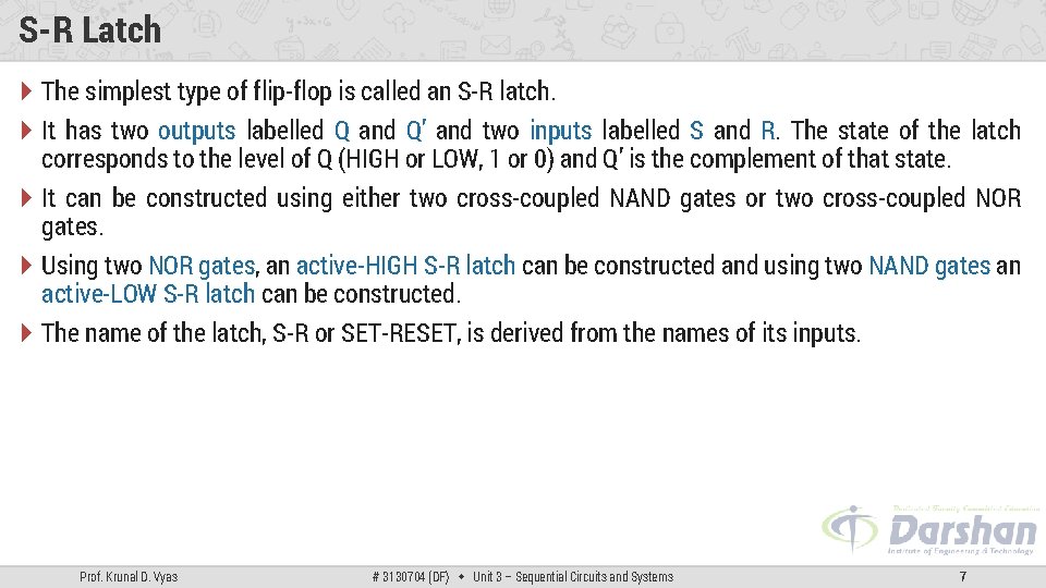
S-R Latch The simplest type of flip-flop is called an S-R latch. It has two outputs labelled Q and Q’ and two inputs labelled S and R. The state of the latch corresponds to the level of Q (HIGH or LOW, 1 or 0) and Q’ is the complement of that state. It can be constructed using either two cross-coupled NAND gates or two cross-coupled NOR gates. Using two NOR gates, an active-HIGH S-R latch can be constructed and using two NAND gates an active-LOW S-R latch can be constructed. The name of the latch, S-R or SET-RESET, is derived from the names of its inputs. Prof. Krunal D. Vyas # 3130704 (DF) Unit 3 – Sequential Circuits and Systems 7

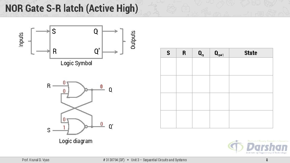
S Q R Q’ Outputs Inputs NOR Gate S-R latch (Active High) Logic Symbol R 0 0 0 S 1 01 0 Q Q’ S R Qn Qn+1 State 0 0 0 1 No Change 0 0 1 1 0 0 Reset 1 1 0 0 0 1 1 1 Set 1 1 0 1 x x Indeterminate (invalid) Logic diagram Prof. Krunal D. Vyas # 3130704 (DF) Unit 3 – Sequential Circuits and Systems 8

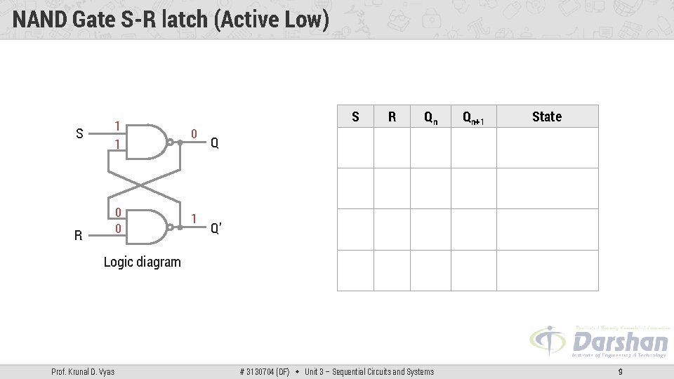
NAND Gate S-R latch (Active Low) 1 1 S 0 0 R Logic diagram Prof. Krunal D. Vyas 0 1 Q Q’ S R Qn Qn+1 State 0 0 0 1 x x Indeterminate (invalid) 0 0 1 1 1 Set 1 1 0 0 0 1 0 0 Reset 1 1 0 1 No Change # 3130704 (DF) Unit 3 – Sequential Circuits and Systems 9

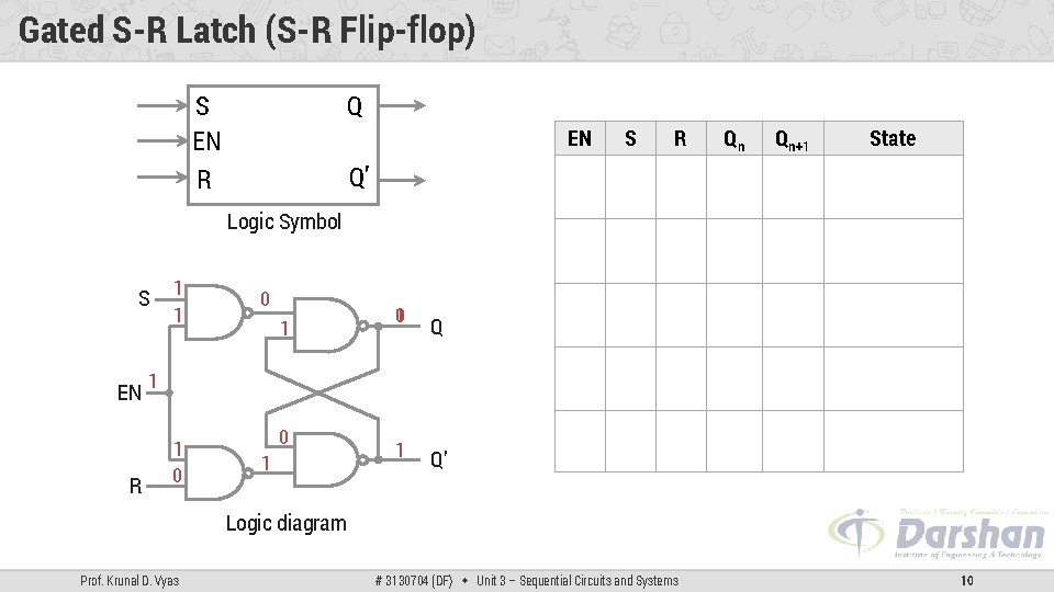
Gated S-R Latch (S-R Flip-flop) S EN R Q Q’ Logic Symbol S EN R 1 1 0 1 10 Q 1 1 0 0 1 1 Q’ EN S R Qn Qn+1 State 1 1 0 0 0 1 No Change 1 1 0 0 Reset 1 1 0 0 0 1 1 1 Set 1 1 1 0 1 x x 0 0 x x 0 1 Indeterminate (invalid) No Change Logic diagram Prof. Krunal D. Vyas # 3130704 (DF) Unit 3 – Sequential Circuits and Systems 10

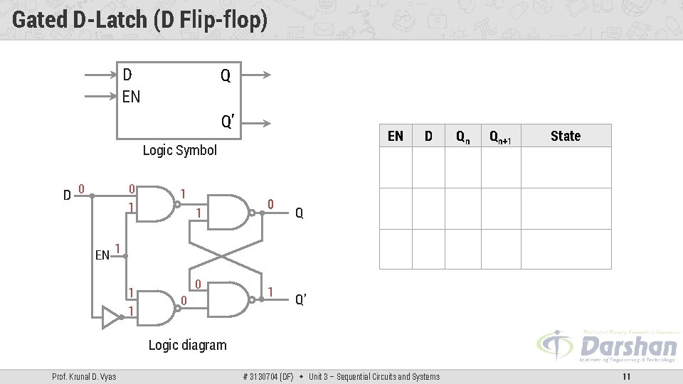
Gated D-Latch (D Flip-flop) D EN Q Q’ Logic Symbol 0 1 D 0 1 1 0 Q EN 1 1 1 0 0 1 EN D Qn Qn+1 State 1 1 0 0 0 1 0 0 Reset 1 1 0 1 1 1 Set 0 0 x x 0 1 No Change Q’ Logic diagram Prof. Krunal D. Vyas # 3130704 (DF) Unit 3 – Sequential Circuits and Systems 11

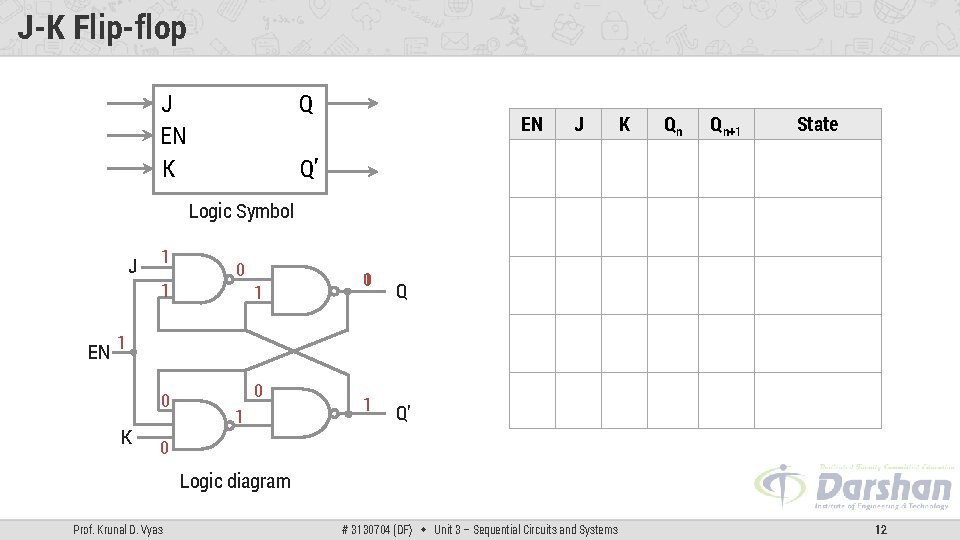
J-K Flip-flop J EN K Q Q’ Logic Symbol J 1 1 EN 0 1 01 Q 1 0 K 0 1 1 Q’ EN J K Qn Qn+1 State 1 1 0 0 0 1 No Change 1 1 0 0 Reset 1 1 0 0 0 1 1 1 Set 1 1 1 0 Toggle 0 0 x x 0 1 No Change 0 Logic diagram Prof. Krunal D. Vyas # 3130704 (DF) Unit 3 – Sequential Circuits and Systems 12

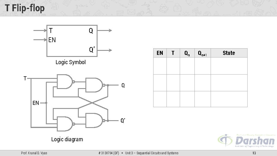
T Flip-flop T EN Q Q’ Logic Symbol T Q EN EN T Qn Qn+1 State 1 1 0 0 0 1 No change 1 1 0 Toggle 0 0 x x 0 1 No Change Q’ Logic diagram Prof. Krunal D. Vyas # 3130704 (DF) Unit 3 – Sequential Circuits and Systems 13

Section - 2

Registers As a flip-flop (FF) can store only one bit of data, a 0 or a 1, it is referred to as a single-bit register. A register is a set of FFs used to store binary data. The storage capacity of a register is the number of bits (1 s and 0 s) of digital data it can retain. Loading a register means setting or resetting the individual FFs, i. e. inputting data into the register so that their states correspond to the bits of data to be stored. Loading may be serial or parallel. In serial loading, data is transferred into the register in serial form i. e. one bit at a time. In parallel loading, the data is transferred into the register in parallel form meaning that all the FFs are triggered into their new states at the same time. Types of registers are: Buffer register, Shift register, Bidirectional shift register, Universal shift register Prof. Krunal D. Vyas # 3130704 (DF) Unit 3 – Sequential Circuits and Systems 15

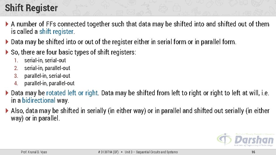
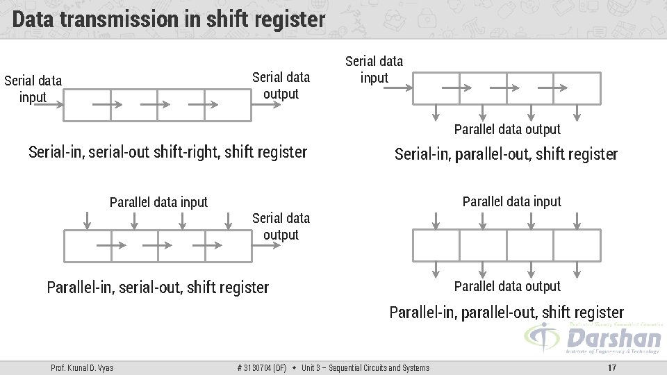
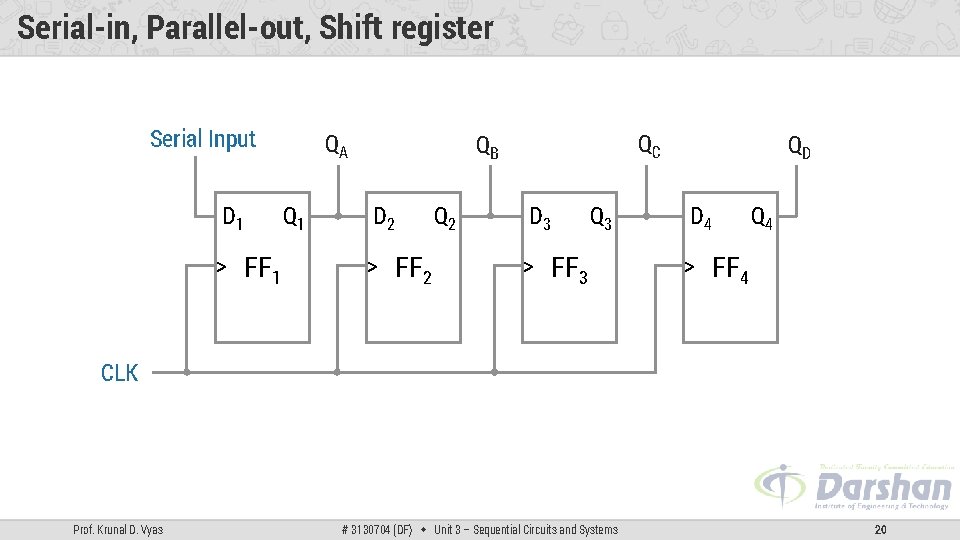
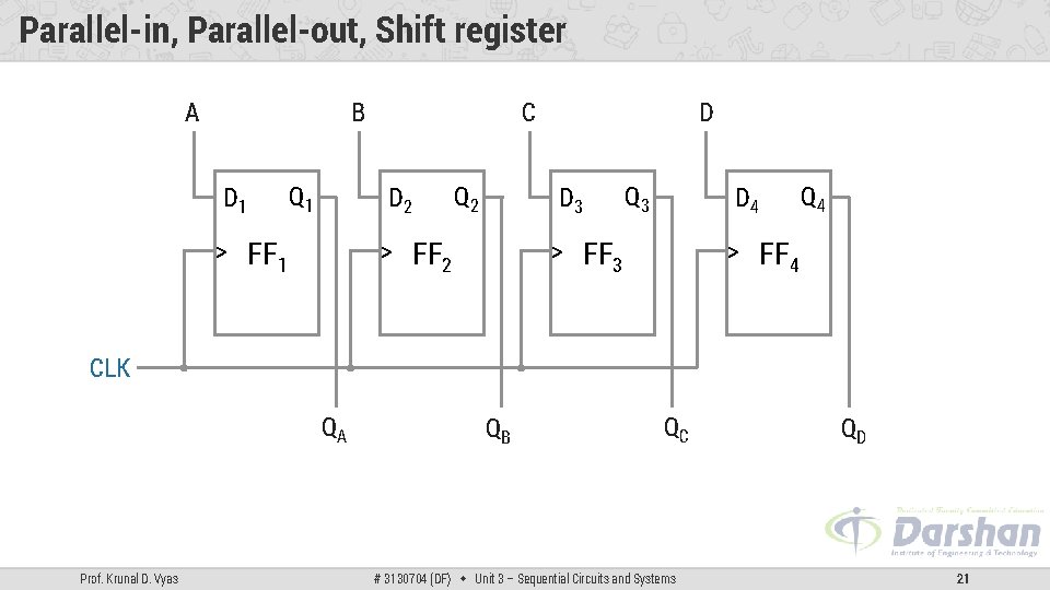
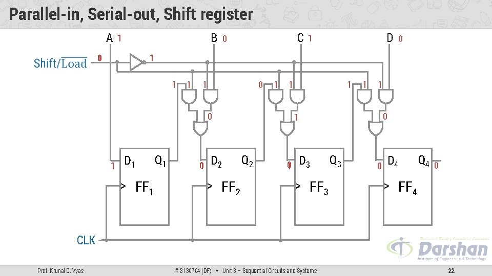
Shift Register A number of FFs connected together such that data may be shifted into and shifted out of them is called a shift register. Data may be shifted into or out of the register either in serial form or in parallel form. So, there are four basic types of shift registers: 1. 2. 3. 4. serial-in, serial-out serial-in, parallel-out parallel-in, serial-out parallel-in, parallel-out Data may be rotated left or right. Data may be shifted from left to right or right to left at will, i. e. in a bidirectional way. Also, data may be shifted in serially (in either way) or in parallel and shifted out serially (in either way) or in parallel. Prof. Krunal D. Vyas # 3130704 (DF) Unit 3 – Sequential Circuits and Systems 16

Data transmission in shift register Serial data output Serial data input Parallel data output Serial-in, serial-out shift-right, shift register Parallel data input Serial-in, parallel-out, shift register Parallel data input Serial data output Parallel-in, serial-out, shift register Parallel data output Parallel-in, parallel-out, shift register Prof. Krunal D. Vyas # 3130704 (DF) Unit 3 – Sequential Circuits and Systems 17

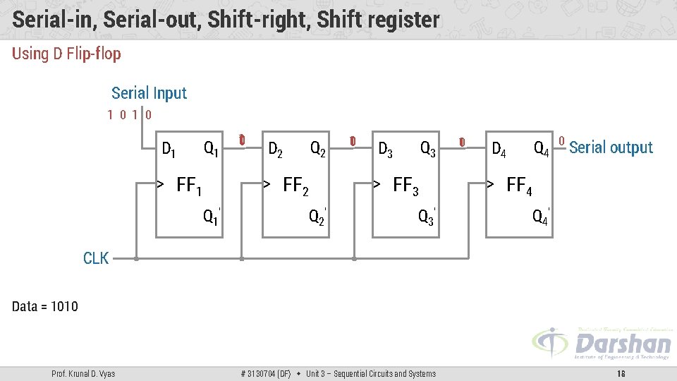
Serial-in, Serial-out, Shift-right, Shift register Using D Flip-flop Serial Input 1 0 D 1 Q 1 > FF 1 10 D 2 Q 2 > FF 2 Q 1’ 10 Q 3 D 3 > FF 3 Q 2’ Q 3’ 10 Q 4 D 4 0 Serial output > FF 4 Q 4’ CLK Data = 1010 Prof. Krunal D. Vyas # 3130704 (DF) Unit 3 – Sequential Circuits and Systems 18

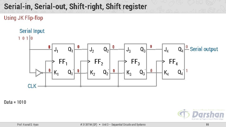
Serial-in, Serial-out, Shift-right, Shift register Using JK Flip-flop Serial Input 1 0 10 J 1 Q 1 01 > FF 1 01 K 1 J 2 Q 2 01 > FF 2 Q 1’ 01 K 2 Q 3 J 3 01 > FF 3 Q 2’ 01 K 3 Q 3’ Q 4 0 Q 4’ 1 J 4 Serial output > FF 4 01 K 4 CLK Data = 1010 Prof. Krunal D. Vyas # 3130704 (DF) Unit 3 – Sequential Circuits and Systems 19

Serial-in, Parallel-out, Shift register Serial Input D 1 > FF 1 QA Q 1 QC QB D 2 > FF 2 Q 2 D 3 Q 3 > FF 3 QD D 4 Q 4 > FF 4 CLK Prof. Krunal D. Vyas # 3130704 (DF) Unit 3 – Sequential Circuits and Systems 20

Parallel-in, Parallel-out, Shift register A C B D 1 Q 1 D 2 > FF 1 Q 2 D D 3 > FF 2 Q 3 D 4 > FF 3 Q 4 > FF 4 CLK QA Prof. Krunal D. Vyas QB QC # 3130704 (DF) Unit 3 – Sequential Circuits and Systems QD 21

Parallel-in, Serial-out, Shift register A B 1 01 C 0 D 1 0 1 1 1 0 1 D 1 > FF 1 Q 1 01 D 2 > FF 2 1 1 1 0 1 Q 2 01 D 3 > FF 3 Q 3 01 D 4 Q 4 0 > FF 4 CLK Prof. Krunal D. Vyas # 3130704 (DF) Unit 3 – Sequential Circuits and Systems 22

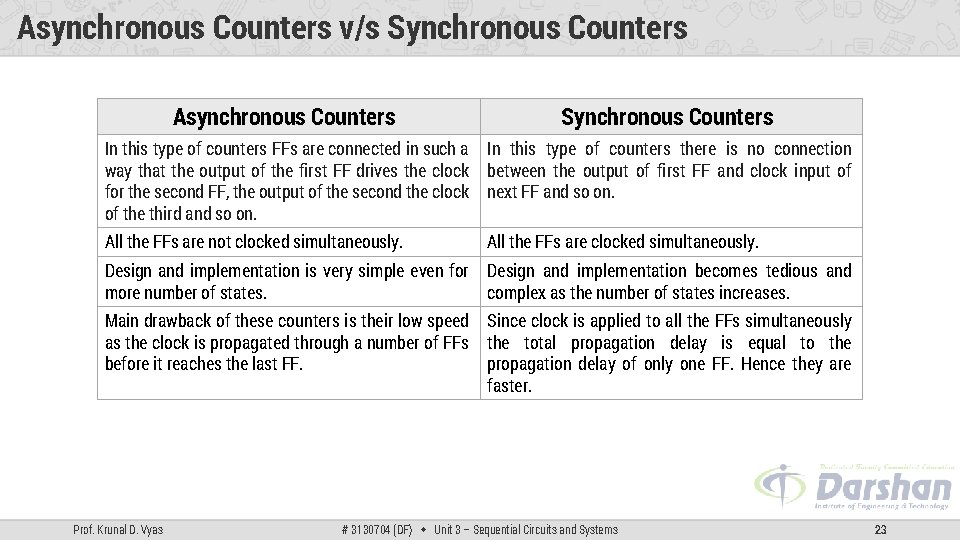
Asynchronous Counters v/s Synchronous Counters Asynchronous Counters Synchronous Counters In this type of counters FFs are connected in such a way that the output of the first FF drives the clock for the second FF, the output of the second the clock of the third and so on. In this type of counters there is no connection between the output of first FF and clock input of next FF and so on. All the FFs are not clocked simultaneously. All the FFs are clocked simultaneously. Design and implementation is very simple even for more number of states. Design and implementation becomes tedious and complex as the number of states increases. Main drawback of these counters is their low speed as the clock is propagated through a number of FFs before it reaches the last FF. Since clock is applied to all the FFs simultaneously the total propagation delay is equal to the propagation delay of only one FF. Hence they are faster. Prof. Krunal D. Vyas # 3130704 (DF) Unit 3 – Sequential Circuits and Systems 23

Section - 3

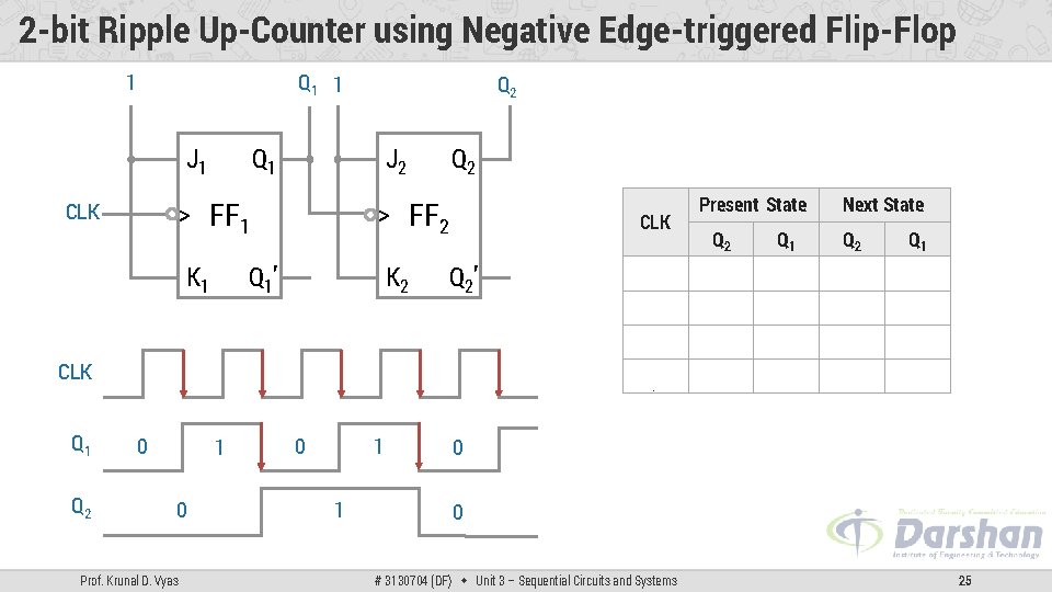
2 -bit Ripple Up-Counter using Negative Edge-triggered Flip-Flop 1 Q 1 J 1 CLK Q 2 J 2 > FF 1 > FF 2 K 1 K 2 Q 1’ CLK Q 2’ CLK Q 1 Q 2 0 1 0 Prof. Krunal D. Vyas 0 1 1 Present State Next State Q 2 Q 1 0 0 0 1 0 1 1 1 1 0 0 # 3130704 (DF) Unit 3 – Sequential Circuits and Systems 25

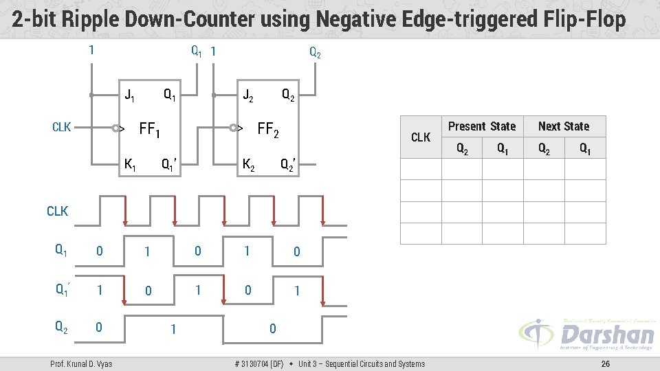
2 -bit Ripple Down-Counter using Negative Edge-triggered Flip-Flop Q 1 1 1 Q 1 J 1 > CLK Q 2 J 2 FF 1 K 1 Q 2 FF 2 > Q 1 ’ K 2 CLK Q 2 ’ CLK Q 1 0 1 0 Q 1 ’ 1 0 1 Q 2 0 Prof. Krunal D. Vyas 1 Present State Next State Q 2 Q 1 0 0 1 1 1 0 1 0 0 0 # 3130704 (DF) Unit 3 – Sequential Circuits and Systems 26

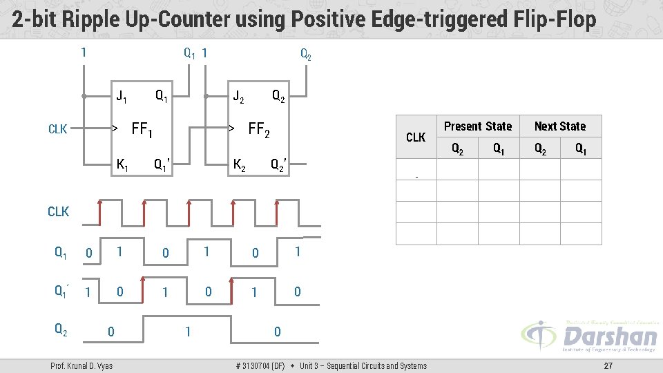
2 -bit Ripple Up-Counter using Positive Edge-triggered Flip-Flop 1 Q 1 J 1 > CLK K 1 Q 2 J 2 FF 1 FF 2 > Q 1 ’ K 2 CLK Q 2 ’ CLK Q 1 0 1 0 1 Q 1 ’ 1 0 1 0 Q 2 0 Prof. Krunal D. Vyas 1 Present State Next State Q 2 Q 1 0 0 0 1 0 1 1 1 1 0 0 0 # 3130704 (DF) Unit 3 – Sequential Circuits and Systems 27

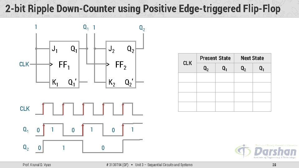
2 -bit Ripple Down-Counter using Positive Edge-triggered Flip-Flop 1 Q 1 1 Q 2 Q 1 J 1 > FF 1 CLK K 1 Q 2 J 2 > FF 2 Q 1’ K 2 CLK Q 2’ CLK Q 1 0 Q 2 0 Prof. Krunal D. Vyas 1 0 1 1 0 Present State Next State Q 2 Q 1 0 0 1 1 1 0 1 0 # 3130704 (DF) Unit 3 – Sequential Circuits and Systems 28

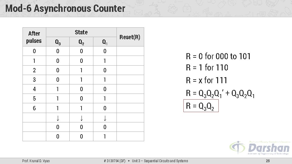
Mod-6 Asynchronous Counter State After pulses Q 3 Q 2 Q 1 0 0 0 1 0 2 0 1 0 0 3 0 1 1 0 4 1 0 0 0 5 1 0 6 1 1 0 1 ↓ ↓ ↓ 0 0 0 1 0 Prof. Krunal D. Vyas Reset(R) R = 0 for 000 to 101 R = 1 for 110 R = x for 111 R = Q 3 Q 2 Q 1’ + Q 3 Q 2 Q 1 R = Q 3 Q 2 # 3130704 (DF) Unit 3 – Sequential Circuits and Systems 29

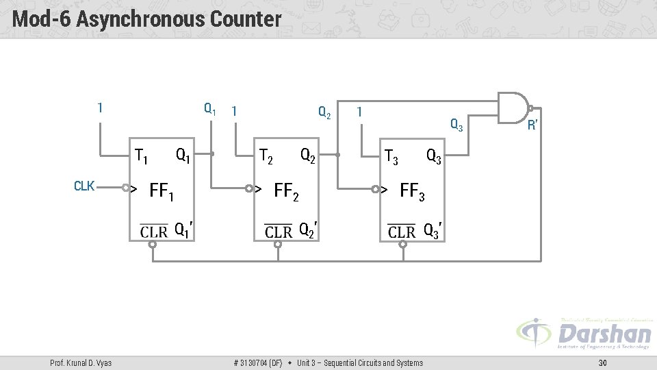
Mod-6 Asynchronous Counter 1 Q 1 T 1 CLK > FF 1 Q 1’ Prof. Krunal D. Vyas 1 Q 2 T 2 > FF 2 1 Q 3 R’ Q 3 T 3 > FF 3 Q 2’ # 3130704 (DF) Unit 3 – Sequential Circuits and Systems Q 3’ 30

Section - 4

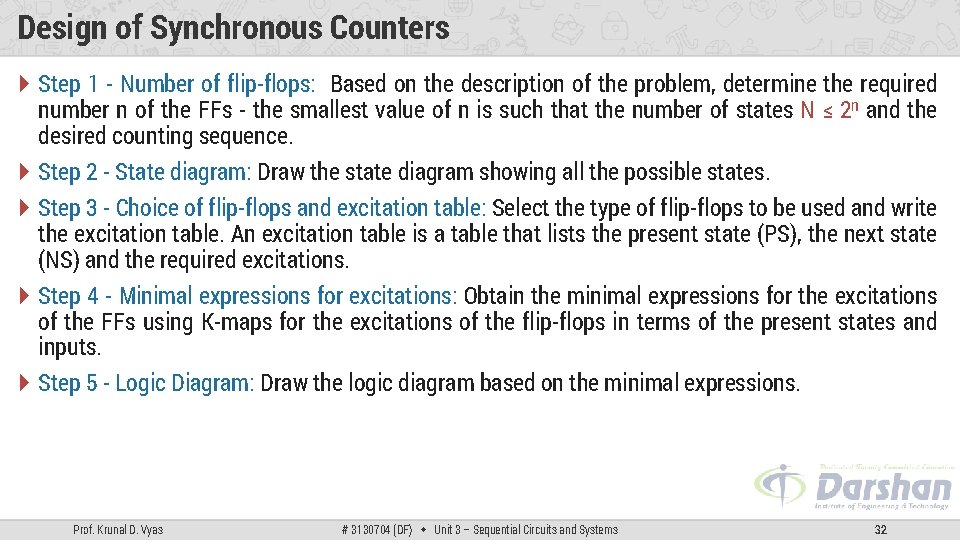
Design of Synchronous Counters Step 1 - Number of flip-flops: Based on the description of the problem, determine the required number n of the FFs - the smallest value of n is such that the number of states N ≤ 2 n and the desired counting sequence. Step 2 - State diagram: Draw the state diagram showing all the possible states. Step 3 - Choice of flip-flops and excitation table: Select the type of flip-flops to be used and write the excitation table. An excitation table is a table that lists the present state (PS), the next state (NS) and the required excitations. Step 4 - Minimal expressions for excitations: Obtain the minimal expressions for the excitations of the FFs using K-maps for the excitations of the flip-flops in terms of the present states and inputs. Step 5 - Logic Diagram: Draw the logic diagram based on the minimal expressions. Prof. Krunal D. Vyas # 3130704 (DF) Unit 3 – Sequential Circuits and Systems 32

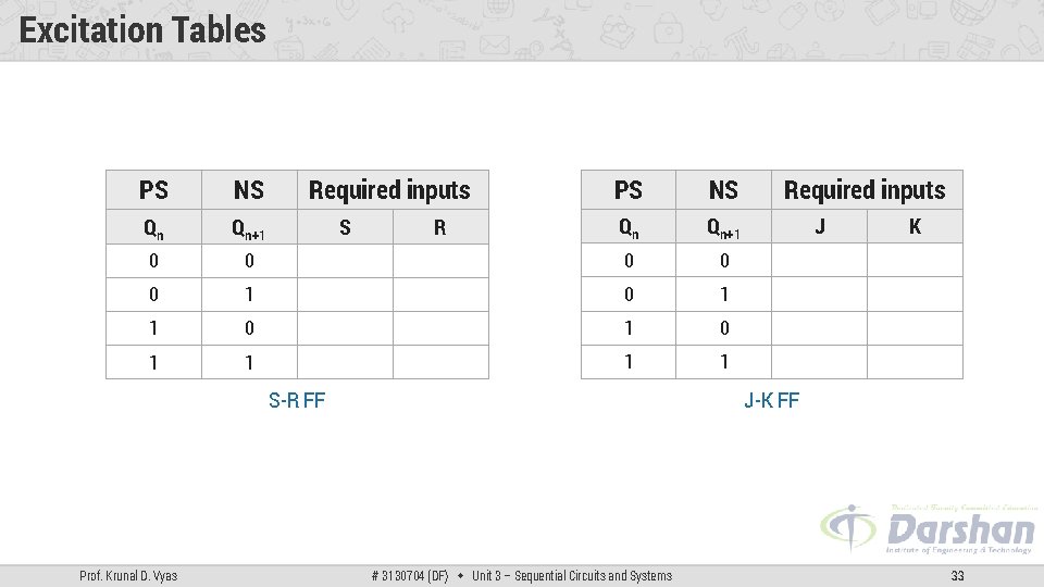
Excitation Tables PS NS R Qn Qn+1 J K 0 x 0 0 0 x 1 1 0 0 1 1 x 1 0 0 1 1 0 x 1 1 1 x 0 PS NS Required inputs Qn Qn+1 S 0 0 0 S-R FF Prof. Krunal D. Vyas Required inputs J-K FF # 3130704 (DF) Unit 3 – Sequential Circuits and Systems 33

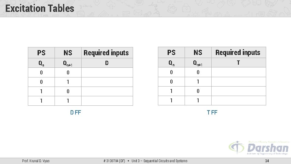
Excitation Tables PS NS Required inputs Qn Qn+1 D Qn Qn+1 T 0 0 0 0 1 1 1 1 0 D FF Prof. Krunal D. Vyas T FF # 3130704 (DF) Unit 3 – Sequential Circuits and Systems 34

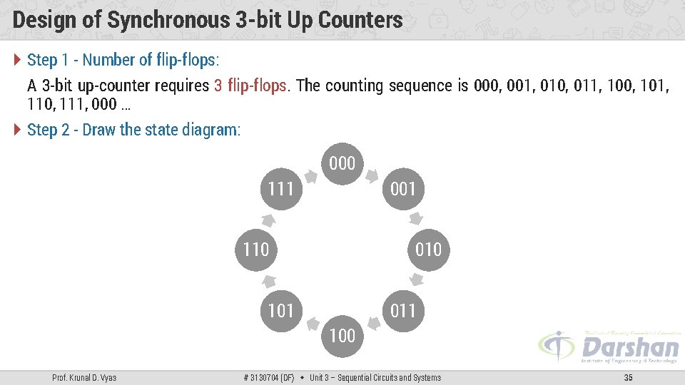
Design of Synchronous 3 -bit Up Counters Step 1 - Number of flip-flops: A 3 -bit up-counter requires 3 flip-flops. The counting sequence is 000, 001, 010, 011, 100, 101, 110, 111, 000 … Step 2 - Draw the state diagram: 000 111 001 110 010 101 011 100 Prof. Krunal D. Vyas # 3130704 (DF) Unit 3 – Sequential Circuits and Systems 35

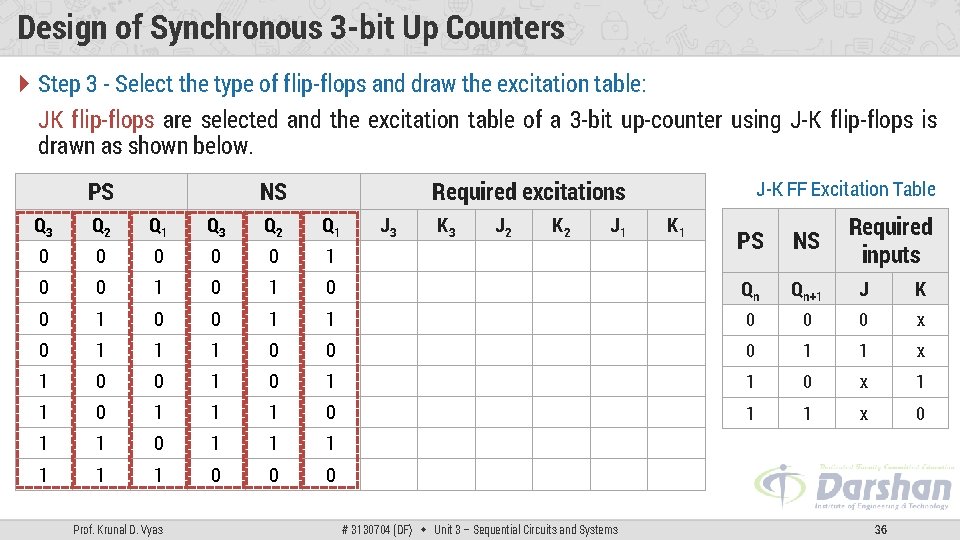
Design of Synchronous 3 -bit Up Counters Step 3 - Select the type of flip-flops and draw the excitation table: JK flip-flops are selected and the excitation table of a 3 -bit up-counter using J-K flip-flops is drawn as shown below. PS NS Required excitations J-K FF Excitation Table Q 3 Q 2 Q 1 J 3 K 3 J 2 K 2 J 1 K 1 0 0 0 1 0 x 1 x 0 0 1 0 0 x 1 x x 0 1 0 0 1 1 0 x x 0 0 1 1 1 0 0 1 x x 1 0 0 1 x 0 1 1 1 0 x 1 1 0 1 1 1 0 0 0 Prof. Krunal D. Vyas Required inputs PS NS 1 Qn Qn+1 J K 1 x 0 0 0 x 1 0 1 1 x 0 x 1 0 1 x x 1 1 1 x 0 x 0 1 x x 1 x 1 # 3130704 (DF) Unit 3 – Sequential Circuits and Systems 36

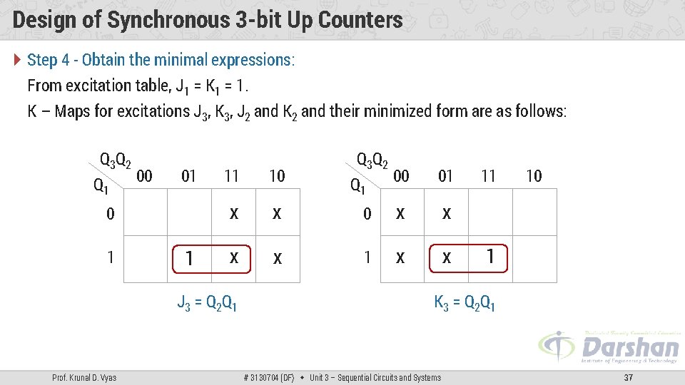
Design of Synchronous 3 -bit Up Counters Step 4 - Obtain the minimal expressions: From excitation table, J 1 = K 1 = 1. K – Maps for excitations J 3, K 3, J 2 and K 2 and their minimized form are as follows: Q 3 Q 2 00 Q 1 01 0 1 1 11 10 x x x x 1 x x J 3 = Q 2 Q 1 Prof. Krunal D. Vyas Q 3 Q 2 00 Q 1 01 11 10 1 K 3 = Q 2 Q 1 # 3130704 (DF) Unit 3 – Sequential Circuits and Systems 37

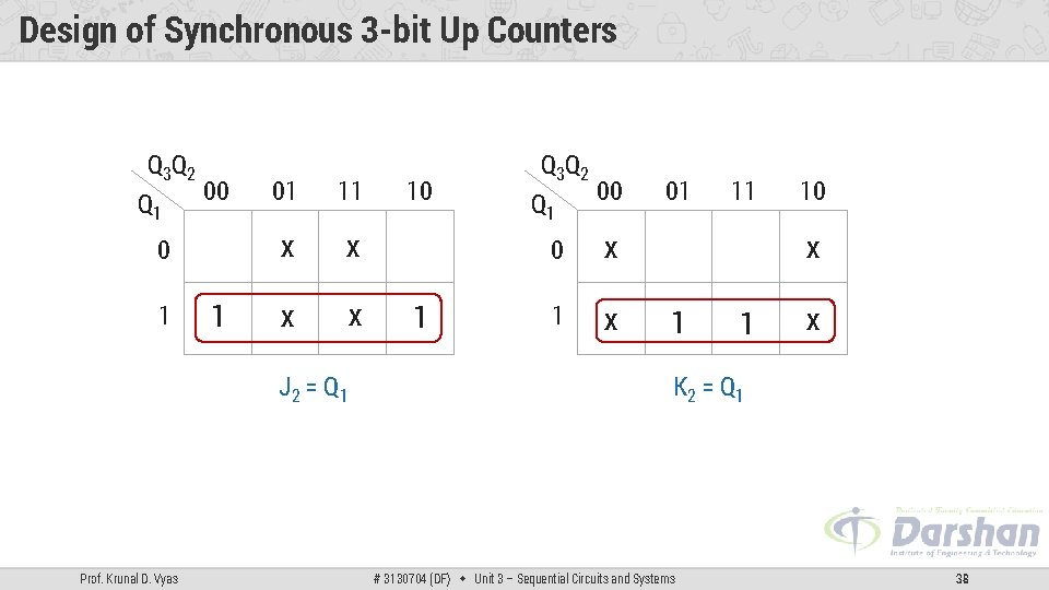
Design of Synchronous 3 -bit Up Counters Q 3 Q 2 00 Q 1 0 1 1 01 11 x x J 2 = Q 1 Prof. Krunal D. Vyas 10 1 Q 3 Q 2 00 Q 1 0 x 1 x 01 11 10 x 1 1 x K 2 = Q 1 # 3130704 (DF) Unit 3 – Sequential Circuits and Systems 38

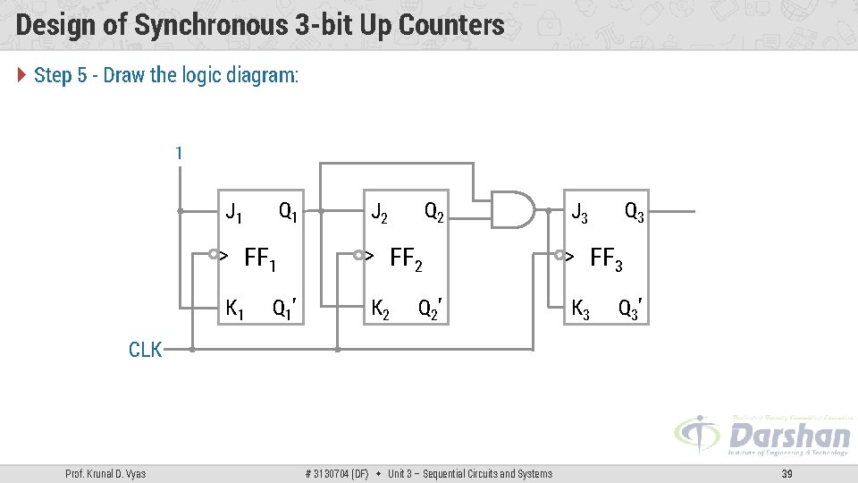
Design of Synchronous 3 -bit Up Counters Step 5 - Draw the logic diagram: 1 Q 1 J 1 Q 2 J 2 Q 3 J 3 > FF 1 > FF 2 > FF 3 K 1 K 2 K 3 Q 1’ Q 2’ Q 3’ CLK Prof. Krunal D. Vyas # 3130704 (DF) Unit 3 – Sequential Circuits and Systems 39

Section - 5

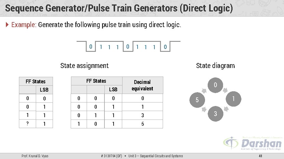
Sequence Generator/Pulse Train Generators (Direct Logic) Example: Generate the following pulse train using direct logic. 0 1 1 1 0 State assignment State diagram FF States LSB Decimal equivalent 0 0 0 0 1 1 0 1 1 3 ? 1 1 0 1 5 Prof. Krunal D. Vyas # 3130704 (DF) Unit 3 – Sequential Circuits and Systems 0 1 5 3 41

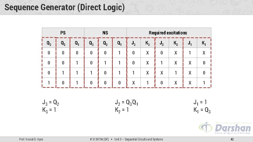
Sequence Generator (Direct Logic) PS Required excitations Q 3 Q 2 Q 1 J 3 K 3 J 2 K 2 J 1 K 1 0 0 0 1 0 X 1 X 0 0 1 1 0 X 1 X X 0 0 1 1 1 0 1 1 X X 1 X 0 1 0 0 0 X 1 0 X X 1 J 3 = Q 2 K 3 = 1 Prof. Krunal D. Vyas NS J 2 = Q 3’ Q 1 K 2 = 1 # 3130704 (DF) Unit 3 – Sequential Circuits and Systems J 1 = 1 K 1 = Q 3 42

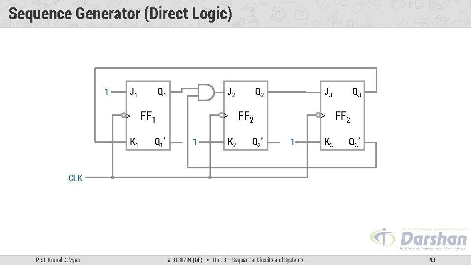
Sequence Generator (Direct Logic) 1 Q 1 J 1 > K 1 FF 1 Q 1 ’ Q 2 J 2 > 1 K 2 FF 2 Q 2 ’ Q 3 J 3 > 1 K 3 FF 2 Q 3 ’ CLK Prof. Krunal D. Vyas # 3130704 (DF) Unit 3 – Sequential Circuits and Systems 43

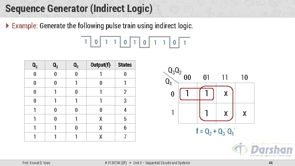
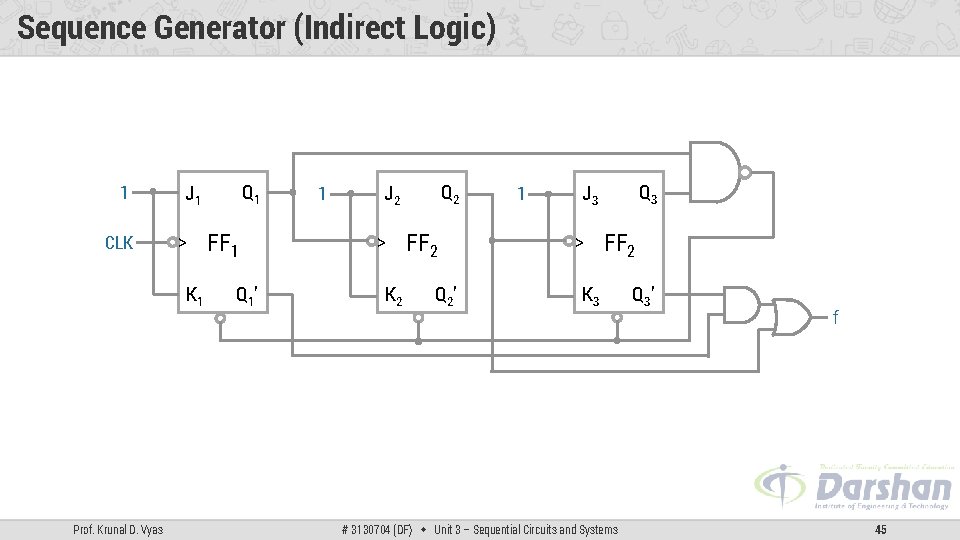
Sequence Generator (Indirect Logic) Example: Generate the following pulse train using indirect logic. 1 0 1 1 0 Q 3 Q 2 Q 1 Output(f) States 0 0 0 1 0 1 0 1 2 0 1 1 1 3 1 0 0 0 4 1 0 1 X 5 1 1 0 X 6 1 1 1 X 7 Prof. Krunal D. Vyas 1 0 1 Q 3 Q 2 00 Q 1 01 11 1 1 x 0 1 # 3130704 (DF) Unit 3 – Sequential Circuits and Systems 10 x f = Q 2 + Q 3’ Q 1’ 44

Sequence Generator (Indirect Logic) 1 CLK > K 1 Prof. Krunal D. Vyas Q 1 J 1 FF 1 Q 1 ’ 1 Q 2 J 2 > K 2 FF 2 Q 2 ’ 1 Q 3 J 3 > FF 2 K 3 # 3130704 (DF) Unit 3 – Sequential Circuits and Systems Q 3 ’ f 45