Digital Design Physical Implementation Chapter 7 Physical Implementation

- Slides: 33

Digital Design – Physical Implementation Chapter 7 Physical Implementation

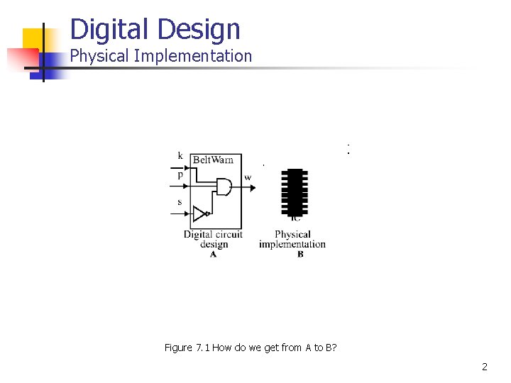
Digital Design Physical Implementation Figure 7. 1 How do we get from A to B? 2

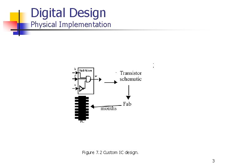
Digital Design Physical Implementation Figure 7. 2 Custom IC design. 3

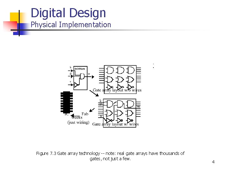
Digital Design Physical Implementation Figure 7. 3 Gate array technology -- note: real gate arrays have thousands of gates, not just a few. 4

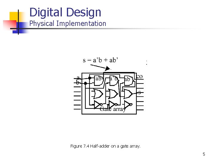
Digital Design Physical Implementation Figure 7. 4 Half-adder on a gate array. 5

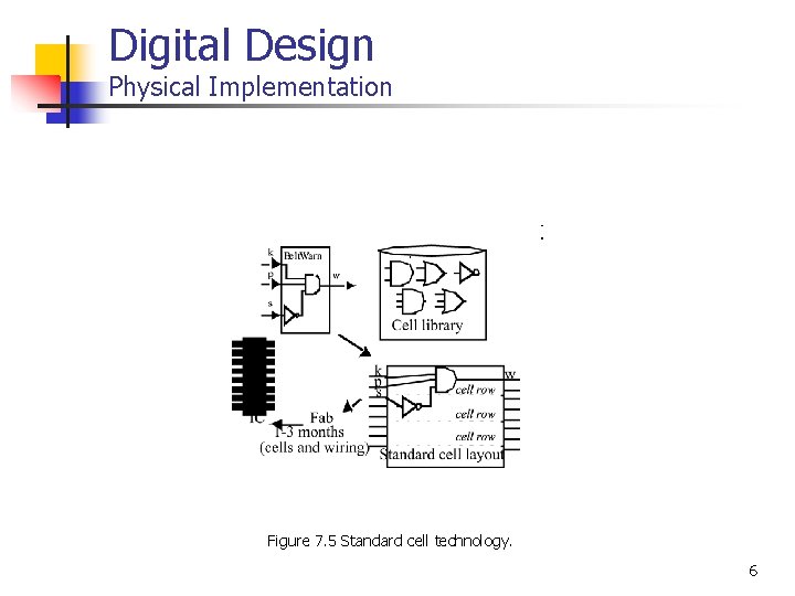
Digital Design Physical Implementation Figure 7. 5 Standard cell technology. 6

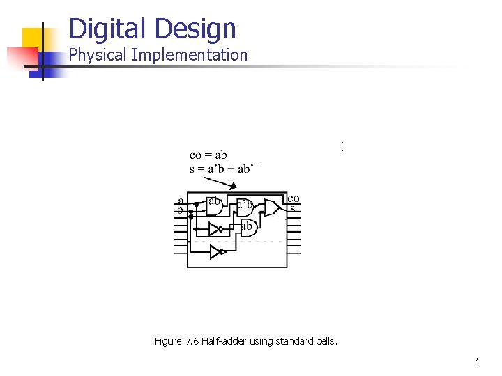
Digital Design Physical Implementation Figure 7. 6 Half-adder using standard cells. 7

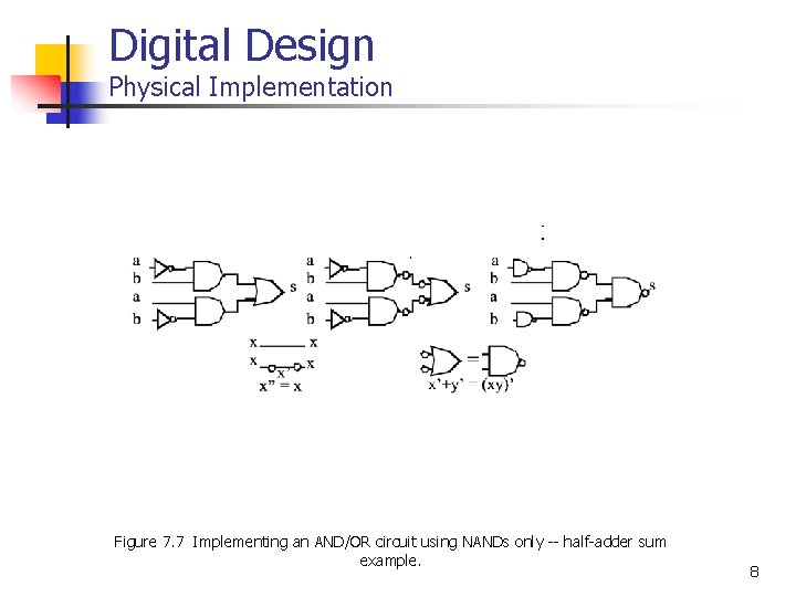
Digital Design Physical Implementation Figure 7. 7 Implementing an AND/OR circuit using NANDs only -- half-adder sum example. 8

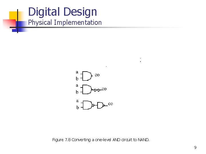
Digital Design Physical Implementation Figure 7. 8 Converting a one-level AND circuit to NAND. 9

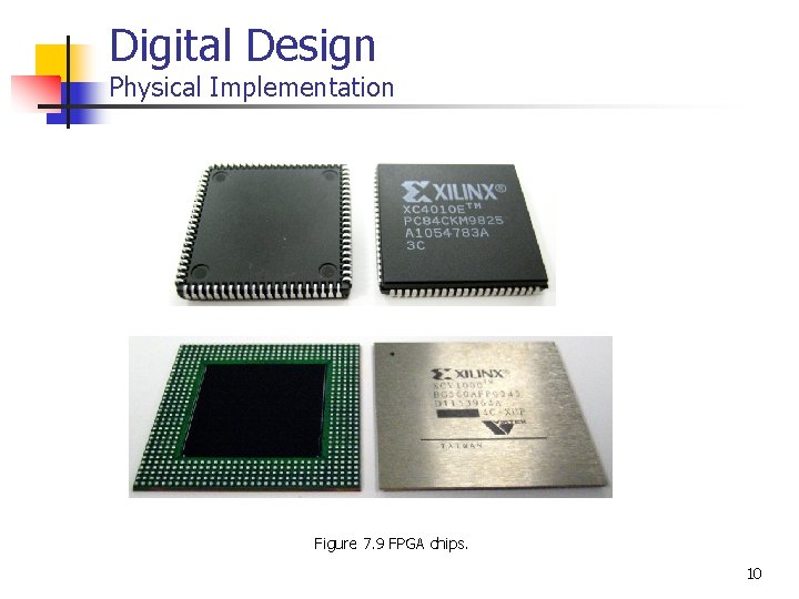
Digital Design Physical Implementation Figure 7. 9 FPGA chips. 10

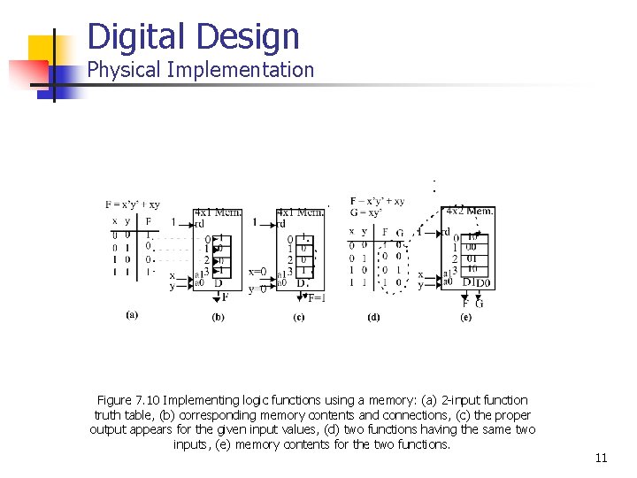
Digital Design Physical Implementation Figure 7. 10 Implementing logic functions using a memory: (a) 2 -input function truth table, (b) corresponding memory contents and connections, (c) the proper output appears for the given input values, (d) two functions having the same two inputs, (e) memory contents for the two functions. 11

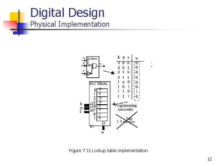
Digital Design Physical Implementation Figure 7. 11 Lookup table implementation. 12

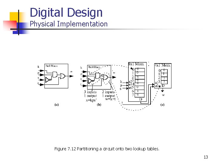
Digital Design Physical Implementation Figure 7. 12 Partitioning a circuit onto two lookup tables. 13

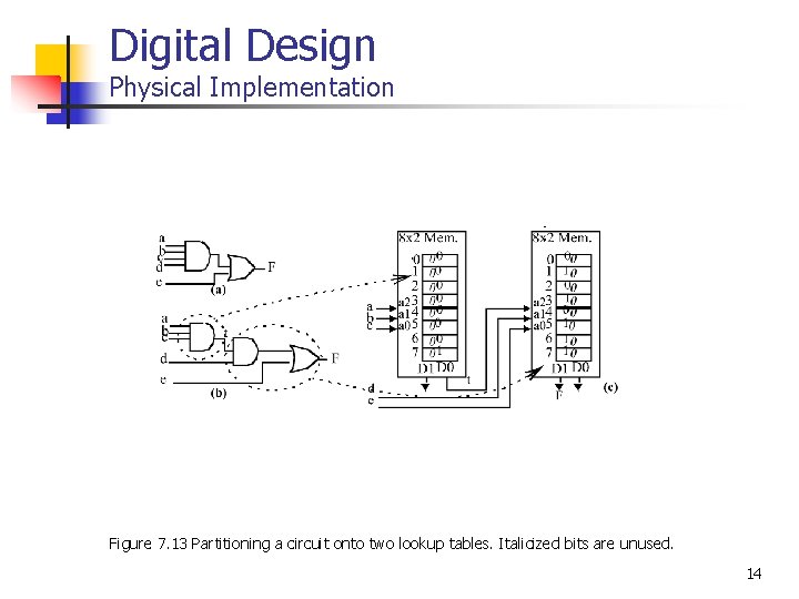
Digital Design Physical Implementation Figure 7. 13 Partitioning a circuit onto two lookup tables. Italicized bits are unused. 14

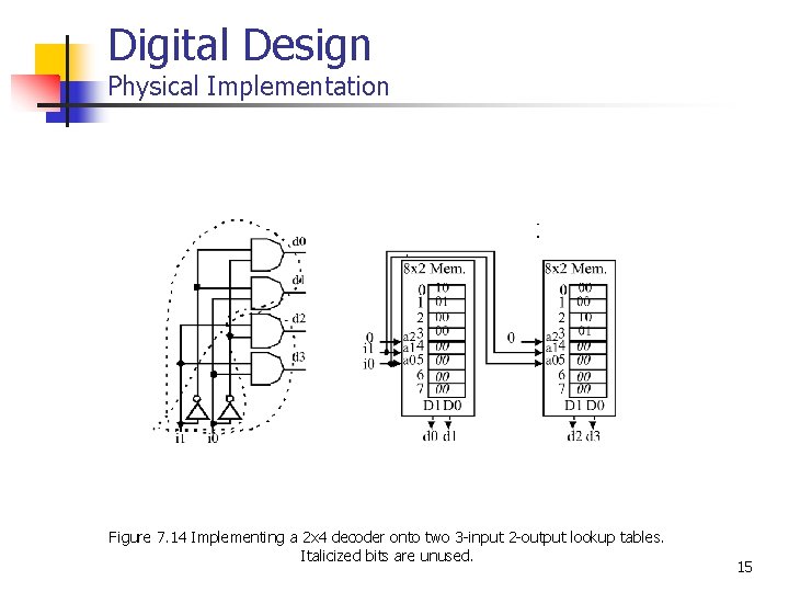
Digital Design Physical Implementation Figure 7. 14 Implementing a 2 x 4 decoder onto two 3 -input 2 -output lookup tables. Italicized bits are unused. 15

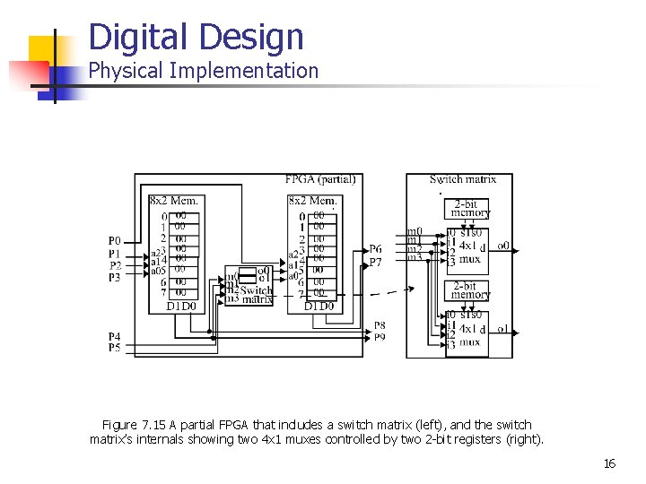
Digital Design Physical Implementation Figure 7. 15 A partial FPGA that includes a switch matrix (left), and the switch matrix’s internals showing two 4 x 1 muxes controlled by two 2 -bit registers (right). 16

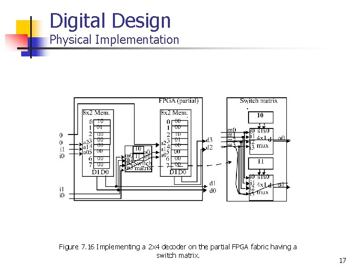
Digital Design Physical Implementation Figure 7. 16 Implementing a 2 x 4 decoder on the partial FPGA fabric having a switch matrix. 17

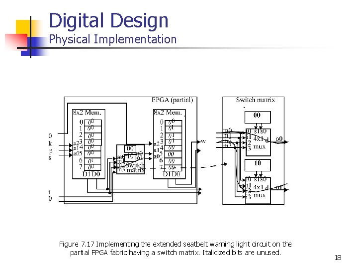
Digital Design Physical Implementation Figure 7. 17 Implementing the extended seatbelt warning light circuit on the partial FPGA fabric having a switch matrix. Italicized bits are unused. 18

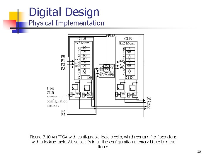
Digital Design Physical Implementation Figure 7. 18 An FPGA with configurable logic blocks, which contain flip-flops along with a lookup table. We’ve put 0 s in all the configuration memory bit cells in the figure. 19

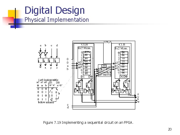
Digital Design Physical Implementation Figure 7. 19 Implementing a sequential circuit on an FPGA. 20

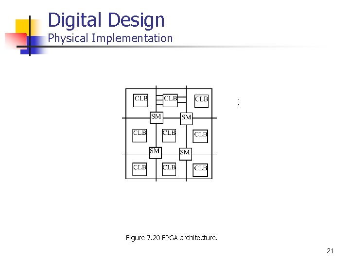
Digital Design Physical Implementation Figure 7. 20 FPGA architecture. 21

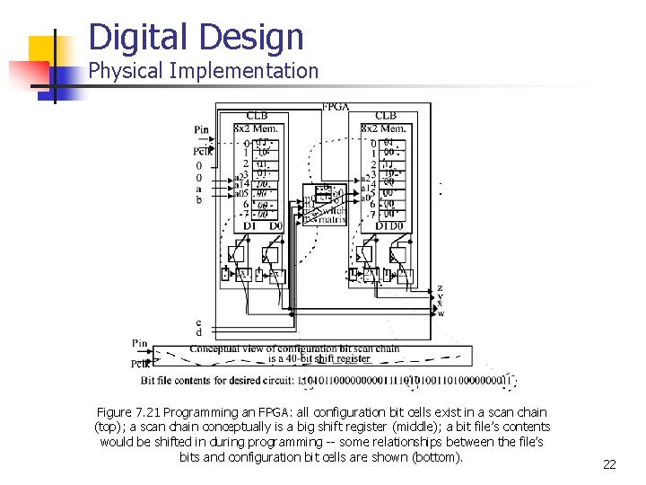
Digital Design Physical Implementation Figure 7. 21 Programming an FPGA: all configuration bit cells exist in a scan chain (top); a scan chain conceptually is a big shift register (middle); a bit file’s contents would be shifted in during programming -- some relationships between the file’s bits and configuration bit cells are shown (bottom). 22

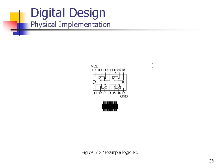
Digital Design Physical Implementation Figure 7. 22 Example logic IC. 23

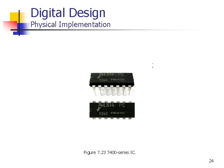
Digital Design Physical Implementation Figure 7. 23 7400 -series IC. 24

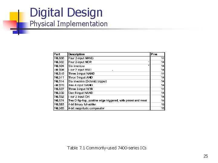
Digital Design Physical Implementation Table 7. 1 Commonly-used 7400 -series ICs 25

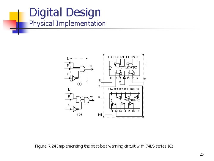
Digital Design Physical Implementation Figure 7. 24 Implementing the seat-belt warning circuit with 74 LS series ICs. 26

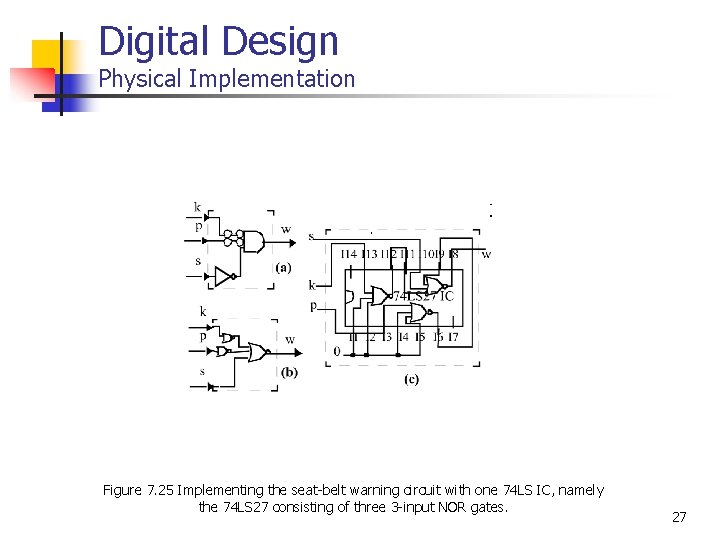
Digital Design Physical Implementation Figure 7. 25 Implementing the seat-belt warning circuit with one 74 LS IC, namely the 74 LS 27 consisting of three 3 -input NOR gates. 27

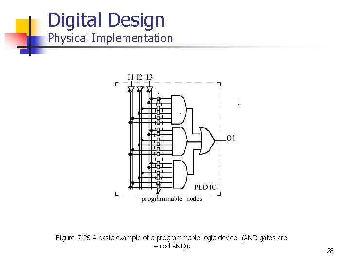
Digital Design Physical Implementation Figure 7. 26 A basic example of a programmable logic device. (AND gates are wired-AND). 28

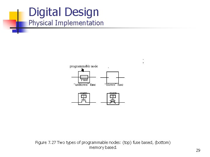
Digital Design Physical Implementation Figure 7. 27 Two types of programmable nodes: (top) fuse based, (bottom) memory based. 29

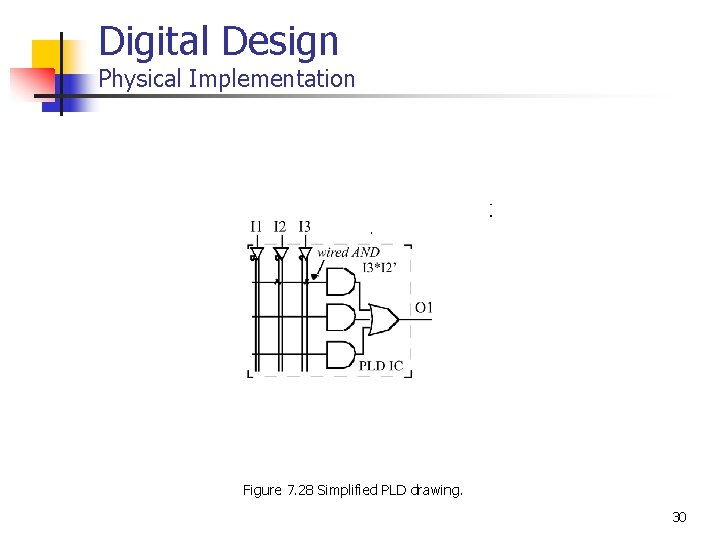
Digital Design Physical Implementation Figure 7. 28 Simplified PLD drawing. 30

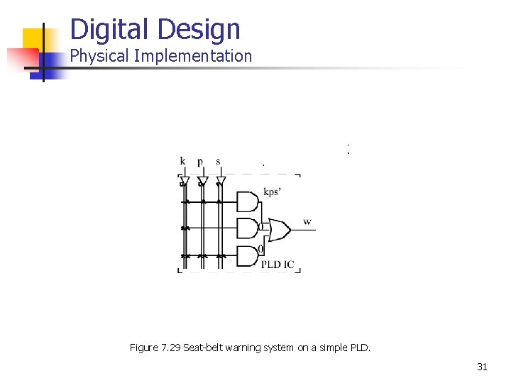
Digital Design Physical Implementation Figure 7. 29 Seat-belt warning system on a simple PLD. 31

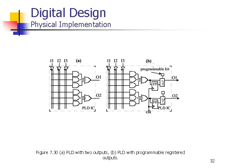
Digital Design Physical Implementation Figure 7. 30 (a) PLD with two outputs, (b) PLD with programmable registered outputs. 32

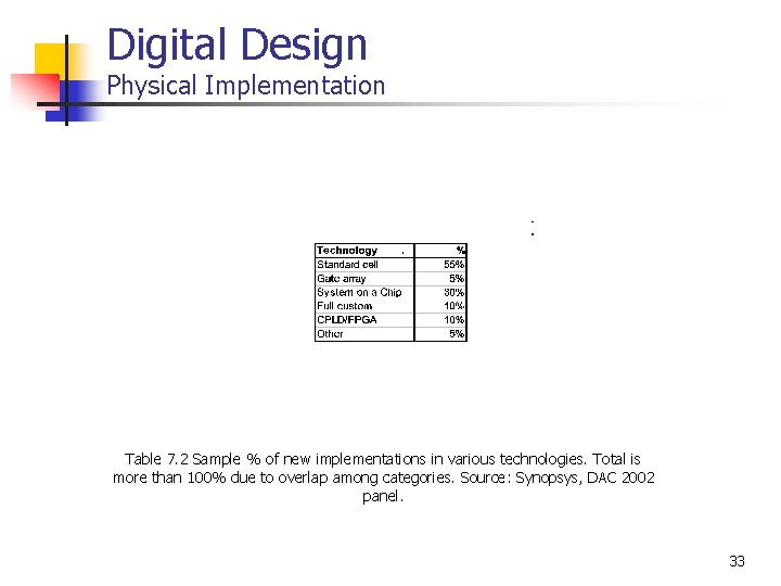
Digital Design Physical Implementation Table 7. 2 Sample % of new implementations in various technologies. Total is more than 100% due to overlap among categories. Source: Synopsys, DAC 2002 panel. 33