Digital Design Datapath Components Chapter 4 Datapath Components

- Slides: 74

Digital Design – Datapath Components Chapter 4 Datapath Components

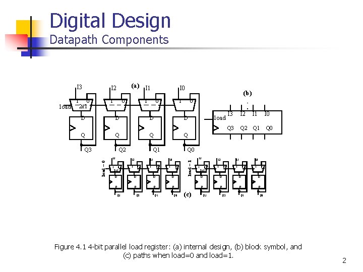
Digital Design Datapath Components I 2 1 1 0 2 x 1 (a) I 1 0 I 0 1 0 (b) 1 0 D D Q Q Q 2 load = 0 Q 3 Q 1 I 3 I 2 1 1 0 2 x 1 I 1 0 I 0 1 0 D D Q Q Q 3 Q 2 Q 1 load I 3 I 2 I 1 I 0 Q 3 Q 2 Q 1 Q 0 Q 0 load = 1 load I 3 (c) I 3 I 2 1 1 0 2 x 1 I 1 0 I 0 1 0 D D Q Q Q 3 Q 2 Q 1 Q 0 Figure 4. 1 4 -bit parallel load register: (a) internal design, (b) block symbol, and (c) paths when load=0 and load=1. 2

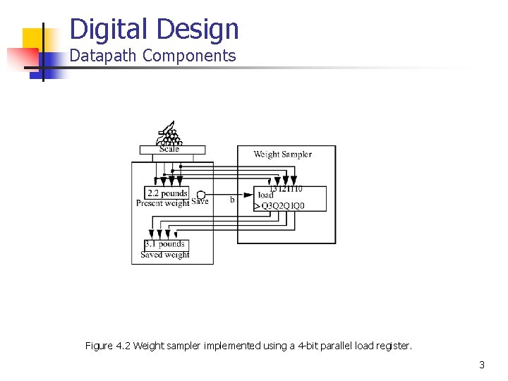
Digital Design Datapath Components Figure 4. 2 Weight sampler implemented using a 4 -bit parallel load register. 3

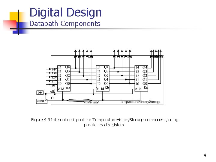
Digital Design Datapath Components Figure 4. 3 Internal design of the Temperature. History. Storage component, using parallel load registers. 4

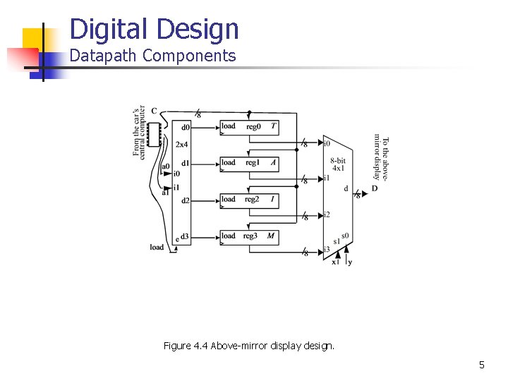
Digital Design Datapath Components Figure 4. 4 Above-mirror display design. 5

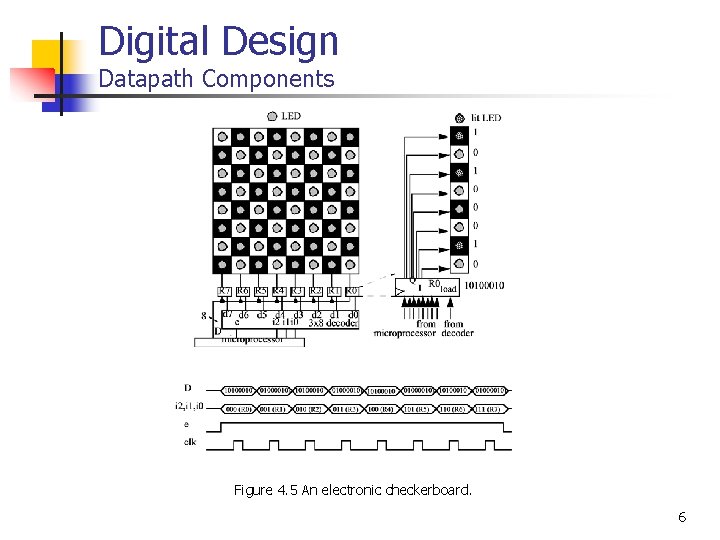
Digital Design Datapath Components Figure 4. 5 An electronic checkerboard. 6

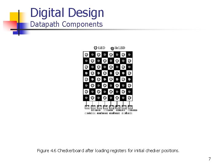
Digital Design Datapath Components Figure 4. 6 Checkerboard after loading registers for initial checker positions. 7

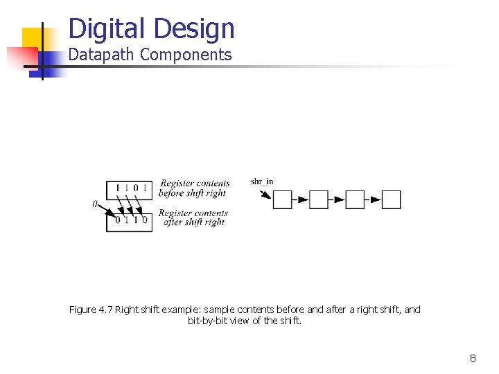
Digital Design Datapath Components Figure 4. 7 Right shift example: sample contents before and after a right shift, and bit-by-bit view of the shift. 8

Digital Design Datapath Components Figure 4. 8 Shift register: (a) implementation, (b) paths when shr=1, and (c) register symbol. 9

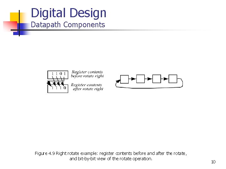
Digital Design Datapath Components Figure 4. 9 Right rotate example: register contents before and after the rotate, and bit-by-bit view of the rotate operation. 10

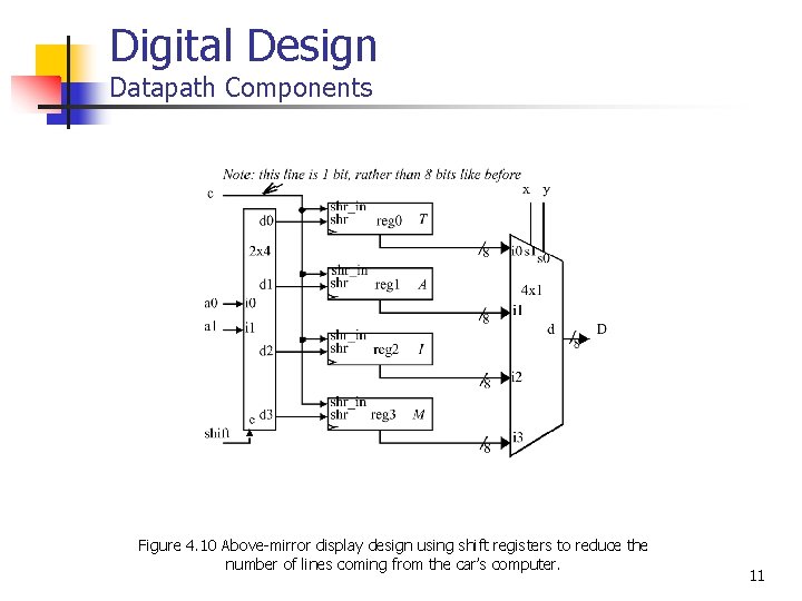
Digital Design Datapath Components Figure 4. 10 Above-mirror display design using shift registers to reduce the number of lines coming from the car’s computer. 11

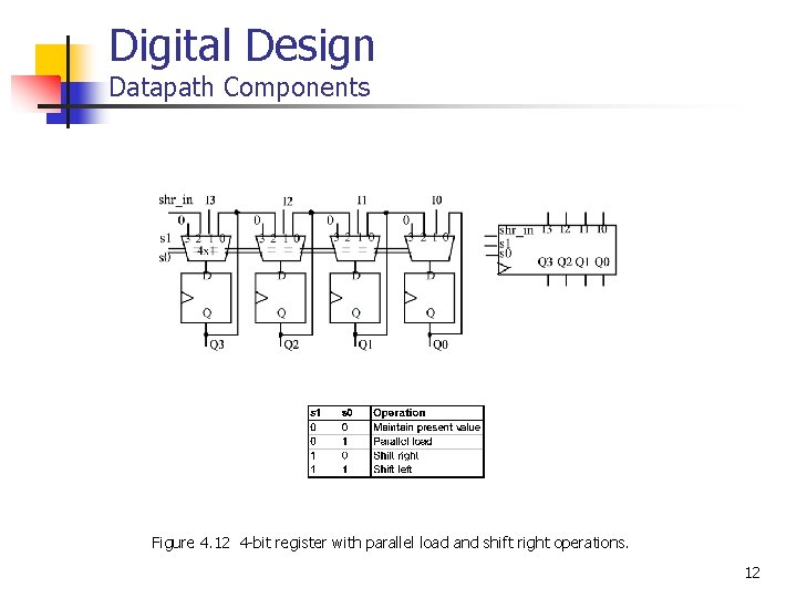
Digital Design Datapath Components Figure 4. 12 4 -bit register with parallel load and shift right operations. 12

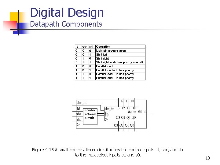
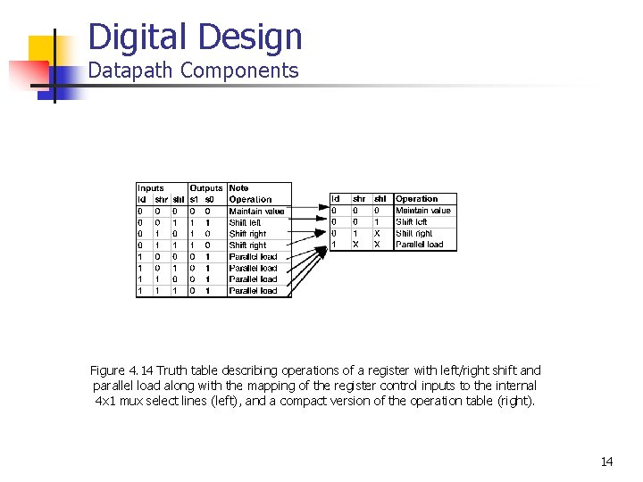
Digital Design Datapath Components Figure 4. 13 A small combinational circuit maps the control inputs ld, shr, and shl to the mux select inputs s 1 and s 0. 13

Digital Design Datapath Components Figure 4. 14 Truth table describing operations of a register with left/right shift and parallel load along with the mapping of the register control inputs to the internal 4 x 1 mux select lines (left), and a compact version of the operation table (right). 14

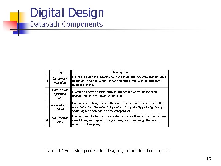
Digital Design Datapath Components Table 4. 1 Four-step process for designing a multifunction register. 15

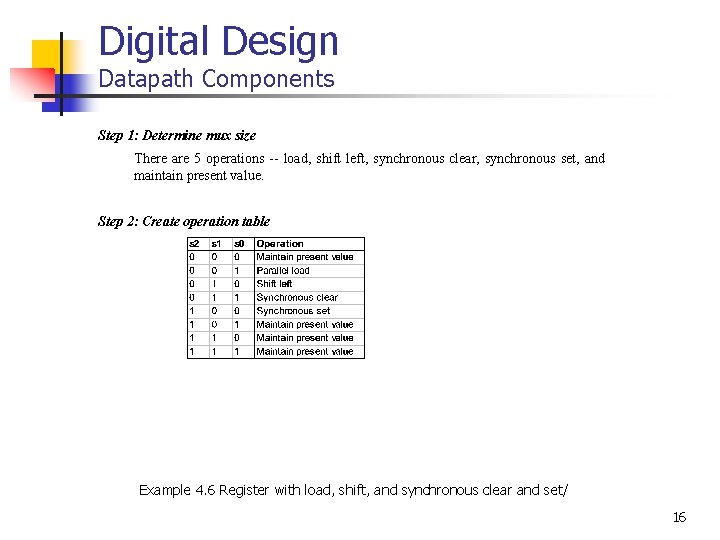
Digital Design Datapath Components Step 1: Determine mux size There are 5 operations -- load, shift left, synchronous clear, synchronous set, and maintain present value. Step 2: Create operation table Example 4. 6 Register with load, shift, and synchronous clear and set/ 16

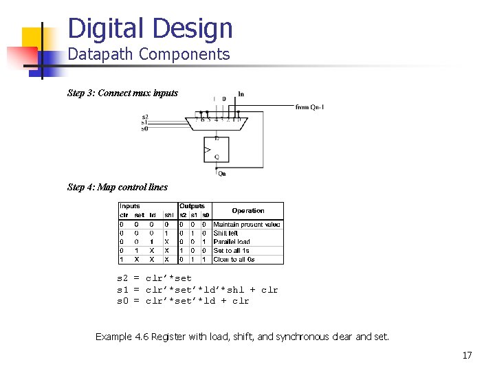
Digital Design Datapath Components Step 3: Connect mux inputs Step 4: Map control lines s 2 = clr’*set s 1 = clr’*set’*ld’*shl + clr s 0 = clr’*set’*ld + clr Example 4. 6 Register with load, shift, and synchronous clear and set. 17

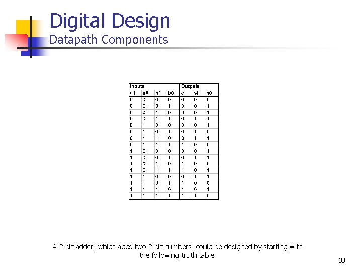
Digital Design Datapath Components A 2 -bit adder, which adds two 2 -bit numbers, could be designed by starting with the following truth table. 18

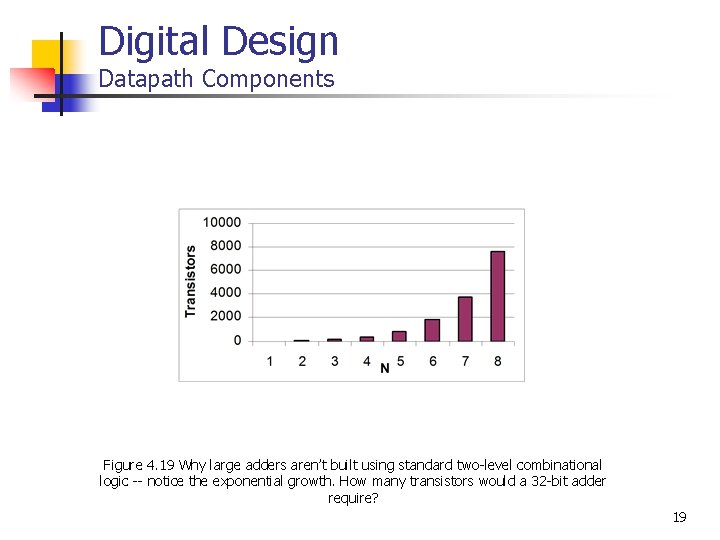
Digital Design Datapath Components Figure 4. 19 Why large adders aren’t built using standard two-level combinational logic -- notice the exponential growth. How many transistors would a 32 -bit adder require? 19

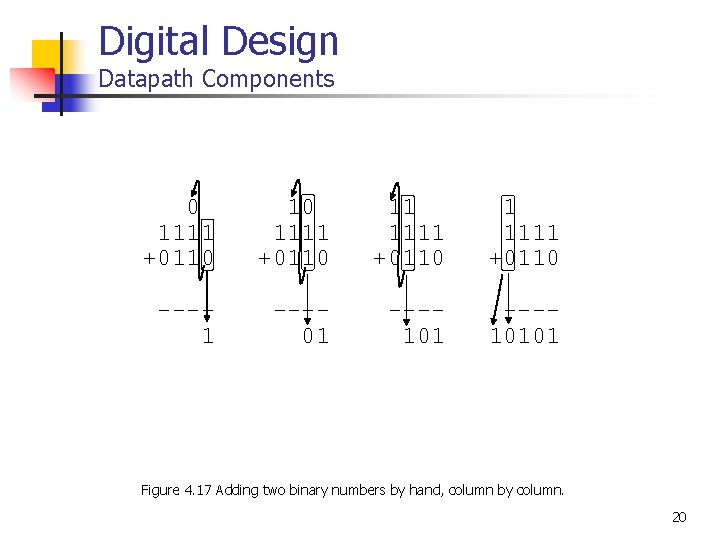
Digital Design Datapath Components 0 1111 +0110 11 1111 +0110 ---1 ---01 ---10101 Figure 4. 17 Adding two binary numbers by hand, column by column. 20

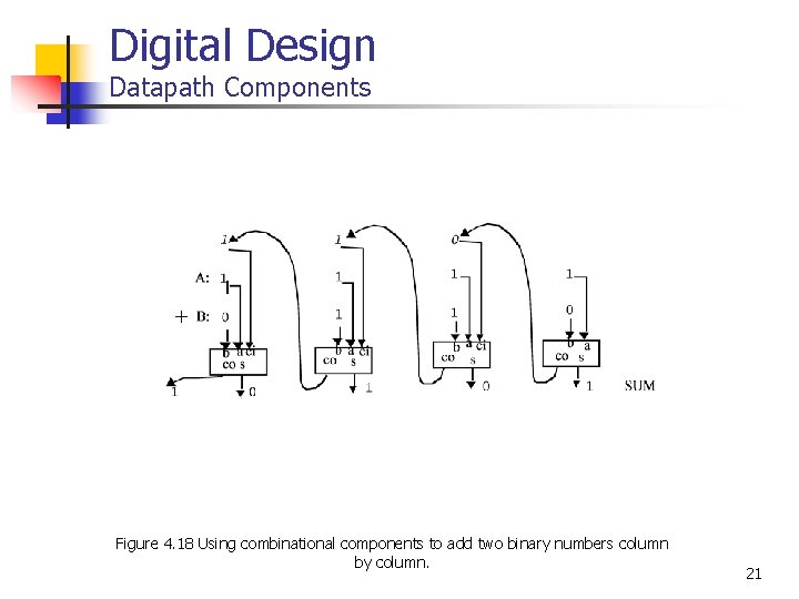
Digital Design Datapath Components Figure 4. 18 Using combinational components to add two binary numbers column by column. 21

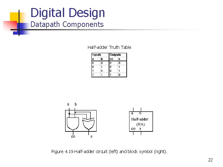
Digital Design Datapath Components Half-adder Truth Table Figure 4. 19 Half-adder circuit (left) and block symbol (right). 22

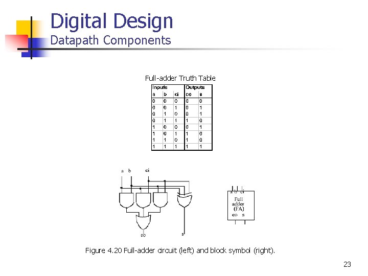
Digital Design Datapath Components Full-adder Truth Table Figure 4. 20 Full-adder circuit (left) and block symbol (right). 23

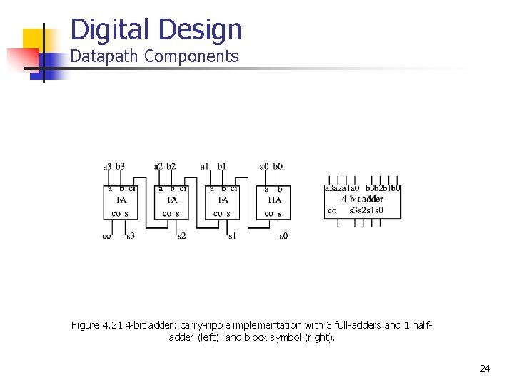
Digital Design Datapath Components Figure 4. 21 4 -bit adder: carry-ripple implementation with 3 full-adders and 1 halfadder (left), and block symbol (right). 24

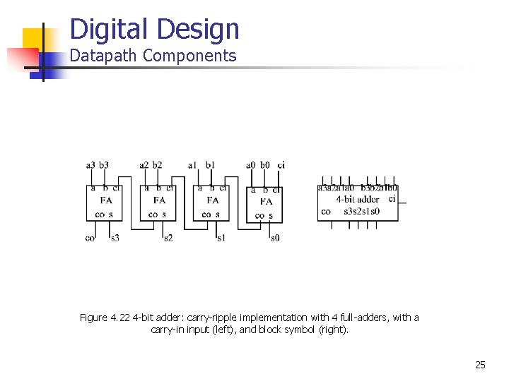
Digital Design Datapath Components Figure 4. 22 4 -bit adder: carry-ripple implementation with 4 full-adders, with a carry-in input (left), and block symbol (right). 25

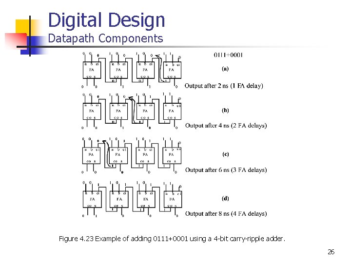
Digital Design Datapath Components Figure 4. 23 Example of adding 0111+0001 using a 4 -bit carry-ripple adder. 26

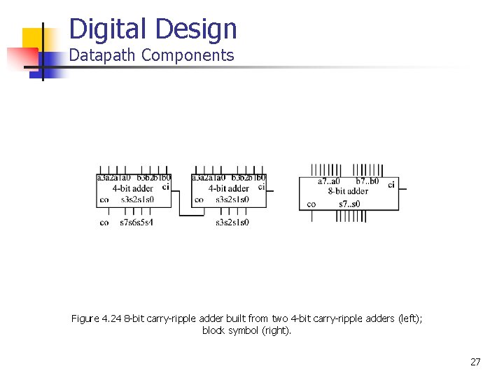
Digital Design Datapath Components Figure 4. 24 8 -bit carry-ripple adder built from two 4 -bit carry-ripple adders (left); block symbol (right). 27

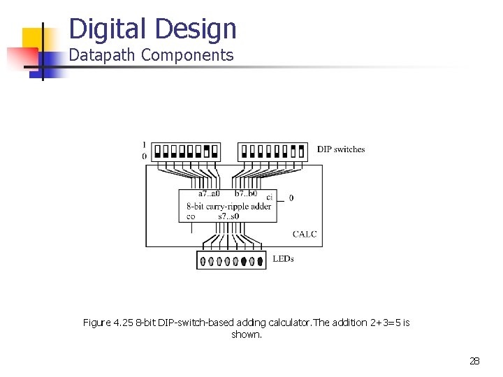
Digital Design Datapath Components Figure 4. 25 8 -bit DIP-switch-based adding calculator. The addition 2+3=5 is shown. 28

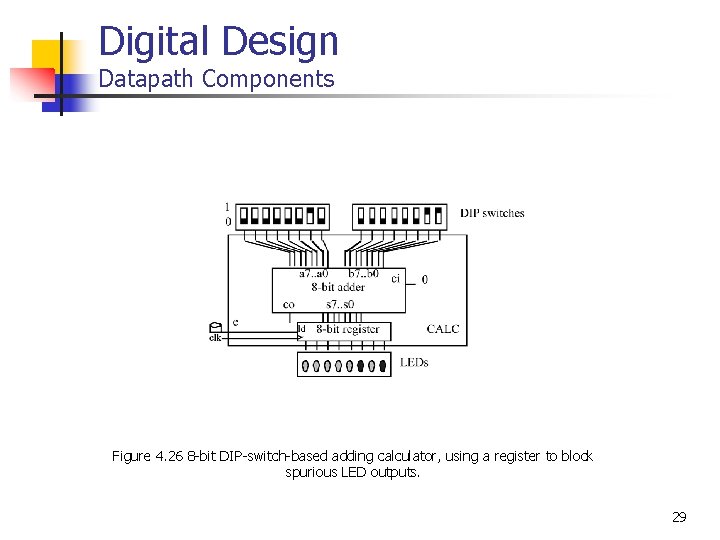
Digital Design Datapath Components Figure 4. 26 8 -bit DIP-switch-based adding calculator, using a register to block spurious LED outputs. 29

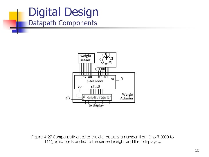
Digital Design Datapath Components Figure 4. 27 Compensating scale: the dial outputs a number from 0 to 7 (000 to 111), which gets added to the sensed weight and then displayed. 30

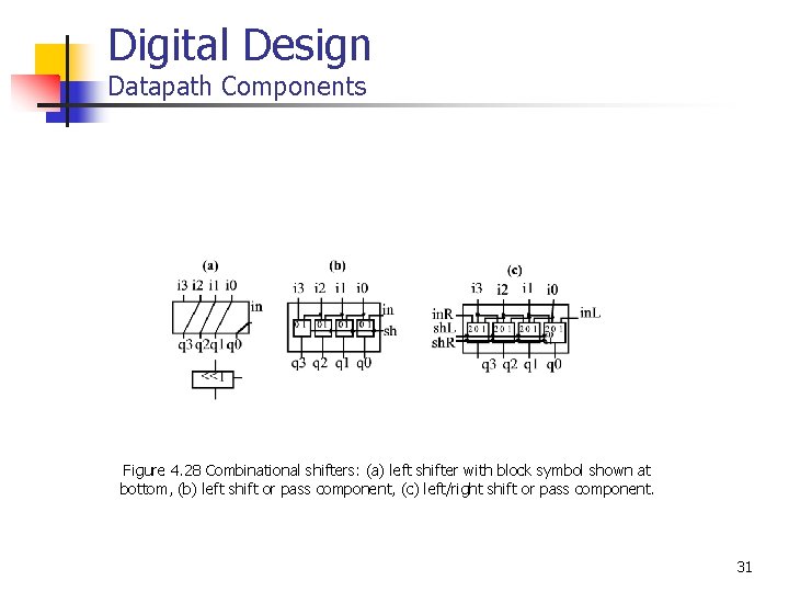
Digital Design Datapath Components Figure 4. 28 Combinational shifters: (a) left shifter with block symbol shown at bottom, (b) left shift or pass component, (c) left/right shift or pass component. 31

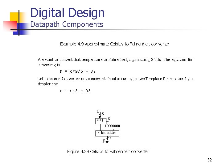
Digital Design Datapath Components Example 4. 9 Approximate Celsius to Fahrenheit converter. We want to convert that temperature to Fahrenheit, again using 8 bits. The equation for converting is: F = C*9/5 + 32 Let’s assume that we are not concerned about accuracy, so we’ll replace the equation by a simpler one: F = C*2 + 32 Figure 4. 29 Celsius to Fahrenheit converter. 32

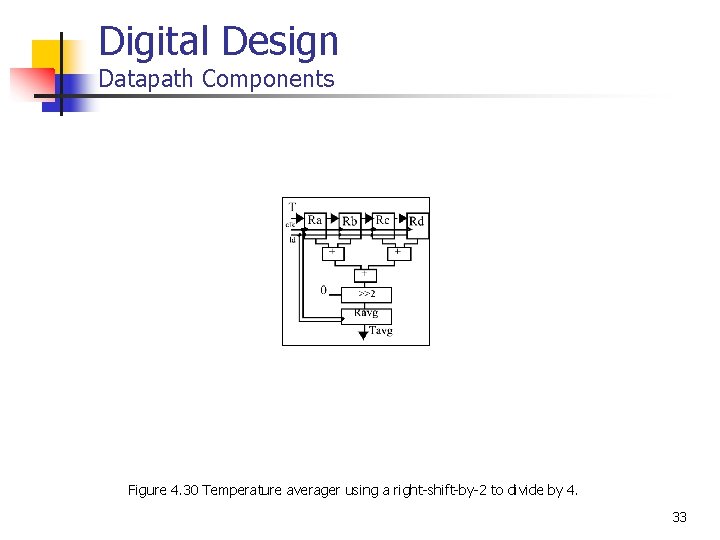
Digital Design Datapath Components Figure 4. 30 Temperature averager using a right-shift-by-2 to divide by 4. 33

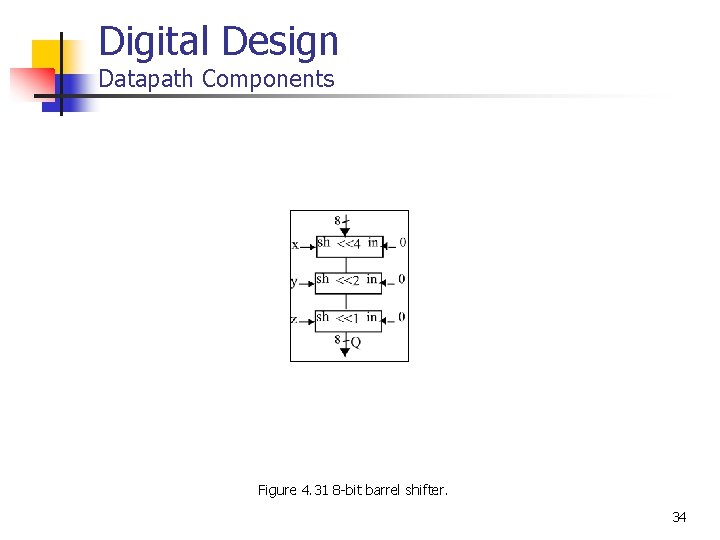
Digital Design Datapath Components Figure 4. 31 8 -bit barrel shifter. 34

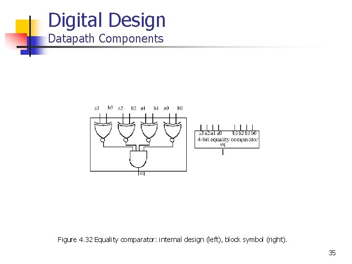
Digital Design Datapath Components Figure 4. 32 Equality comparator: internal design (left), block symbol (right). 35

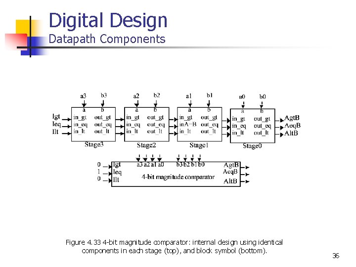
Digital Design Datapath Components Figure 4. 33 4 -bit magnitude comparator: internal design using identical components in each stage (top), and block symbol (bottom). 36

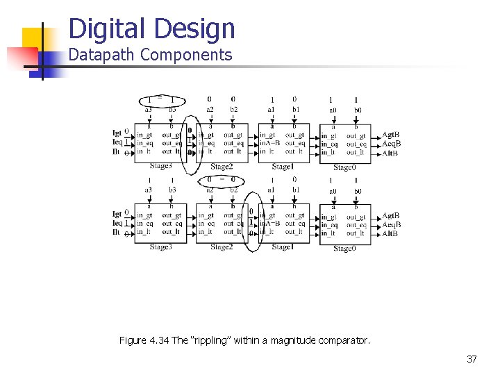
Digital Design Datapath Components Figure 4. 34 The “rippling” within a magnitude comparator. 37

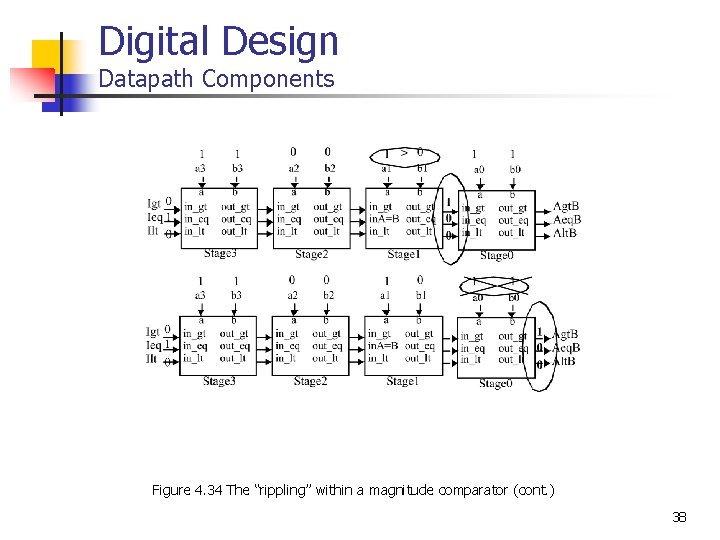
Digital Design Datapath Components Figure 4. 34 The “rippling” within a magnitude comparator (cont. ) 38

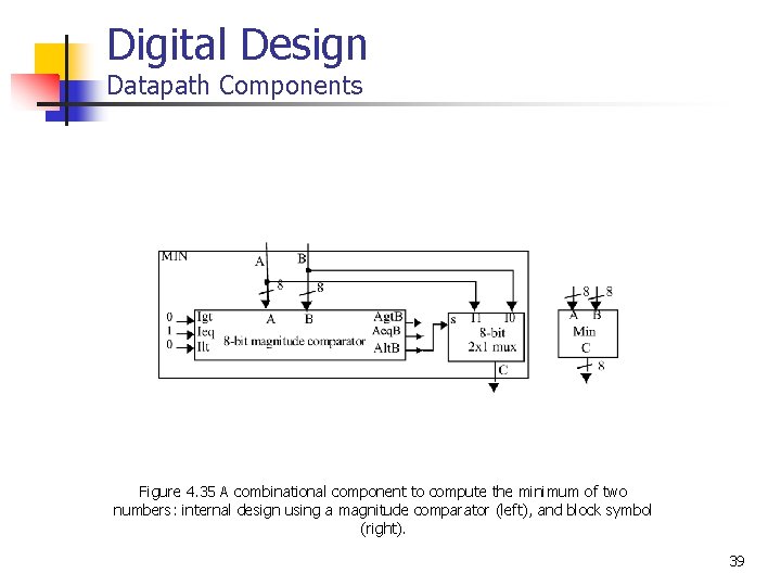
Digital Design Datapath Components Figure 4. 35 A combinational component to compute the minimum of two numbers: internal design using a magnitude comparator (left), and block symbol (right). 39

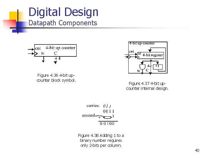
Digital Design Datapath Components Figure 4. 36 4 -bit upcounter block symbol. Figure 4. 37 4 -bit upcounter internal design. Figure 4. 38 Adding 1 to a binary number requires only 2 -bits per column. 40

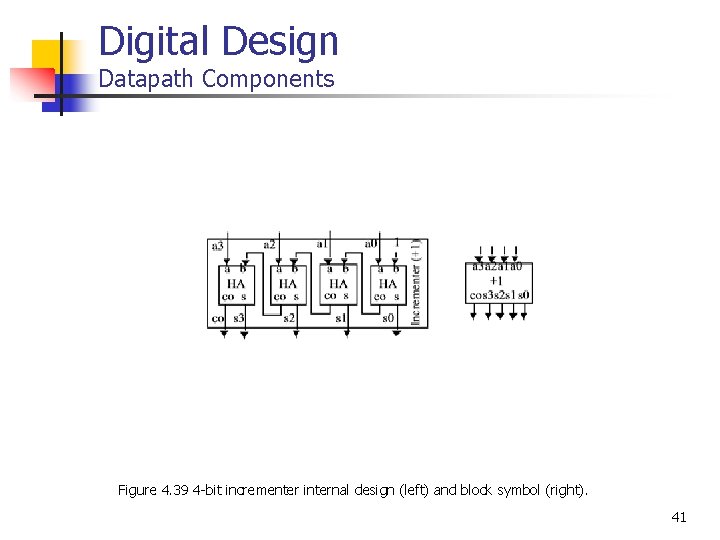
Digital Design Datapath Components Figure 4. 39 4 -bit incrementer internal design (left) and block symbol (right). 41

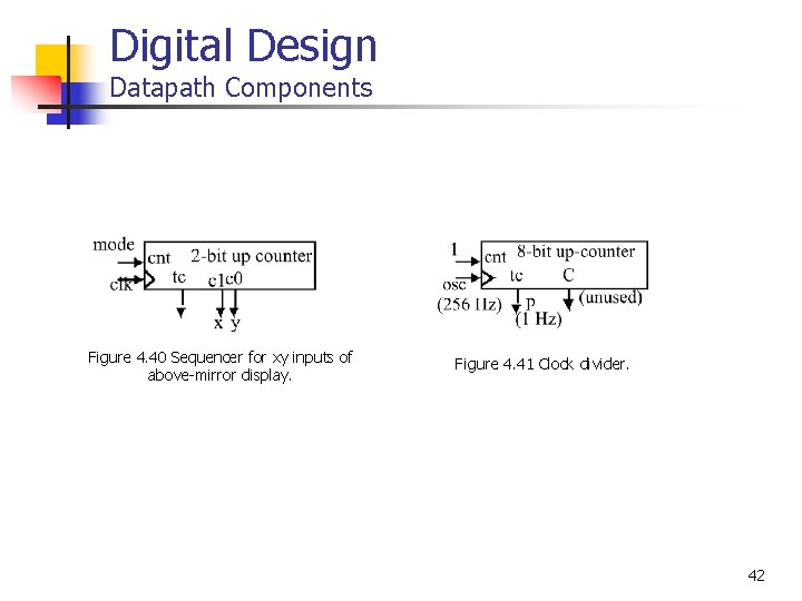
Digital Design Datapath Components Figure 4. 40 Sequencer for xy inputs of above-mirror display. Figure 4. 41 Clock divider. 42

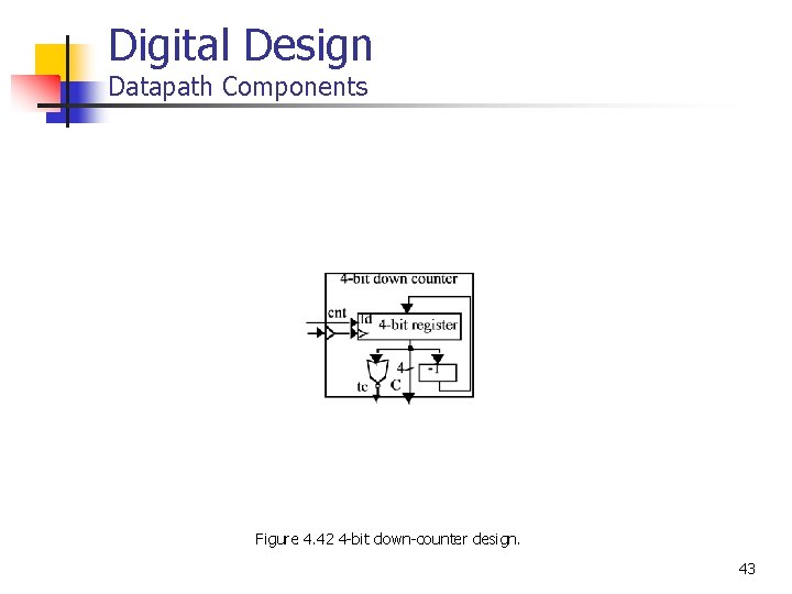
Digital Design Datapath Components Figure 4. 42 4 -bit down-counter design. 43

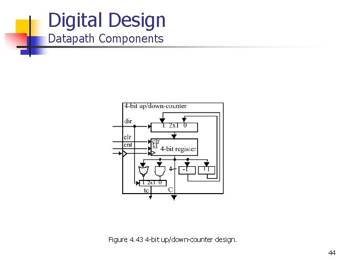
Digital Design Datapath Components Figure 4. 43 4 -bit up/down-counter design. 44

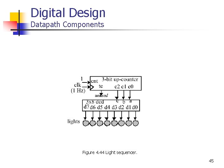
Digital Design Datapath Components Figure 4. 44 Light sequencer. 45

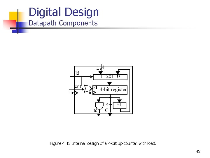
Digital Design Datapath Components Figure 4. 45 Internal design of a 4 -bit up-counter with load. 46

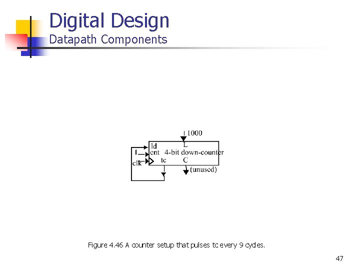
Digital Design Datapath Components Figure 4. 46 A counter setup that pulses tc every 9 cycles. 47

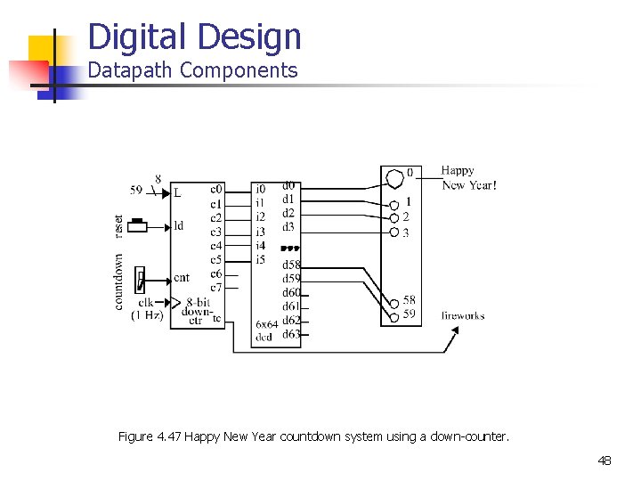
Digital Design Datapath Components Figure 4. 47 Happy New Year countdown system using a down-counter. 48

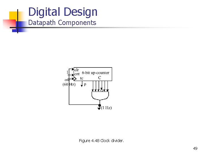
Digital Design Datapath Components Figure 4. 48 Clock divider. 49

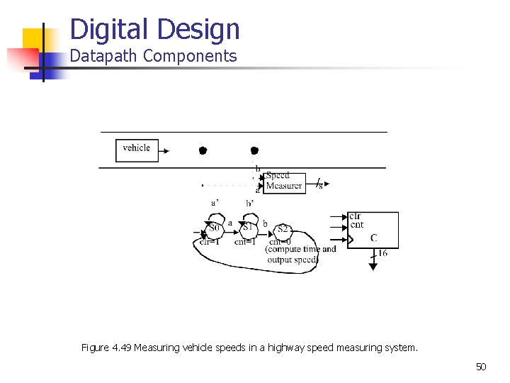
Digital Design Datapath Components Figure 4. 49 Measuring vehicle speeds in a highway speed measuring system. 50

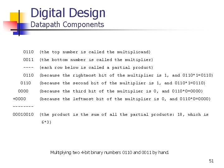
Digital Design Datapath Components 0110 (the top number is called the multiplicand) 0011 (the bottom number is called the multiplier) ---- (each row below is called a partial product) 0110 (because the rightmost bit of the multiplier is 1, and 0110*1=0110) 0110 0000 +0000 (because the second bit of the multiplier is 1, and 0110*1=0110) (because third bit of the multiplier is 0, and 0110*0=0000) (because the leftmost bit of the multiplier is 0, and 0110*0=0000) -------00010010 (the product is the sum of all the partial products: 18, which is 6*3) Multiplying two 4 -bit binary numbers 0110 and 0011 by hand. 51

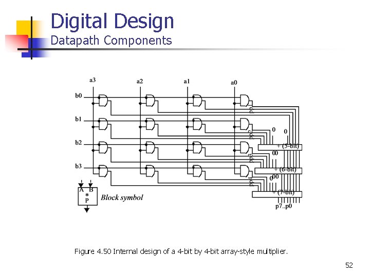
Digital Design Datapath Components Figure 4. 50 Internal design of a 4 -bit by 4 -bit array-style multiplier. 52

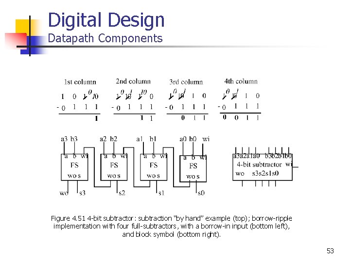
Digital Design Datapath Components Figure 4. 51 4 -bit subtractor: subtraction “by hand” example (top); borrow-ripple implementation with four full-subtractors, with a borrow-in input (bottom left), and block symbol (bottom right). 53

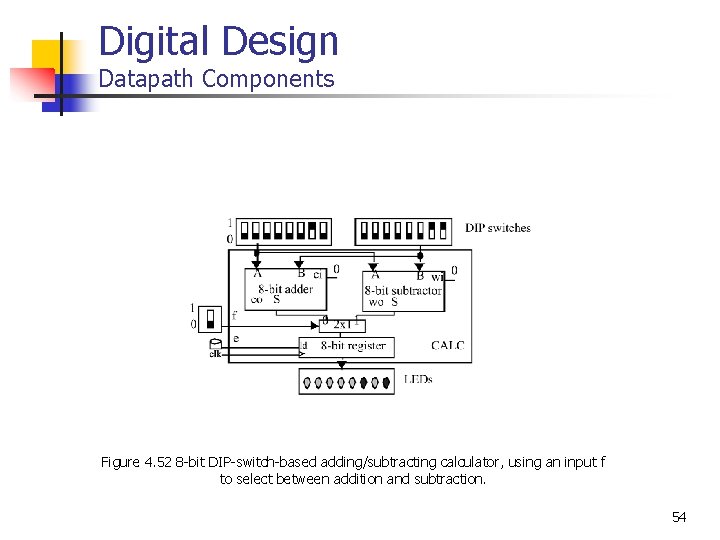
Digital Design Datapath Components Figure 4. 52 8 -bit DIP-switch-based adding/subtracting calculator, using an input f to select between addition and subtraction. 54

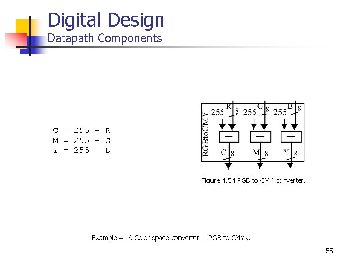
Digital Design Datapath Components C = 255 - R M = 255 - G Y = 255 - B Figure 4. 54 RGB to CMY converter. Example 4. 19 Color space converter -- RGB to CMYK. 55

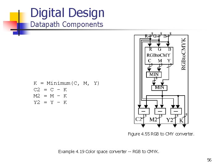
Digital Design Datapath Components K = Minimum(C, M, Y) C 2 = C - K M 2 = M - K Y 2 = Y - K Figure 4. 55 RGB to CMY converter. Example 4. 19 Color space converter -- RGB to CMYK. 56

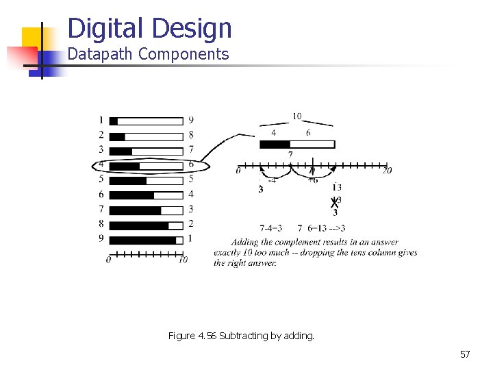
Digital Design Datapath Components Figure 4. 56 Subtracting by adding. 57

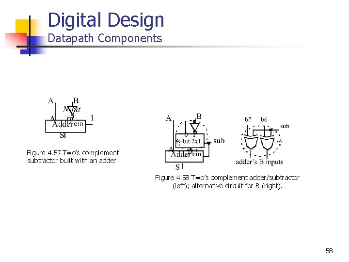
Digital Design Datapath Components Figure 4. 57 Two’s complement subtractor built with an adder. Figure 4. 58 Two’s complement adder/subtractor (left); alternative circuit for B (right). 58

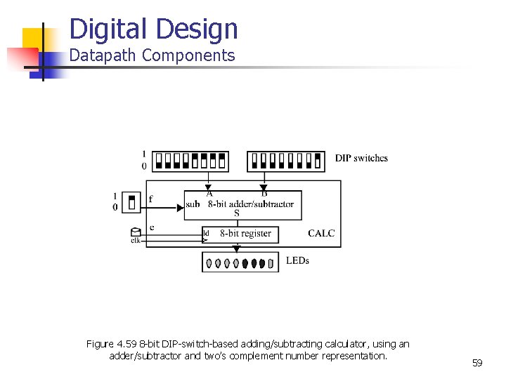
Digital Design Datapath Components Figure 4. 59 8 -bit DIP-switch-based adding/subtracting calculator, using an adder/subtractor and two’s complement number representation. 59

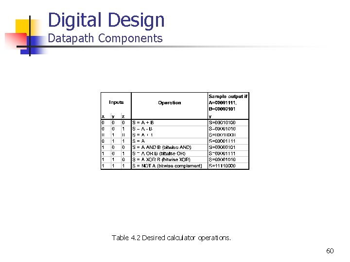
Digital Design Datapath Components Table 4. 2 Desired calculator operations. 60

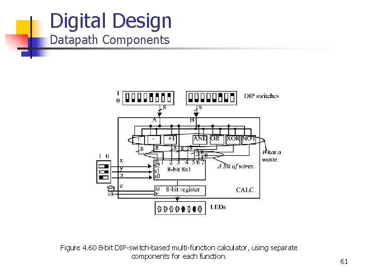
Digital Design Datapath Components Figure 4. 60 8 -bit DIP-switch-based multi-function calculator, using separate components for each function. 61

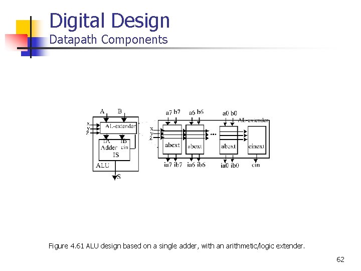
Digital Design Datapath Components Figure 4. 61 ALU design based on a single adder, with an arithmetic/logic extender. 62

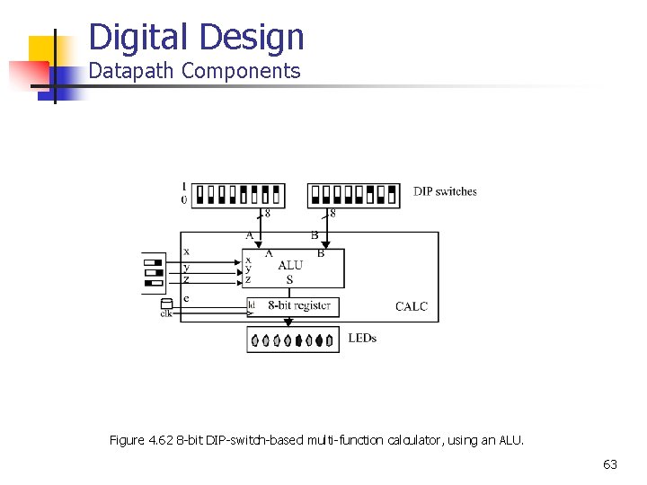
Digital Design Datapath Components Figure 4. 62 8 -bit DIP-switch-based multi-function calculator, using an ALU. 63

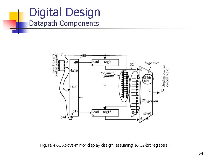
Digital Design Datapath Components Figure 4. 63 Above-mirror display design, assuming 16 32 -bit registers. 64

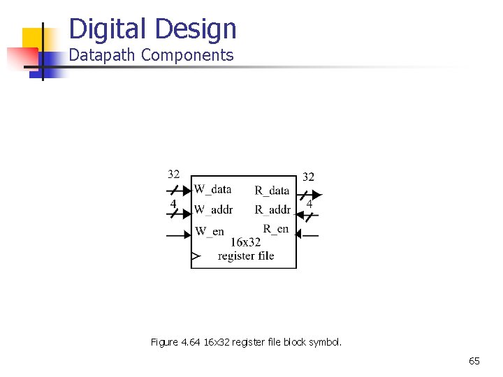
Digital Design Datapath Components Figure 4. 64 16 x 32 register file block symbol. 65

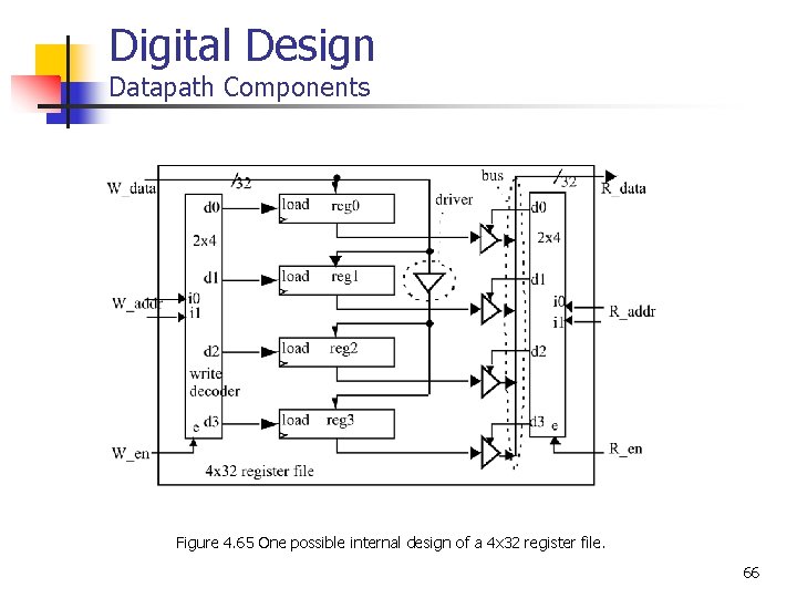
Digital Design Datapath Components Figure 4. 65 One possible internal design of a 4 x 32 register file. 66

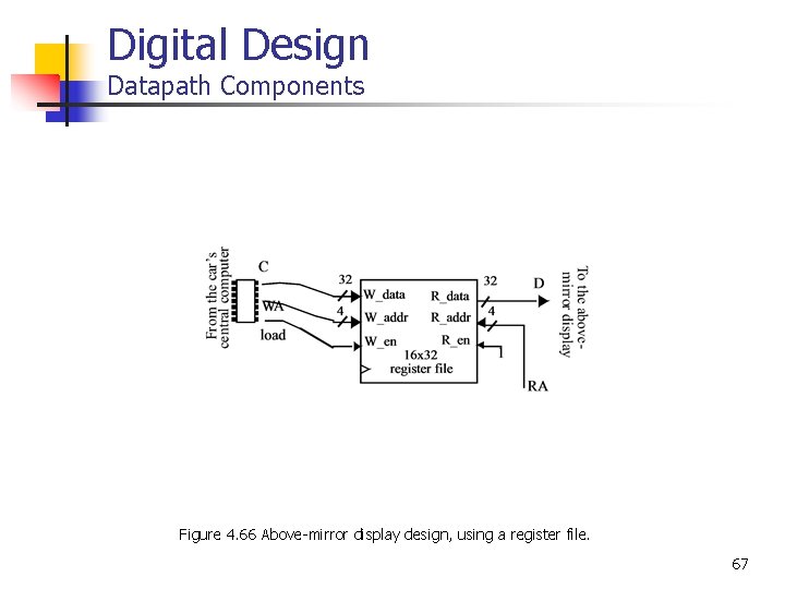
Digital Design Datapath Components Figure 4. 66 Above-mirror display design, using a register file. 67

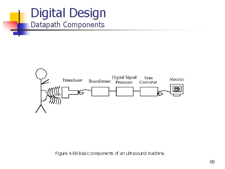
Digital Design Datapath Components Figure 4. 68 Basic components of an ultrasound machine. 68

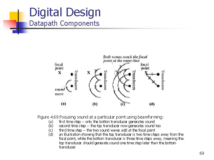
Digital Design Datapath Components Figure 4. 69 Focusing sound at a particular point using beamforming: (a) (b) (c) (d) first time step -- only the botton transducer generates sound second time step -- the top transducer now generates sound too third time step -- the two sound waves add at the focal point an illustration showing that the top transducer is two time steps away from the focal point, while the bottom transducer is three time steps away, meaning the top transducer should generate sound one time step later than the bottom transducer 69

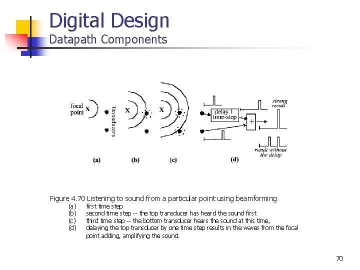
Digital Design Datapath Components Figure 4. 70 Listening to sound from a particular point using beamforming (a) (b) (c) (d) first time step second time step -- the top transducer has heard the sound first third time step -- the bottom transducer hears the sound at this time, delaying the top transducer by one time step results in the waves from the focal point adding, amplifying the sound. 70

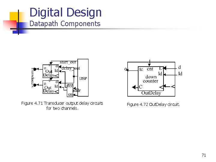
Digital Design Datapath Components Figure 4. 71 Transducer output delay circuits for two channels. Figure 4. 72 Out. Delay circuit. 71

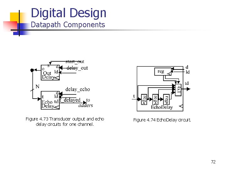
Digital Design Datapath Components Figure 4. 73 Transducer output and echo delay circuits for one channel. Figure 4. 74 Echo. Delay circuit. 72

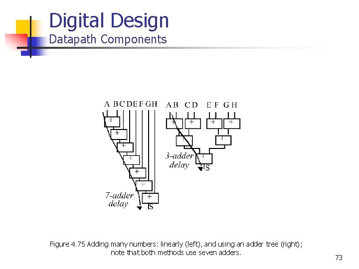
Digital Design Datapath Components Figure 4. 75 Adding many numbers: linearly (left), and using an adder tree (right); note that both methods use seven adders. 73

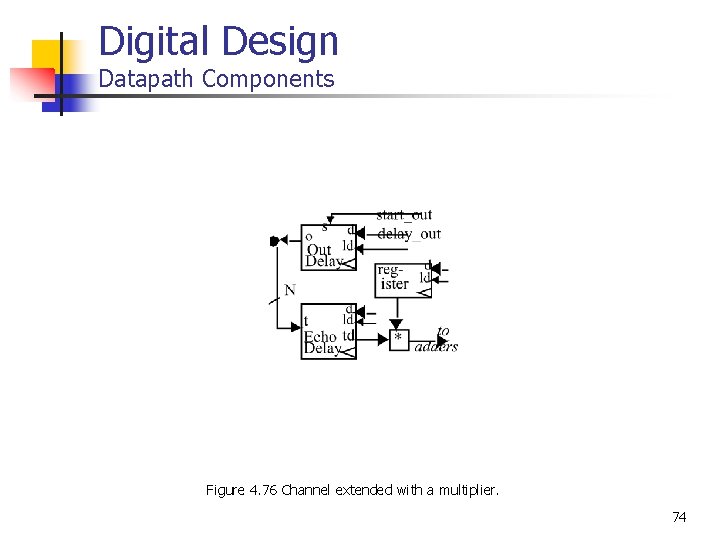
Digital Design Datapath Components Figure 4. 76 Channel extended with a multiplier. 74