Digital Design Computer Arch Lecture 3 b Introduction
Digital Design & Computer Arch. Lecture 3 b: Introduction to the Labs and FPGAs Prof. Onur Mutlu (Lecture by Hasan Hassan) ETH Zurich Spring 2020 27 February 2020 1
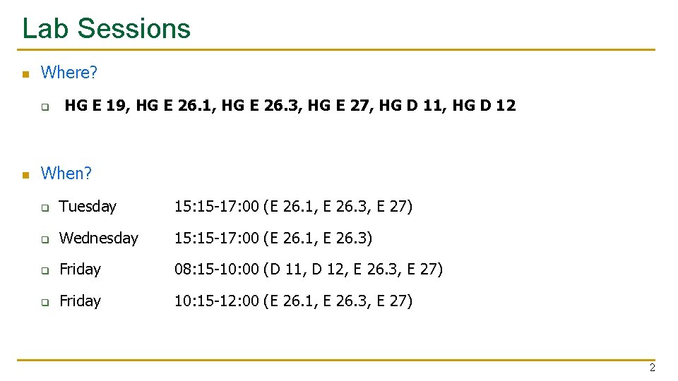
Lab Sessions n Where? q n HG E 19, HG E 26. 1, HG E 26. 3, HG E 27, HG D 11, HG D 12 When? q Tuesday 15: 15 -17: 00 (E 26. 1, E 26. 3, E 27) q Wednesday 15: 15 -17: 00 (E 26. 1, E 26. 3) q Friday 08: 15 -10: 00 (D 11, D 12, E 26. 3, E 27) q Friday 10: 15 -12: 00 (E 26. 1, E 26. 3, E 27) 2
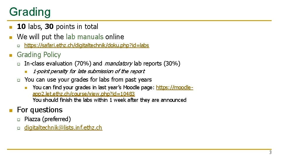
Grading n n 10 labs, 30 points in total We will put the lab manuals online q n https: //safari. ethz. ch/digitaltechnik/doku. php? id=labs Grading Policy q q In-class evaluation (70%) and mandatory lab reports (30%) n 1 -point penalty for late submission of the report You can use your grades for labs from past years n n You can find your grades in last year’s Moodle page: https: //moodleapp 2. let. ethz. ch/course/view. php? id=10483 You should finish the labs within 1 week after they are announced For questions q q Piazza (preferred) digitaltechnik@lists. inf. ethz. ch 3
Agenda n Logistics n What We Will learn? n FPGAs in Today’s Systems n Overview of the Lab Exercises n What is an FPGA? n Programming an FPGA n Tutorial and Demo 4
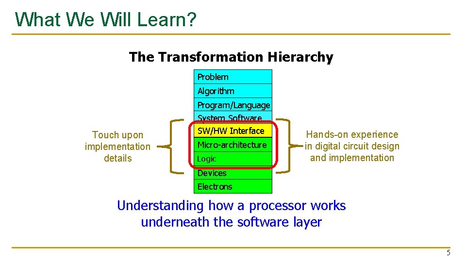
What We Will Learn? The Transformation Hierarchy Problem Algorithm Touch upon implementation details Program/Language System Software SW/HW Interface Micro-architecture Logic Hands-on experience in digital circuit design and implementation Devices Electrons Understanding how a processor works underneath the software layer 5
What We Will Learn? (2) n Considering the trade-offs between performance and area/complexity in your hardware implementation n Hands-on experience on: q Hardware Prototyping on FPGA q Debugging Your Hardware Implementation q Hardware Description Language (HDL) q Hardware Design Flow q Computer-Aided Design (CAD) Tools 6
Agenda n Logistics n What We Will learn? n FPGAs in Today’s Systems n Overview of the Lab Exercises n What is an FPGA? n Programming an FPGA n Tutorial and Demo 7
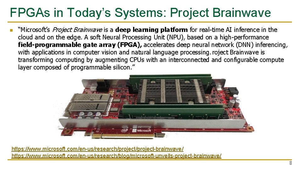
FPGAs in Today’s Systems: Project Brainwave n “Microsoft’s Project Brainwave is a deep learning platform for real-time AI inference in the cloud and on the edge. A soft Neural Processing Unit (NPU), based on a high-performance field-programmable gate array (FPGA), accelerates deep neural network (DNN) inferencing, with applications in computer vision and natural language processing. roject Brainwave is transforming computing by augmenting CPUs with an interconnected and configurable compute layer composed of programmable silicon. ” https: //www. microsoft. com/en-us/research/project-brainwave/ https: //www. microsoft. com/en-us/research/blog/microsoft-unveils-project-brainwave/ 8
FPGAs in Today’s Systems: Amazon EC 2 F 1 n “Amazon EC 2 F 1 instances use FPGAs to enable delivery of custom hardware accelerations. F 1 instances are easy to program and come with everything you need to develop, simulate, debug, and compile your hardware acceleration code, including an FPGA Developer AMI and supporting hardware level development on the cloud. Using F 1 instances to deploy hardware accelerations can be useful in many applications to solve complex science, engineering, and business problems that require high bandwidth, enhanced networking, and very high compute capabilities. ” https: //aws. amazon. com/ec 2/instance-types/f 1/ 9
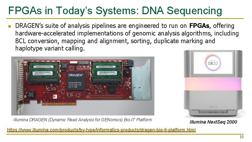
FPGAs in Today’s Systems: DNA Sequencing n DRAGEN’s suite of analysis pipelines are engineered to run on FPGAs, offering hardware-accelerated implementations of genomic analysis algorithms, including BCL conversion, mapping and alignment, sorting, duplicate marking and haplotype variant calling. Illumina DRAGEN (Dynamic Read Analysis for GENomics) Bio-IT Platform Illumina Next. Seq 2000 https: //www. illumina. com/products/by-type/informatics-products/dragen-bio-it-platform. html 10
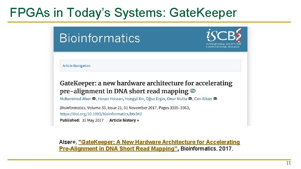
FPGAs in Today’s Systems: Gate. Keeper Alser+, "Gate. Keeper: A New Hardware Architecture for Accelerating Pre-Alignment in DNA Short Read Mapping”, Bioinformatics, 2017. 11
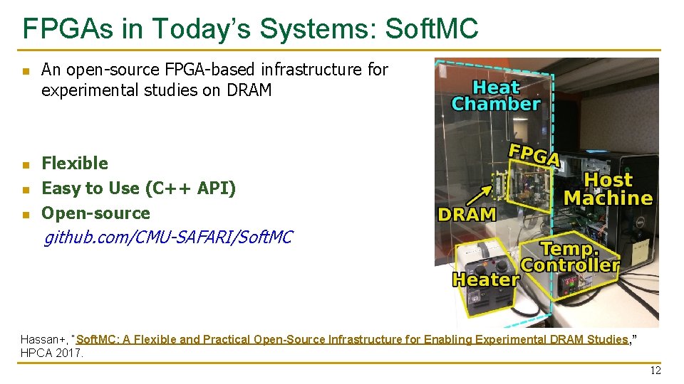
FPGAs in Today’s Systems: Soft. MC n n An open-source FPGA-based infrastructure for experimental studies on DRAM Flexible Easy to Use (C++ API) Open-source github. com/CMU-SAFARI/Soft. MC Hassan+, “Soft. MC: A Flexible and Practical Open-Source Infrastructure for Enabling Experimental DRAM Studies, ” HPCA 2017. 12
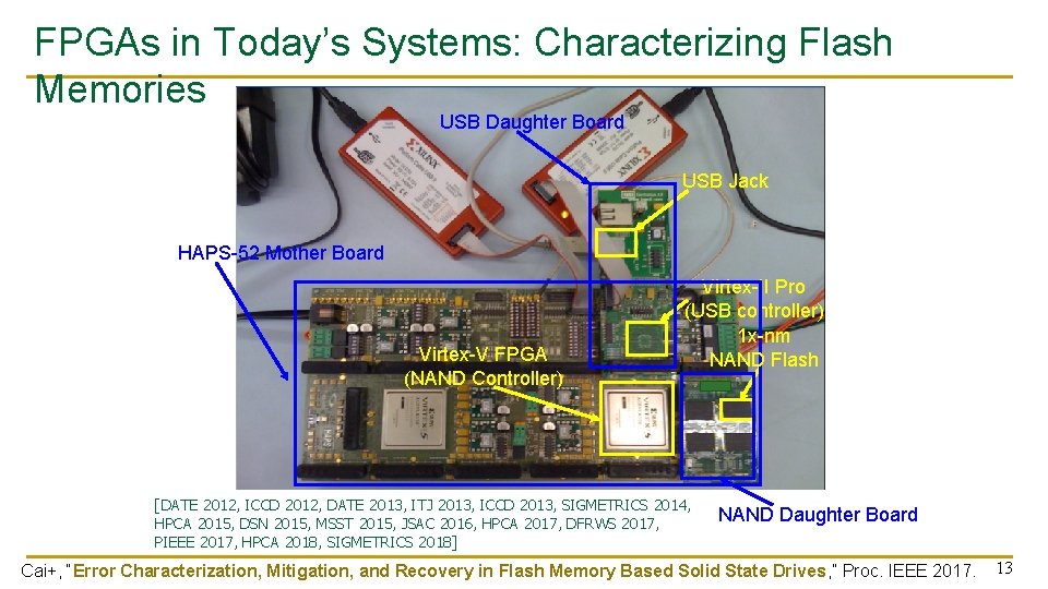
FPGAs in Today’s Systems: Characterizing Flash Memories USB Daughter Board USB Jack HAPS-52 Mother Board Virtex-V FPGA (NAND Controller) Virtex-II Pro (USB controller) 1 x-nm NAND Flash [DATE 2012, ICCD 2012, DATE 2013, ITJ 2013, ICCD 2013, SIGMETRICS 2014, HPCA 2015, DSN 2015, MSST 2015, JSAC 2016, HPCA 2017, DFRWS 2017, PIEEE 2017, HPCA 2018, SIGMETRICS 2018] NAND Daughter Board Cai+, “Error Characterization, Mitigation, and Recovery in Flash Memory Based Solid State Drives, ” Proc. IEEE 2017. 13
Agenda n Logistics n What We Will learn? n FPGAs in Today’s Systems n Overview of the Lab Exercises n What is an FPGA? n Programming an FPGA n Tutorial and Demo 14
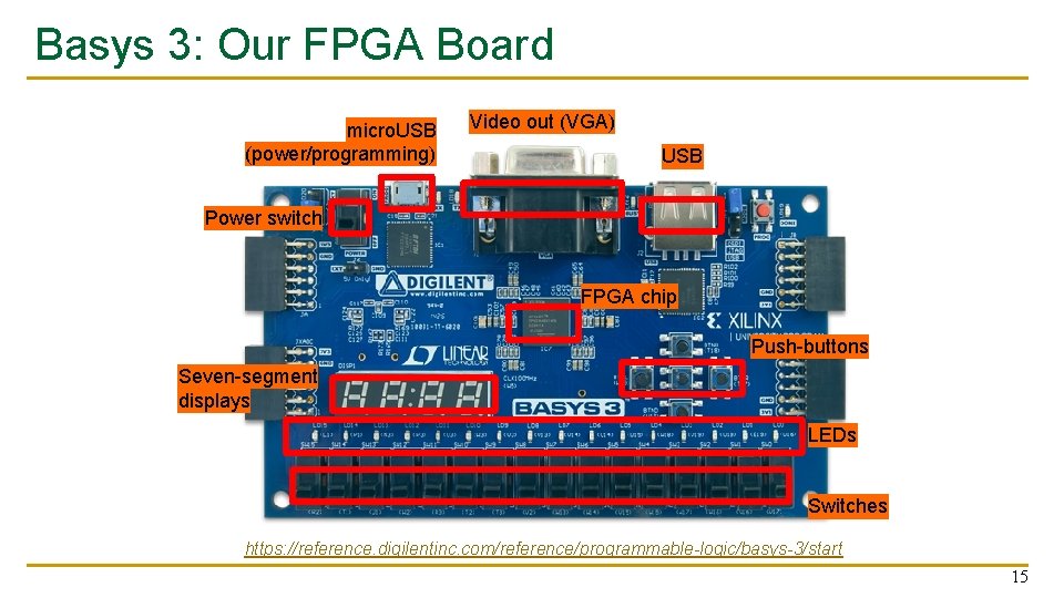
Basys 3: Our FPGA Board micro. USB (power/programming) Video out (VGA) USB Power switch FPGA chip Push-buttons Seven-segment displays LEDs Switches https: //reference. digilentinc. com/reference/programmable-logic/basys-3/start 15
High Level Labs Summary n At the end of the exercises, we will have built a 32 -bit microprocessor running on the FPGA board q n Each week we will have a new exercise q n It will be a small processor, but it will be able to execute pretty much any program Not all exercises will require the FPGA board You are encouraged to experiment with the board on your own q q We may have some extra boards for those who are interested It is not possible to destroy the board by programming! 16
Lab 1: Drawing a Basic Circuit n Comparison is a common operation in software programming q n n We usually want to know the relation between two variables (e. g. , <, >, ==, …) We will compare two electrical signals (inputs), and find whether they are same q The result (output) is also an electrical signal No FPGA programming involved q We encourage you to try later 17
Lab 2: Mapping Your Circuit to FPGA n Another common operation in software programming? q Addition n Design a circuit that adds two 1 -bit numbers n Reuse the 1 -bit adder multiple times to perform 4 -bit addition n Implement the design on the FPGA board q q Input: switches Output: LEDs 18
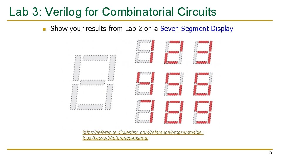
Lab 3: Verilog for Combinatorial Circuits n Show your results from Lab 2 on a Seven Segment Display https: //reference. digilentinc. com/reference/programmablelogic/basys-3/reference-manual 19
Lab 4: Finite State Machines n Blinking LEDs for a car’s turn signals q Implement and use memories q Change the blinking speed 20
Lab 5: Implementing an ALU n Towards implementing your very first processor n Implement your own Arithmetic and Logic Unit (ALU) n An ALU is an important part of the CPU q q Arithmetic operations: add, subtract, multiply, compare, … Logic operations: AND, OR, … 21
Lab 6: Testing the ALU n Simulate your design from Lab 5 n Learn how to debug your implementation to resolve problems 22
Lab 7: Writing Assembly Code n Programming in assembly language q MIPS n Implement a program which you will later use to run on your processor n Image manipulation 23
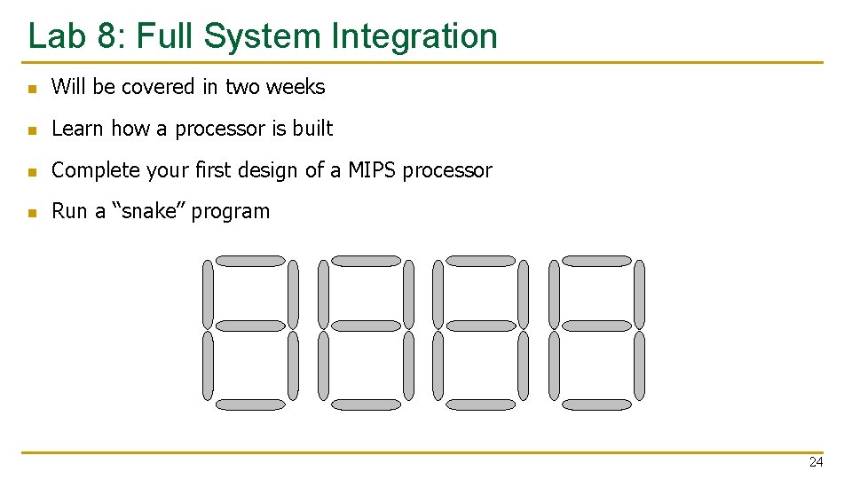
Lab 8: Full System Integration n Will be covered in two weeks n Learn how a processor is built n Complete your first design of a MIPS processor n Run a “snake” program 24
Lab 9: The Performance of MIPS n Improve the performance of your processor from Lab 8 by adding new instructions q Multiplication q Bit shifting 25
Agenda n Logistics n What We Will learn? n FPGAs in Today’s Systems n Overview of the Lab Exercises n What is an FPGA? n Programming an FPGA n Tutorial and Demo 26

Basys 3: Our FPGA Board micro. USB (power/programming) Video out (VGA) USB Power switch FPGA chip Push-buttons Seven-segment displays LEDs Switches https: //reference. digilentinc. com/reference/programmable-logic/basys-3/start 27
What is an FPGA? n Field Programmable Gate Array n FPGA is a reconfigurable substrate q q n Reconfigurable functions Reconfigurable interconnection of functions Reconfigurable input/output (IO) … FPGAs fill the gap between software and hardware q q Achieves higher performance than software Maintains more flexibility than hardware 28
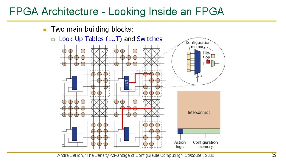
FPGA Architecture - Looking Inside an FPGA n Two main building blocks: q Look-Up Tables (LUT) and Switches Andre De. Hon, “The Density Advantage of Configurable Computing”, Computer, 2000 29
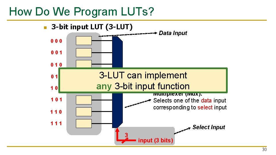
How Do We Program LUTs? n 3 -bit input LUT (3 -LUT) Data Input 000 001 010 011 100 3 -LUT can implement output (1 bit) any 3 -bit input function Multiplexer (Mux): Selects one of the data input corresponding to select input 101 110 111 Select Input 3 input (3 bits) 30
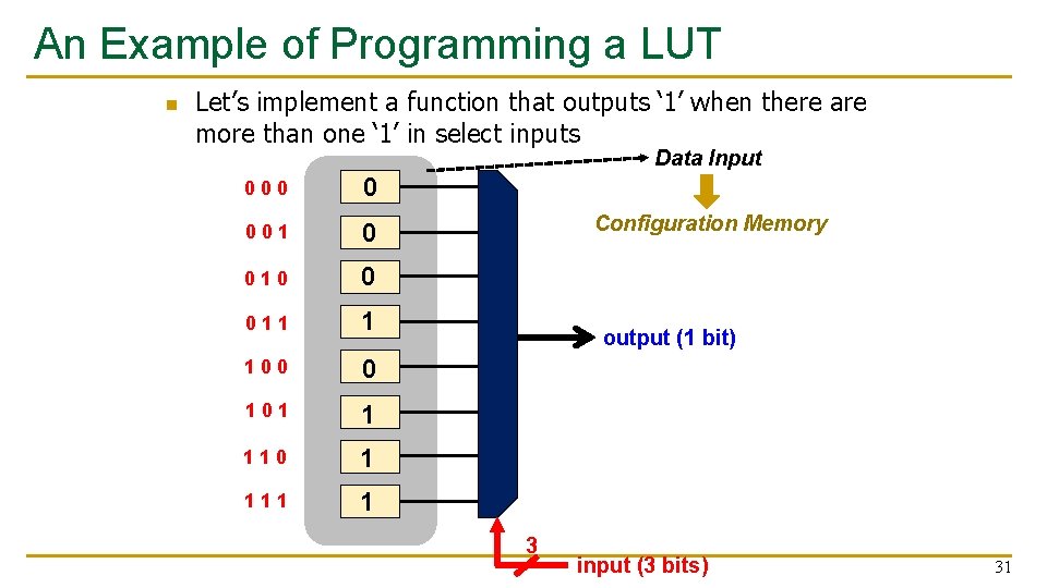
An Example of Programming a LUT n Let’s implement a function that outputs ‘ 1’ when there are more than one ‘ 1’ in select inputs Data Input 000 0 001 0 010 0 011 1 100 0 101 1 110 1 111 1 Configuration Memory output (1 bit) 3 input (3 bits) 31
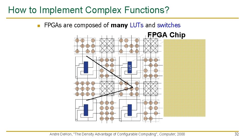
How to Implement Complex Functions? n FPGAs are composed of many LUTs and switches FPGA Chip Andre De. Hon, “The Density Advantage of Configurable Computing”, Computer, 2000 32
Modern FPGA Architectures n Typically 6 -LUTs q Thousands of them n MBs of distributed on-chip memory n Hard-coded special-purpose hardware blocks for high-performance operations q q q n Memory interface Low latency and high bandwidth off-chip I/O … Even a processor embedded within the FPGA chip 33
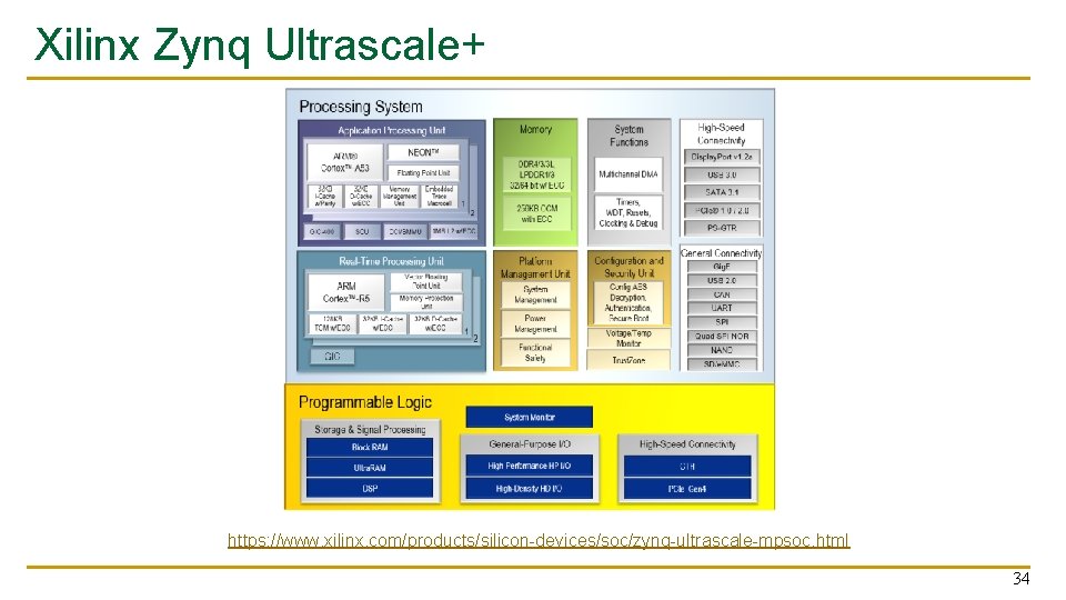
Xilinx Zynq Ultrascale+ https: //www. xilinx. com/products/silicon-devices/soc/zynq-ultrascale-mpsoc. html 34
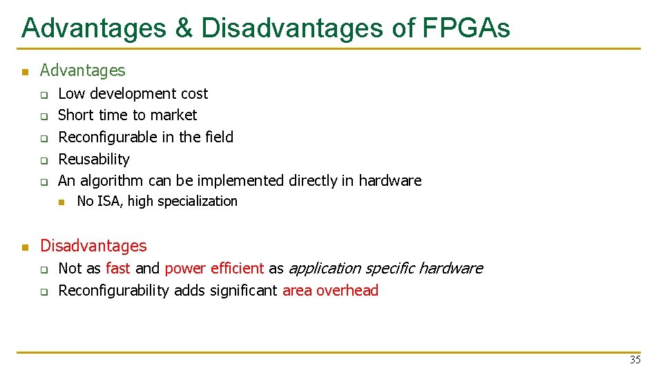
Advantages & Disadvantages of FPGAs n Advantages q q q Low development cost Short time to market Reconfigurable in the field Reusability An algorithm can be implemented directly in hardware n n No ISA, high specialization Disadvantages q q Not as fast and power efficient as application specific hardware Reconfigurability adds significant area overhead 35
Agenda n Logistics n What We Will learn? n FPGAs in Today’s Systems n Overview of the Lab Exercises n What is an FPGA? n Programming an FPGA n Tutorial and Demo 36
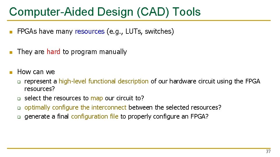
Computer-Aided Design (CAD) Tools n FPGAs have many resources (e. g. , LUTs, switches) n They are hard to program manually n How can we q q represent a high-level functional description of our hardware circuit using the FPGA resources? select the resources to map our circuit to? optimally configure the interconnect between the selected resources? generate a final configuration file to properly configure an FPGA? 37
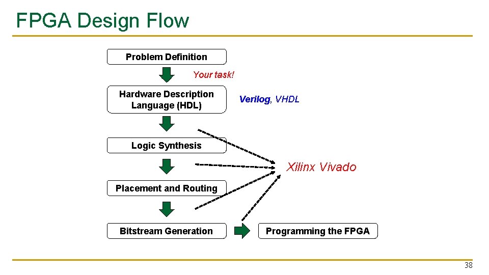
FPGA Design Flow Problem Definition Your task! Hardware Description Language (HDL) Verilog, VHDL Logic Synthesis Xilinx Vivado Placement and Routing Bitstream Generation Programming the FPGA 38
Vivado n IDE-like software that helps us throughout the FPGA design flow n Provides tools to simulate our designs q q n n Validate the correctness of the implementation Debugging Provides drivers and graphical interface to easily program the FPGA using a USB cable Installed in computer rooms in HG (E 19, E 26. 1, E 26. 3, E 27) 39
Tutorial and Demo n We will see how to q q q n use Vivado to write Verilog code follow the FPGA design flow steps download the bitstream into the FPGA Simple Keyboard Demo q An example for a simple hardware that you can easily develop by the end of semester https: //reference. digilentinc. com/learn/programmable-logic/tutorials/basys-3 -keyboard-demo/start 40
Today We Covered: n Logistics n What We Will learn? n FPGAs in Today’s Systems n Overview of the Lab Exercises n What is an FPGA? n Programming an FPGA n Tutorial and Demo 41
Digital Design & Computer Arch. Lecture 3 b: Introduction to the Labs and FPGAs Prof. Onur Mutlu (Lecture by Hasan Hassan) ETH Zurich Spring 2020 27 February 2020 42
- Slides: 42