Digital Design Computer Arch Lab 5 Supplement Implementing

Digital Design & Computer Arch. Lab 5 Supplement: Implementing an ALU Prof. Onur Mutlu ETH Zürich Spring 2020 27 March 2020
What Will We Learn? n n In lab 5, you will Implement an Arithmetic Logic Unit (ALU) in Verilog and evaluate its speed and resource utilization. Draw a block level diagram of the MIPS 32 -bit ALU, based on the description in the textbook. Implement the ALU using Verilog. Synthesize the ALU and evaluate speed and FPGA resource utilization. 2
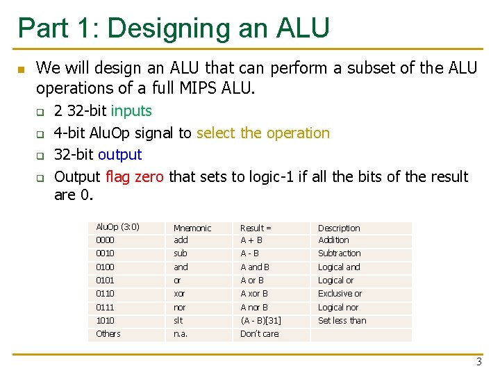
Part 1: Designing an ALU n We will design an ALU that can perform a subset of the ALU operations of a full MIPS ALU. q q 2 32 -bit inputs 4 -bit Alu. Op signal to select the operation 32 -bit output Output flag zero that sets to logic-1 if all the bits of the result are 0. Alu. Op (3: 0) 0000 Mnemonic add Result = A+B Description Addition 0010 sub A-B Subtraction 0100 and A and B Logical and 0101 or A or B Logical or 0110 xor A xor B Exclusive or 0111 nor A nor B Logical nor 1010 slt (A - B)[31] Set less than Others n. a. Don’t care 3
Part 1: Designing an ALU- Block Diagram n First, you need to draw a block diagram of the ALU, like the n one seen in Figure 5. 15 of the H&H textbook. You are free to chose if you want to draw the complete block diagram or split it up into modules and elaborate the modules, similar to the next slide. 4
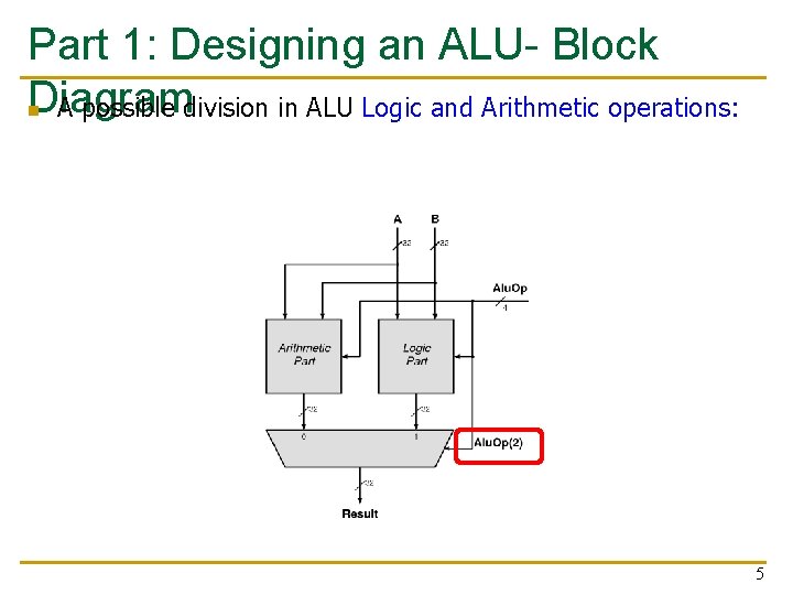
Part 1: Designing an ALU- Block Diagram n A possible division in ALU Logic and Arithmetic operations: 5
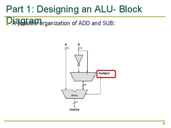
Part 1: Designing an ALU- Block Diagram n A possible organization of ADD and SUB: 6
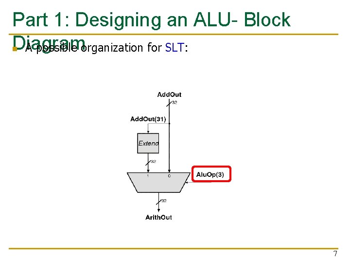
Part 1: Designing an ALU- Block Diagram n A possible organization for SLT: 7
Part 2: Implementation n Replace each block with a Verilog description. n Synthesize and implement your design. n We do not transfer the design to FPGA in this lab q n No Constraint file Bitstream generation will fail. At this point, we cannot verify the correctness of our circuit manually. q q You will calculate how long will the exhaustive search take. You learn how to use testbench to test the correctness of this circuit in lab 6! 8
Part 3: The performance of the circuit (I) n In this lab, we will learn to check: q q n The speed (i. e. , max frequency our circuit can run at) The area (i. e. , FPGA resource utilization). We will add a timing constraint to set the maximum delay that we would like our ALU to have. 9
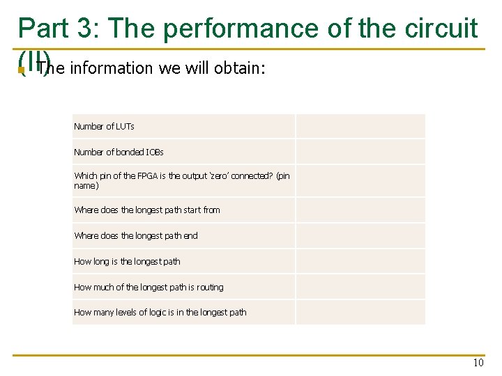
Part 3: The performance of the circuit (II) n The information we will obtain: Number of LUTs Number of bonded IOBs Which pin of the FPGA is the output ‘zero’ connected? (pin name) Where does the longest path start from Where does the longest path end How long is the longest path How much of the longest path is routing How many levels of logic is in the longest path 10
Last Words n n n In lab 5, you will Implement an Arithmetic Logic Unit (ALU) in Verilog and evaluate its speed and resource utilization. Draw a block level diagram of the MIPS 32 -bit ALU, based on the description in the textbook. Implement the ALU using Verilog. Synthesize the ALU and evaluate speed and FPGA resource utilization. In the report, you will use your adder from Lab 2 in the ALU and compare the resource utilization. 11
Report Deadline 23: 59, 24 April 2020 12

Digital Design & Computer Arch. Lab 5 Supplement: Implementing an ALU Prof. Onur Mutlu ETH Zürich Spring 2020 27 March 2020
- Slides: 13