Digital Design Chapter 7 Physical Implementation Slides to
- Slides: 40

Digital Design Chapter 7: Physical Implementation Slides to accompany the textbook Digital Design, First Edition, by Frank Vahid, John Wiley and Sons Publishers, 2007. http: //www. ddvahid. com Copyright © 2007 Frank Vahid Instructors of courses requiring Vahid's Digital Design textbook (published by John Wiley and Sons) have permission to modify and use these slides for customary course-related activities, subject to keeping this copyright notice in place and unmodified. These slides may be posted as unanimated pdf versions on publicly-accessible course websites. . Power. Point source (or pdf Digital Design with animations) may not be posted to publicly-accessible websites, but may be posted for students on internal protected sites or distributed directly to students by other electronic means. Copyright © 2006 1 Instructors may make printouts of the slides available to students for a reasonable photocopying charge, without incurring royalties. Any other use requires explicit permission. Instructors Franksource Vahid may obtain Power. Point or obtain special use permissions from Wiley – see http: //www. ddvahid. com for information.

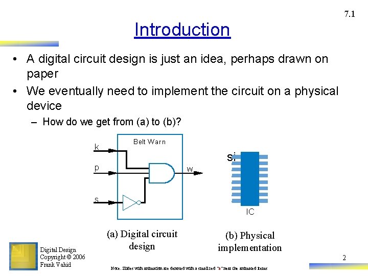
7. 1 Introduction • A digital circuit design is just an idea, perhaps drawn on paper • We eventually need to implement the circuit on a physical device – How do we get from (a) to (b)? k Belt W arn si p w s IC Digital Design Copyright © 2006 Frank Vahid (a) Digital circuit design (b) Physical implementation 2 Note: Slides with animation are denoted with a small red "a" near the animated items

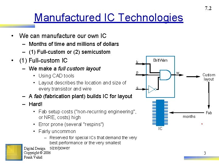
7. 2 Manufactured IC Technologies • We can manufacture our own IC – Months of time and millions of dollars – (1) Full-custom or (2) semicustom • (1) Full-custom IC – We make a full custom layout • Using CAD tools • Layout describes the location and size of every transistor and wire k Belt. Warn p w Custom layout s – A fab (fabrication plant) builds IC for layout – Hard! • Fab setup costs ("non-recurring engineering", or NRE, costs) high • Error prone (several "respins") • Fairly uncommon Fab months a IC – Reserved for special ICs that demand the very best performance or the very smallest Digital Design size/power Copyright © 2006 Frank Vahid 3

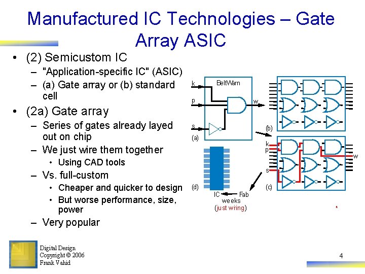
Manufactured IC Technologies – Gate Array ASIC • (2) Semicustom IC – "Application-specific IC" (ASIC) – (a) Gate array or (b) standard cell • (2 a) Gate array – Series of gates already layed out on chip – We just wire them together k Belt. Warn p w s (b) (a) k p • Using CAD tools s – Vs. full-custom • Cheaper and quicker to design • But worse performance, size, power w (d) (c) IC Fab weeks (just wiring) a – Very popular Digital Design Copyright © 2006 Frank Vahid 4

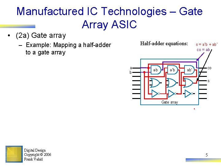
Manufactured IC Technologies – Gate Array ASIC • (2 a) Gate array Half-adder equations: – Example: Mapping a half-adder to a gate array a b ab a'b s = a'b + ab' co = ab co ab' s Gate array a Digital Design Copyright © 2006 Frank Vahid 5

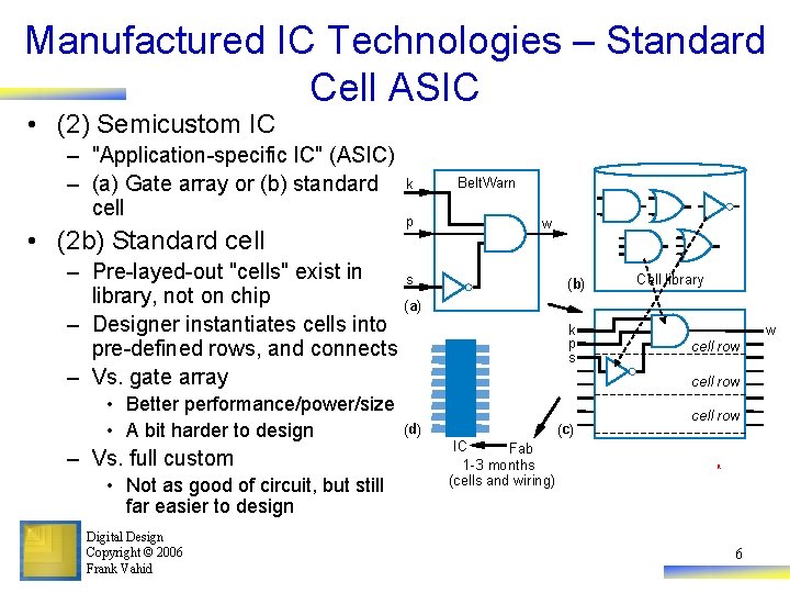
Manufactured IC Technologies – Standard Cell ASIC • (2) Semicustom IC – "Application-specific IC" (ASIC) – (a) Gate array or (b) standard cell • (2 b) Standard cell k p Belt. Warn w – Pre-layed-out "cells" exist in s library, not on chip (a) – Designer instantiates cells into pre-defined rows, and connects – Vs. gate array • Better performance/power/size • A bit harder to design – Vs. full custom • Not as good of circuit, but still far easier to design Digital Design Copyright © 2006 Frank Vahid (b) k p s Cell library w cell row (d) (c) IC Fab 1 -3 months (cells and wiring) cell row a 6

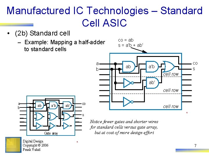
Manufactured IC Technologies – Standard Cell ASIC • (2 b) Standard cell – Example: Mapping a half-adder to standard cells a b co = ab s = a'b + ab' ab co s a'b cell row ab' cell row a b ab a'b co ab' cell row a s Notice fewer gates and shorter wires for standard cells versus gate array, but at cost of more design effort Gate array Digital Design Copyright © 2006 Frank Vahid a 7

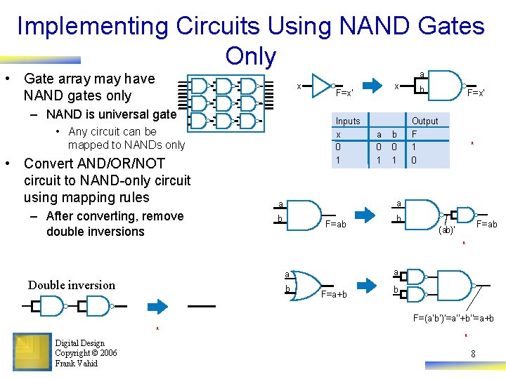
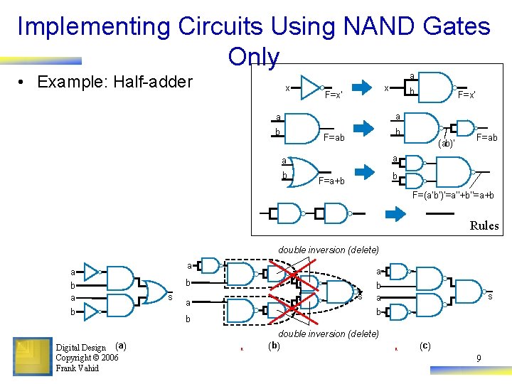
Implementing Circuits Using NAND Gates Only a • Gate array may have NAND gates only x – NAND is universal gate Inputs x 0 1 • Any circuit can be mapped to NANDs only • Convert AND/OR/NOT circuit to NAND-only circuit using mapping rules – After converting, remove double inversions x F=x' a 0 1 b F=x' Output F 1 0 a a a b F=ab (ab)' a a a Double inversion b F=a+b b F=(a'b')'=a''+b''=a+b a a Digital Design Copyright © 2006 Frank Vahid 8

Implementing Circuits Using NAND Gates Only a • Example: Half-adder x x F=x' b F=x' a a b b F=ab (ab)' a a b F=ab b F=a+b F=(a'b')'=a''+b''=a+b Rules double inversion (delete) a b Digital Design (a) Copyright © 2006 Frank Vahid a a b s s a b a s b b a double inversion (delete) (b) a (c) 9

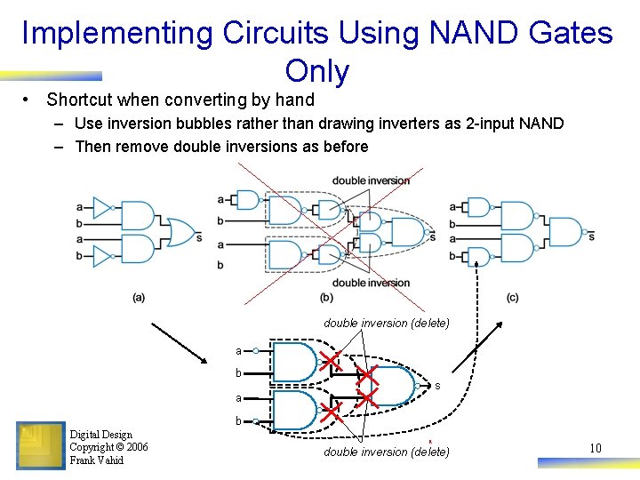
Implementing Circuits Using NAND Gates Only • Shortcut when converting by hand – Use inversion bubbles rather than drawing inverters as 2 -input NAND – Then remove double inversions as before double inversion (delete) a b s a b Digital Design Copyright © 2006 Frank Vahid a double inversion (delete) 10

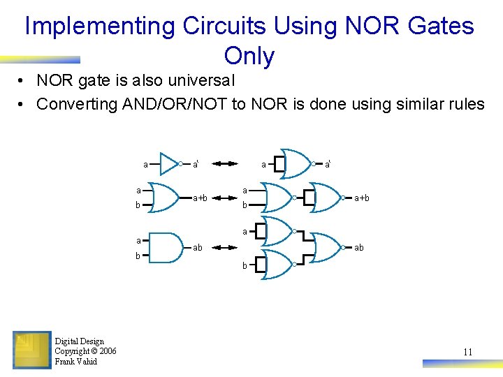
Implementing Circuits Using NOR Gates Only • NOR gate is also universal • Converting AND/OR/NOT to NOR is done using similar rules a a b Digital Design Copyright © 2006 Frank Vahid a‘ a+b a a b a‘ a+b a ab ab b 11

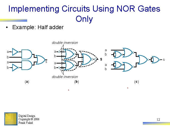
Implementing Circuits Using NOR Gates Only • Example: Half adder double inversion a b a b a s b (a) s a b double inversion (b) (c) a a Digital Design Copyright © 2006 Frank Vahid 12

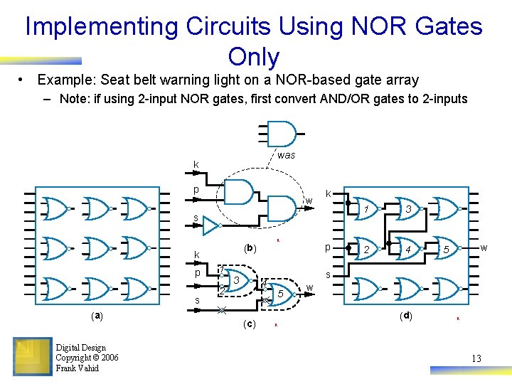
Implementing Circuits Using NOR Gates Only • Example: Seat belt warning light on a NOR-based gate array – Note: if using 2 -input NOR gates, first convert AND/OR gates to 2 -inputs was k p w k s k p s (a) Digital Design Copyright © 2006 Frank Vahid a (b) 1 3 4 2 (c) p 1 3 2 4 w 5 s 5 w (d) a a 13

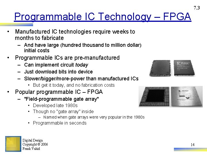
7. 3 Programmable IC Technology – FPGA • Manufactured IC technologies require weeks to months to fabricate – And have large (hundred thousand to million dollar) initial costs • Programmable ICs are pre-manufactured – Can implement circuit today – Just download bits into device – Slower/bigger/more-power than manufactured ICs • But get it today, and no fabrication costs • Popular programmable IC – FPGA – "Field-programmable gate array" • Developed late 1980 s • Though no "gate array" inside – Named when gate arrays were very popular in the 1980 s • Programmable in seconds Digital Design Copyright © 2006 Frank Vahid 14

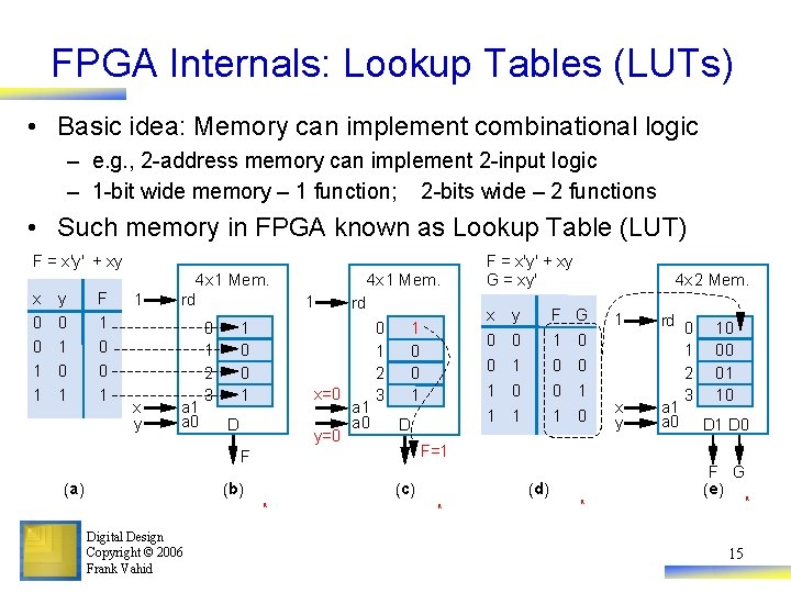
FPGA Internals: Lookup Tables (LUTs) • Basic idea: Memory can implement combinational logic – e. g. , 2 -address memory can implement 2 -input logic – 1 -bit wide memory – 1 function; 2 -bits wide – 2 functions • Such memory in FPGA known as Lookup Table (LUT) F = x'y' + xy 4 x 1 Mem. x 0 0 1 1 y 0 1 F 1 0 0 1 1 x y rd a 1 a 0 4 x 1 Mem. 1 0 1 2 3 1 0 0 1 x=0 D y=0 rd a 1 a 0 0 1 2 3 D a 4 x 2 Mem. y F G 0 0 1 1 1 1 0 1 x y rd 0 10 1 00 2 01 3 10 a 1 a 0 D 1 D 0 F=1 (c) (b) Digital Design Copyright © 2006 Frank Vahid x 1 0 0 1 F (a) F = x'y' + xy G = xy' (d ) a a F G (e) a 15

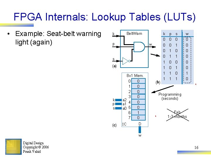
FPGA Internals: Lookup Tables (LUTs) • Example: Seat-belt warning light (again) k Belt. Warn p w s (a) k p s (c) 8 x 1 Mem. 0 0 1 0 2 0 3 0 a 2 0 a 1 4 0 a 0 5 6 1 7 0 IC (b) k 0 0 1 1 p 0 0 1 1 s 0 1 0 1 w 0 0 0 1 0 a Programming (seconds) a Fab 1 -3 months D w Digital Design Copyright © 2006 Frank Vahid 16

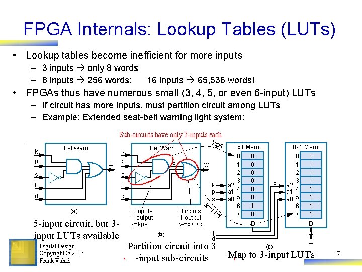
FPGA Internals: Lookup Tables (LUTs) • Lookup tables become inefficient for more inputs – 3 inputs only 8 words – 8 inputs 256 words; 16 inputs 65, 536 words! • FPGAs thus have numerous small (3, 4, 5, or even 6 -input) LUTs – If circuit has more inputs, must partition circuit among LUTs – Example: Extended seat-belt warning light system: Sub-circuits have only 3 -inputs each k Belt. Warn p k w p s s t t d d 5 -input circuit, but 3 input LUTs available Digital Design Copyright © 2006 Frank Vahid x 3 inputs 1 output x=kps' (a) w 3 inputs 1 output w=x+t+d (b) a kps' Belt. Warn x+ k p s t+ d 8 x 1 Mem. 0 1 2 3 a 2 a 1 4 a 0 5 6 7 0 0 0 1 0 x D D t d Partition circuit into 3 -input sub-circuits 8 x 1 Mem. 0 0 1 1 2 1 3 1 a 2 1 a 1 4 1 a 0 5 6 1 7 1 (c) w Map to 3 -input LUTs a 17

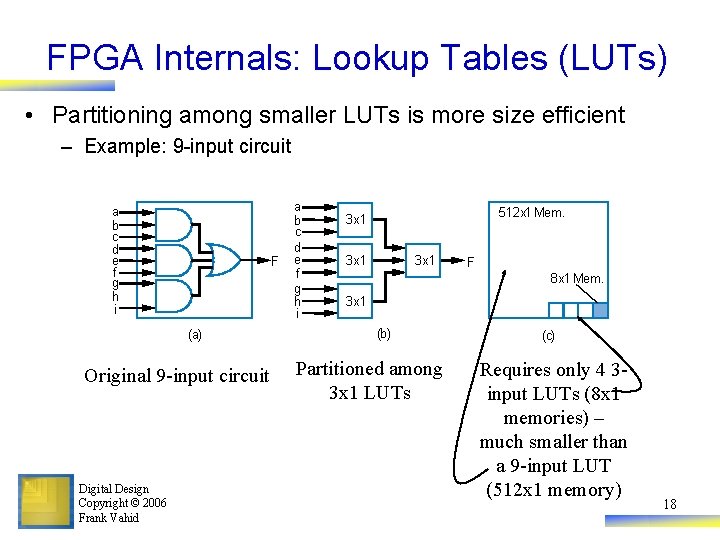
FPGA Internals: Lookup Tables (LUTs) • Partitioning among smaller LUTs is more size efficient – Example: 9 -input circuit a b c d e f g h i F (a) Original 9 -input circuit Digital Design Copyright © 2006 Frank Vahid a b c d e f g h i 512 x 1 Mem. 3 x 1 F 8 x 1 Mem. 3 x 1 (b) Partitioned among 3 x 1 LUTs (c) Requires only 4 3 input LUTs (8 x 1 memories) – much smaller than a 9 -input LUT (512 x 1 memory) 18

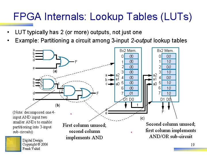
FPGA Internals: Lookup Tables (LUTs) • LUT typically has 2 (or more) outputs, not just one • Example: Partitioning a circuit among 3 -input 2 -output lookup tables a b c d 8 x 2 Mem. 0 F e a b c (a) 1 2 3 t d a b c 1 2 F 3 e 1 2 3 a 2 a 1 4 a 0 5 6 7 Digital Design Copyright © 2006 Frank Vahid 0 1 2 3 a 2 a 1 4 a 0 5 6 7 00 00 01 D 0 00 10 10 10 D 1 D 0 t (b) (Note: decomposed one 4 input AND input two smaller ANDs to enable partitioning into 3 -input sub-circuits) 8 x 2 Mem. a d e F (c) First column unused; second column implements AND a Second column unused; first column implements AND/OR sub-circuit 19

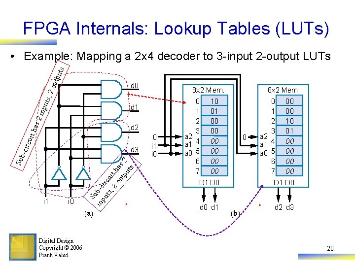
FPGA Internals: Lookup Tables (LUTs) out put s • Example: Mapping a 2 x 4 decoder to 3 -input 2 -output LUTs put s, 2 d 0 has 2 in d 1 -cir cuit d 2 i 1 i 0 Su in b-c pu ir ts, cui 2 o th ut as 2 pu ts Sub d 3 a (a) Digital Design Copyright © 2006 Frank Vahid 0 i 1 i 0 8 x 2 Mem. 0 10 1 01 2 00 3 00 a 2 a 1 4 00 a 0 5 00 6 00 7 00 0 8 x 2 Mem. 0 00 1 00 2 10 3 01 a 2 a 1 4 00 a 0 5 00 6 00 7 00 D 1 D 0 d 1 D 0 a (b) d 2 d 3 20

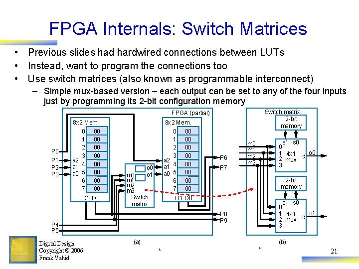
FPGA Internals: Switch Matrices • Previous slides had hardwired connections between LUTs • Instead, want to program the connections too • Use switch matrices (also known as programmable interconnect) – Simple mux-based version – each output can be set to any of the four inputs just by programming its 2 -bit configuration memory Switch matrix 2 -bit memory FPGA (partial) P 0 P 1 P 2 P 3 8 x 2 Mem. 0 00 1 00 2 00 3 00 a 2 a 1 4 00 a 0 5 00 6 00 7 00 D 1 D 0 8 x 2 Mem. 0 00 1 00 2 00 3 00 a 2 a 1 4 00 a 0 5 00 6 00 7 00 o 1 m 0 m 1 m 2 m 3 Switch matrix P 7 2 -bit memory D 1 D 0 s 1 s 0 i 0 o 1 i 1 4 x 1 i 2 mux d i 3 P 8 P 9 P 4 P 5 Digital Design Copyright © 2006 Frank Vahid P 6 s 1 s 0 i 0 o 0 i 1 4 x 1 i 2 mux d i 3 m 0 m 1 m 2 m 3 (a) (b) a a 21

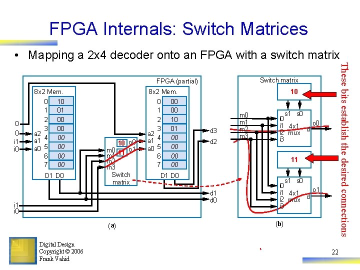
FPGA Internals: Switch Matrices • Mapping a 2 x 4 decoder onto an FPGA with a switch matrix 0 0 i 1 i 0 8 x 2 Mem. 0 1 2 3 a 2 a 1 4 a 0 5 6 7 10 01 00 00 00 D 1 D 0 10 o 0 m 0 11 o 1 m 2 m 3 Switch matrix 00 00 10 01 00 00 10 d 3 d 2 s 1 s 0 i 0 o 0 i 1 4 x 1 d i 2 mux i 3 m 0 m 1 m 2 m 3 11 D 0 s 1 s 0 i 0 o 1 i 1 4 x 1 d i 2 mux i 3 d 1 d 0 i 1 i 0 (b) (a) Digital Design Copyright © 2006 Frank Vahid These bits establish the desired connections Switch matrix FPGA (partial) a 22

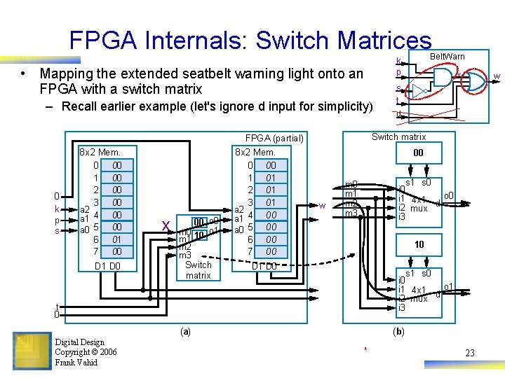
FPGA Internals: Switch Matrices • Mapping the extended seatbelt warning light onto an FPGA with a switch matrix 0 k p s D 1 D 0 x 00 o 0 m 0 10 o 1 m 2 m 3 Switch matrix t d 00 w s 1 s 0 i 0 o 0 i 1 4 x 1 d i 2 mux i 3 m 0 m 1 m 2 m 3 10 D 1 D 0 s 1 s 0 i 0 o 1 i 1 4 x 1 d i 2 mux i 3 t 0 (a) Digital Design Copyright © 2006 Frank Vahid w Switch matrix FPGA (partial) 8 x 2 Mem. 0 00 1 01 2 01 3 01 a 2 a 1 4 00 a 0 5 00 6 00 7 00 x s – Recall earlier example (let's ignore d input for simplicity) 8 x 2 Mem. 0 00 1 00 2 00 3 00 a 2 a 1 4 00 a 0 5 00 6 01 7 00 Belt. Warn k p (b) a 23

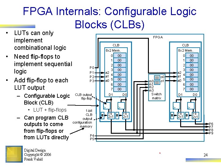
FPGA Internals: Configurable Logic Blocks (CLBs) • LUTs can only implement combinational logic • Need flip-flops to implement sequential logic • Add flip-flop to each LUT output – Configurable Logic Block (CLB) • LUT + flip-flops – Can program CLB outputs to come from flip-flops or from LUTs directly Digital Design Copyright © 2006 Frank Vahid FPGA CLB P 0 P 1 P 2 P 3 CLB output flip-flop 1 -bit CLB output configuration memory 8 x 2 Mem. 0 1 2 3 a 2 a 1 4 a 0 5 6 7 00 00 D 1 0 CLB 10 2 x 1 0 D 0 00 o 0 m 0 00 o 1 m 2 m 3 Switch matrix 10 D 1 0 2 x 1 10 2 x 1 0 00 00 D 0 10 2 x 1 P 6 P 7 P 8 P 9 P 4 P 5 a 24

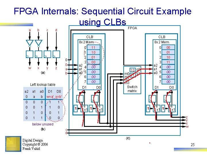
FPGA Internals: Sequential Circuit Example using CLBs a b c FPGA d CLB w x y 0 0 a b z (a) Left lookup table D 1 8 x 2 Mem. 0 1 2 3 a 2 4 a 1 a 0 5 6 7 11 10 01 00 00 00 D 1 a 2 a 1 a 0 0 a b 0 0 0 1 1 0 0 1 0 1 1 0 0 CLB D 0 10 o 0 m 0 11 o 1 m 2 m 3 Switch matrix 00 01 10 11 00 00 D 1 D 0 10 10 w=a' x=b' below unused (b) Digital Design Copyright © 2006 Frank Vahid 1 10 2 x 1 1 10 1 2 x 1 z y x w c d (c) a 25

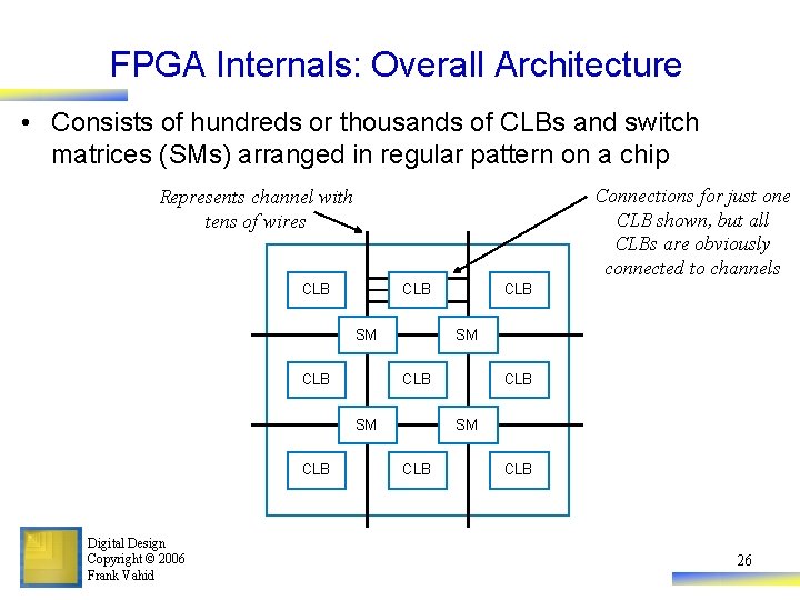
FPGA Internals: Overall Architecture • Consists of hundreds or thousands of CLBs and switch matrices (SMs) arranged in regular pattern on a chip Connections for just one CLB shown, but all CLBs are obviously connected to channels Represents channel with tens of wires CLB SM CLB Digital Design Copyright © 2006 Frank Vahid CLB SM CLB 26

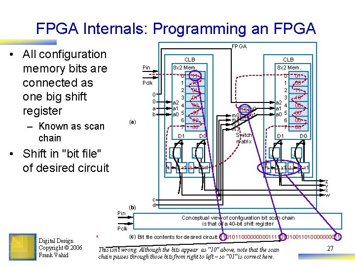
FPGA Internals: Programming an FPGA • All configuration memory bits are connected as one big shift register Pin Pclk 0 0 a b (a) – Known as scan chain • Shift in "bit file" of desired circuit 1 Pin Pclk Digital Design Copyright © 2006 Frank Vahid a CLB 8 x 2 Mem. 0 11 1 10 2 01 3 01 a 2 4 00 a 1 a 0 5 00 6 00 7 00 (b) D 1 D 0 2 x 1 1 2 x 1 CLB 8 x 2 Mem. 0 01 1 00 2 11 3 10 a 2 4 00 a 1 a 0 5 00 6 00 7 00 10 o 0 m 0 11 o 1 m 2 m 3 Switch matrix 1 D 0 2 x 1 1 2 x 1 z y x w c d Conceptual view of configuration bit scan chain is that of a 40 -bit shift register (c) Bit file contents for desired circuit: 11010110000011110101001101000011 This isn't wrong. Although the bits appear as "10" above, note that the scan chain passes through those bits from right to left – so "01" is correct here. 27

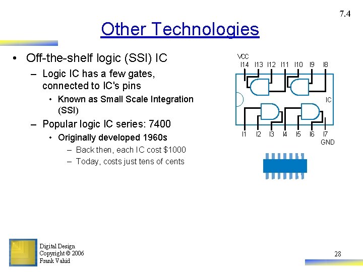
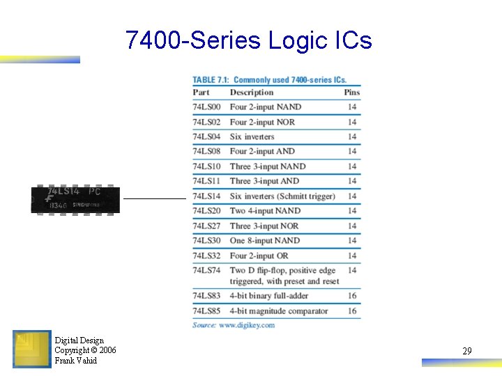
7. 4 Other Technologies • Off-the-shelf logic (SSI) IC – Logic IC has a few gates, connected to IC's pins VCC I 14 I 13 I 12 I 11 I 10 I 9 • Known as Small Scale Integration (SSI) I 8 IC – Popular logic IC series: 7400 • Originally developed 1960 s – Back then, each IC cost $1000 – Today, costs just tens of cents Digital Design Copyright © 2006 Frank Vahid I 1 I 2 I 3 I 4 I 5 I 6 I 7 GND 28

7400 -Series Logic ICs Digital Design Copyright © 2006 Frank Vahid 29

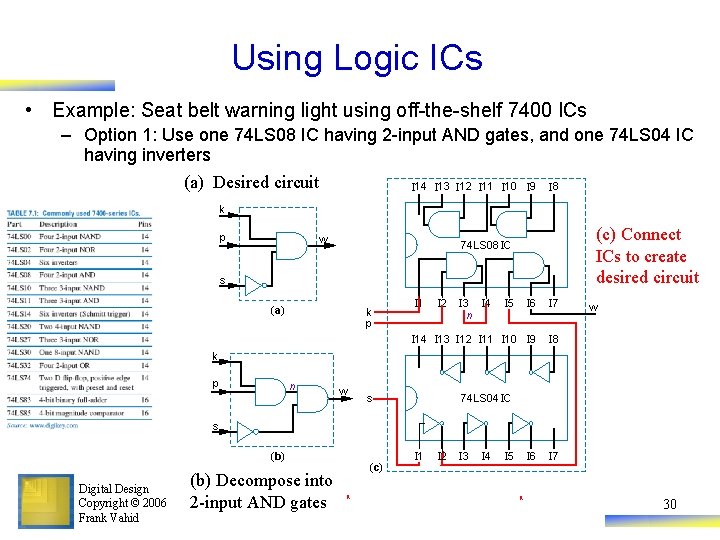
Using Logic ICs • Example: Seat belt warning light using off-the-shelf 7400 ICs – Option 1: Use one 74 LS 08 IC having 2 -input AND gates, and one 74 LS 04 IC having inverters (a) Desired circuit I 14 I 13 I 12 I 11 I 10 I 9 I 8 k p w (c) Connect ICs to create desired circuit 74 LS 08 IC s (a) k p I 1 I 2 I 3 I 4 n I 5 I 6 I 7 I 14 I 13 I 12 I 11 I 10 I 9 I 8 w k p n w s 74 LS 04 IC s (b) Digital Design Copyright © 2006 Frank Vahid (b) Decompose into 2 -input AND gates (c) a I 1 I 2 I 3 I 4 I 5 I 6 a I 7 30

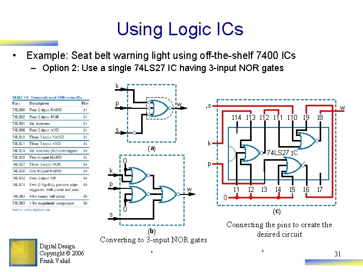
Using Logic ICs • Example: Seat belt warning light using off-the-shelf 7400 ICs – Option 2: Use a single 74 LS 27 IC having 3 -input NOR gates k p w s w I 14 I 13 I 12 I 11 I 10 I 9 I 8 s k (a) 74 LS 27 IC 0 p k p w I 1 I 2 I 3 I 4 I 5 I 6 I 7 0 s 0 (c) (b) Digital Design Copyright © 2006 Frank Vahid Converting to 3 -input NOR gates a Connecting the pins to create the desired circuit a 31

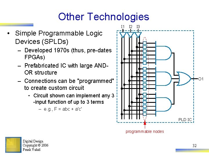
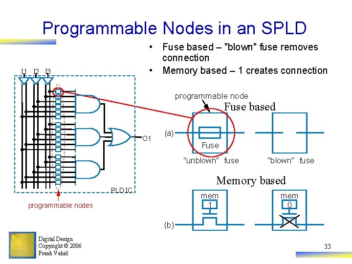
Other Technologies I 1 I 2 I 3 • Simple Programmable Logic Devices (SPLDs) – Developed 1970 s (thus, pre-dates FPGAs) – Prefabricated IC with large ANDOR structure – Connections can be "programmed" to create custom circuit O 1 • Circuit shown can implement any 3 -input function of up to 3 terms – e. g. , F = abc + a'c' PLD IC programmable nodes Digital Design Copyright © 2006 Frank Vahid 32

Programmable Nodes in an SPLD • Fuse based – "blown" fuse removes connection • Memory based – 1 creates connection I 1 I 2 I 3 programmable node Fuse based O 1 (a) Fuse "unblown" fuse "blown" fuse Memory based PLD IC mem 1 programmable nodes mem 0 (b) Digital Design Copyright © 2006 Frank Vahid 33

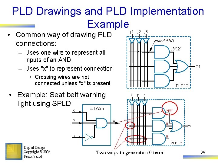
PLD Drawings and PLD Implementation Example I 1 I 2 I 3 • Common way of drawing PLD connections: wired AND × – Uses one wire to represent all inputs of an AND – Uses "x" to represent connection I 3*I 2' × O 1 • Crossing wires are not connected unless "x" is present PLD IC • Example: Seat belt warning light using SPLD k p s Belt. Warn × × × w ×× s ×× ×× ×× kps' 0 w 0 PLD IC Digital Design Copyright © 2006 Frank Vahid Two ways to generate a 0 term 34

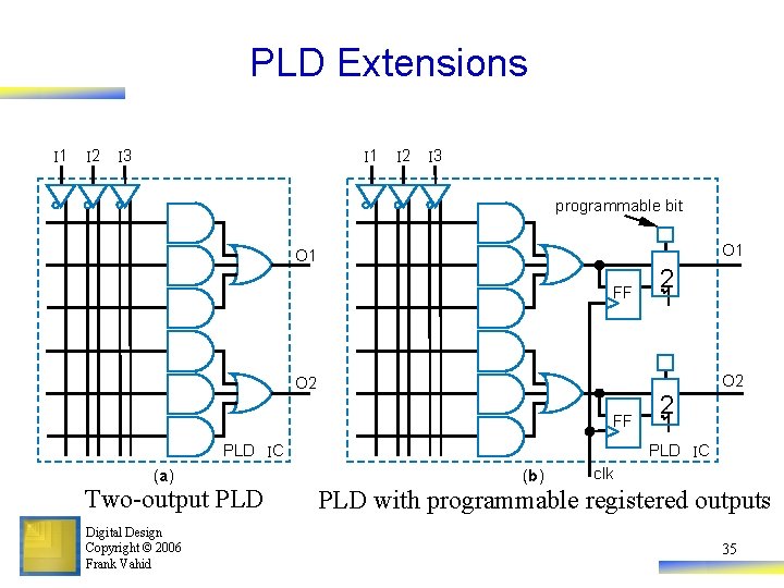
PLD Extensions I 1 I 2 I 3 programmable bit O 1 FF O 2 FF PLD IC (a ) Two-output PLD Digital Design Copyright © 2006 Frank Vahid 2 × 1 PLD IC (b ) clk PLD with programmable registered outputs 35

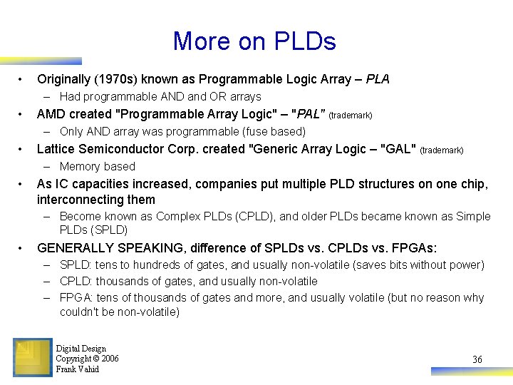
More on PLDs • Originally (1970 s) known as Programmable Logic Array – PLA – Had programmable AND and OR arrays • AMD created "Programmable Array Logic" – "PAL" (trademark) – Only AND array was programmable (fuse based) • Lattice Semiconductor Corp. created "Generic Array Logic – "GAL" (trademark) – Memory based • As IC capacities increased, companies put multiple PLD structures on one chip, interconnecting them – Become known as Complex PLDs (CPLD), and older PLDs became known as Simple PLDs (SPLD) • GENERALLY SPEAKING, difference of SPLDs vs. CPLDs vs. FPGAs: – SPLD: tens to hundreds of gates, and usually non-volatile (saves bits without power) – CPLD: thousands of gates, and usually non-volatile – FPGA: tens of thousands of gates and more, and usually volatile (but no reason why couldn't be non-volatile) Digital Design Copyright © 2006 Frank Vahid 36

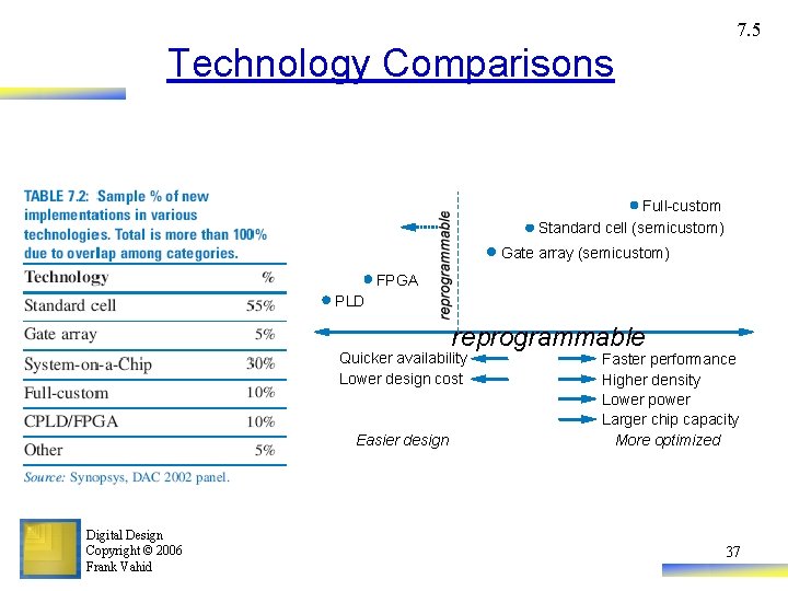
7. 5 Technology Comparisons Full-custom Standard cell (semicustom) Gate array (semicustom) FPGA PLD reprogrammable Quicker availability Lower design cost Easier design Digital Design Copyright © 2006 Frank Vahid Faster performance Higher density Lower power Larger chip capacity More optimized 37

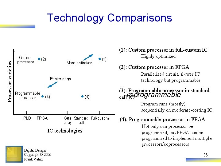
Technology Comparisons Processor varieties (1): Custom processor in full-custom IC Custom processor (2) More optimized (1) (4) (2): Custom processor in FPGA Parallelized circuit, slower IC technology but programmable Easier desi gn Programmable processor Highly optimized (3): Programmable processor in standard cellreprogrammable IC Program runs (mostly) sequentially on moderate-costing IC PLD FPGA Gate Standard Full-custom array cell IC technologies Digital Design Copyright © 2006 Frank Vahid (4): Programmable processor in FPGA Not only can processor be programmed, but FPGA can be programmed to implement multiple processors/coprocessors 38

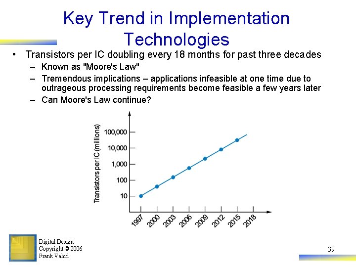
Key Trend in Implementation Technologies • Transistors per IC doubling every 18 months for past three decades – Known as "Moore's Law" – Tremendous implications – applications infeasible at one time due to outrageous processing requirements become feasible a few years later – Can Moore's Law continue? Digital Design Copyright © 2006 Frank Vahid 39

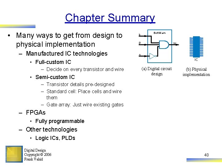
Chapter Summary • Many ways to get from design to physical implementation – Manufactured IC technologies k Belt Warn p w s IC • Full-custom IC – Decide on every transistor and wire • Semi-custom IC (a) Digital circuit design (b) Physical implementation – Transistor details pre-designed – Standard cell: Place cells and wire them – Gate array: Just wire existing gates – FPGAs • Fully programmable – Other technologies • Logic ICs, PLDs Digital Design Copyright © 2006 Frank Vahid 40