Digital Design Chapter 2 Combinational Logic Design Slides
Digital Design Chapter 2: Combinational Logic Design Slides to accompany the textbook Digital Design, First Edition, by Frank Vahid, John Wiley and Sons Publishers, 2007. Copyright © 2007 Frank Vahid Instructors of courses requiring Vahid's Digital Design textbook (published by John Wiley and Sons) have permission to modify and use these slides for customary course-related activities, subject to keeping this copyright notice in place and unmodified. These slides may be posted as unanimated pdf versions on publicly-accessible course websites. . Power. Point source (or pdf Digital Design with animations) may not be posted to publicly-accessible websites, but may be posted for students on internal protected sites or distributed directly to students by other electronic means. Copyright © 2006 1 Instructors may make printouts of the slides available to students for a reasonable photocopying charge, without incurring royalties. Any other use requires explicit permission. Instructors Franksource Vahid may obtain Power. Point or obtain special use permissions from Wiley – see http: //www. ddvahid. com for information.
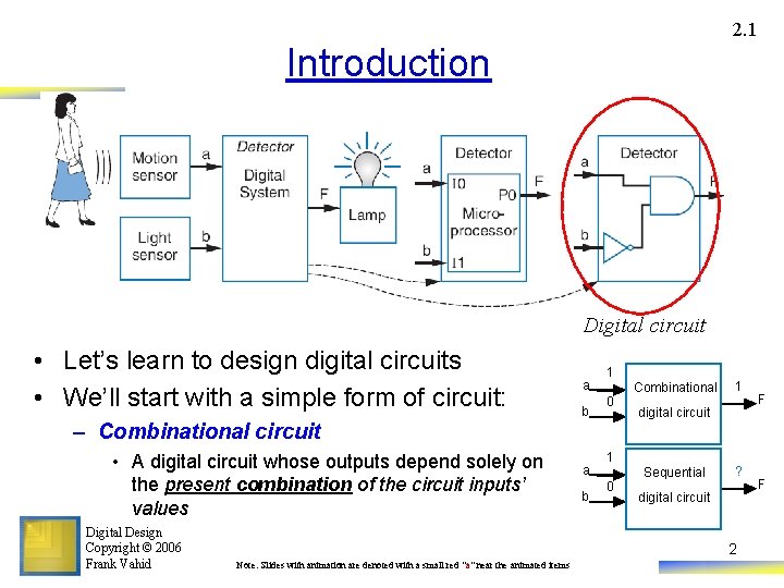
2. 1 Introduction Digital circuit • Let’s learn to design digital circuits • We’ll start with a simple form of circuit: a b 1 Combinational 0 – Combinational circuit • A digital circuit whose outputs depend solely on the present combination of the circuit inputs’ values Digital Design Copyright © 2006 Frank Vahid a b digital circuit 1 0 1 Sequential ? digital circuit 2 Note: Slides with animation are denoted with a small red "a" near the animated items F F
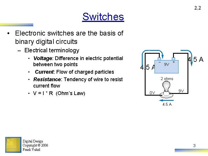
2. 2 Switches • Electronic switches are the basis of binary digital circuits – Electrical terminology • Voltage: Difference in electric potential between two points • Current: Flow of charged particles • Resistance: Tendency of wire to resist current flow • V = I * R (Ohm’s Law) 4. 5 A – 9 V 4. 5 A + 2 ohms 9 V 0 V 4. 5 A Digital Design Copyright © 2006 Frank Vahid 3
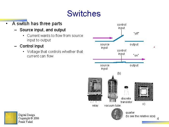
Switches • A switch has three parts control input – Source input, and output “off” • Current wants to flow from source input to output source input – Control input • Voltage that controls whether that current can flow output a control input source input “on” output (b) relay Digital Design Copyright © 2006 Frank Vahid discrete transistor vacuum tube IC quarter (to see the relative size) 4
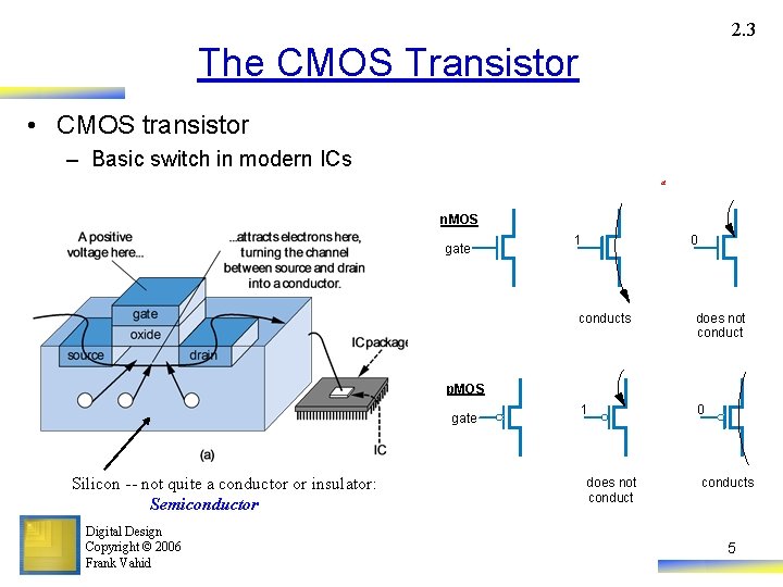
2. 3 The CMOS Transistor • CMOS transistor – Basic switch in modern ICs a n. MOS gate 1 0 conducts does not conduct 1 0 p. MOS gate Silicon -- not quite a conductor or insulator: Semiconductor Digital Design Copyright © 2006 Frank Vahid does not conducts 5
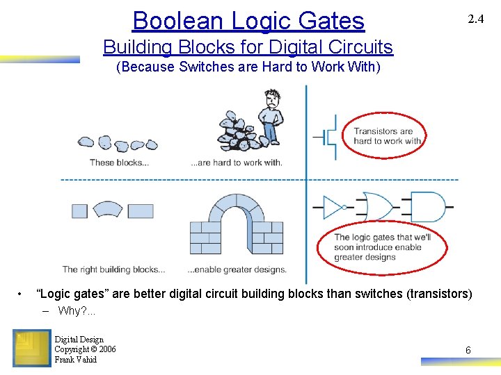
Boolean Logic Gates 2. 4 Building Blocks for Digital Circuits (Because Switches are Hard to Work With) • “Logic gates” are better digital circuit building blocks than switches (transistors) – Why? . . . Digital Design Copyright © 2006 Frank Vahid 6
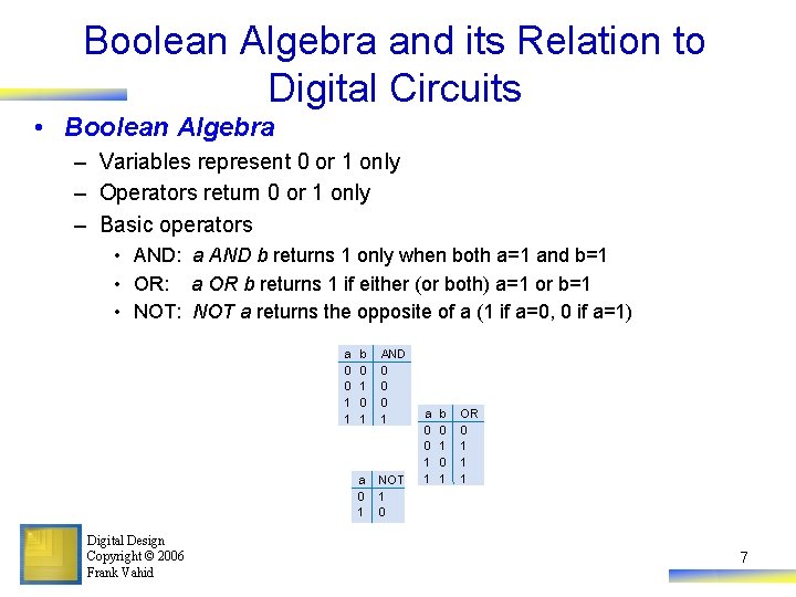
Boolean Algebra and its Relation to Digital Circuits • Boolean Algebra – Variables represent 0 or 1 only – Operators return 0 or 1 only – Basic operators • AND: a AND b returns 1 only when both a=1 and b=1 • OR: a OR b returns 1 if either (or both) a=1 or b=1 • NOT: NOT a returns the opposite of a (1 if a=0, 0 if a=1) a 0 0 1 1 Digital Design Copyright © 2006 Frank Vahid b 0 1 AND 0 0 0 1 a 0 1 NOT 1 0 a 0 0 1 1 b 0 1 OR 0 1 1 1 7
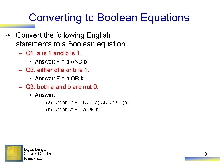
Converting to Boolean Equations a • Convert the following English statements to a Boolean equation – Q 1. a is 1 and b is 1. • Answer: F = a AND b – Q 2. either of a or b is 1. • Answer: F = a OR b – Q 3. both a and b are not 0. • Answer: – (a) Option 1: F = NOT(a) AND NOT(b) – (b) Option 2: F = a OR b Digital Design Copyright © 2006 Frank Vahid 8
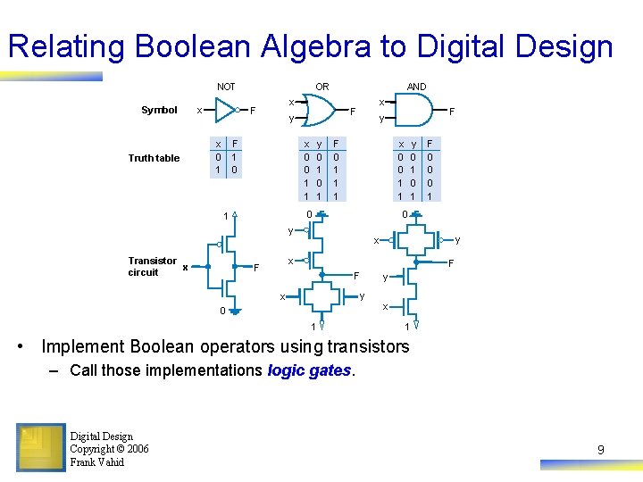
Relating Boolean Algebra to Digital Design NOT Symbol Truth table x OR x F x 0 1 AND y F 1 0 x F x 0 0 1 1 y 0 1 F 0 1 1 1 x 0 0 1 1 0 1 y x x F F 0 0 0 1 0 y Transistor x circuit F y F F y x 0 1 y x 1 • Implement Boolean operators using transistors – Call those implementations logic gates. Digital Design Copyright © 2006 Frank Vahid 9
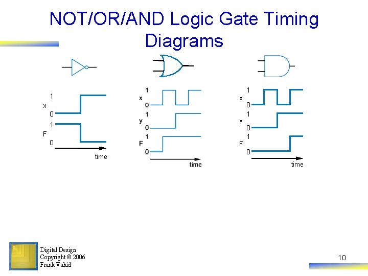
NOT/OR/AND Logic Gate Timing Diagrams 1 1 x x 0 y 1 F 0 F time 0 1 0 time Digital Design Copyright © 2006 Frank Vahid 10
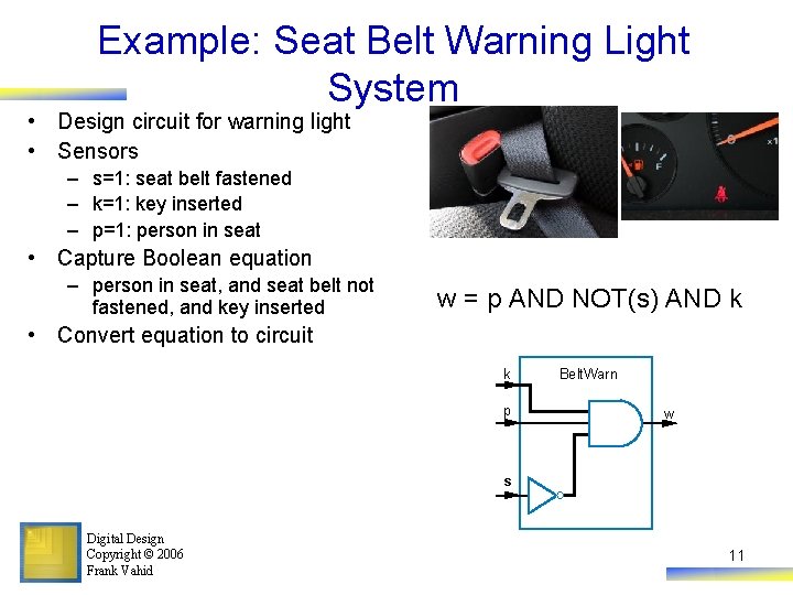
Example: Seat Belt Warning Light System • Design circuit for warning light • Sensors – s=1: seat belt fastened – k=1: key inserted – p=1: person in seat • Capture Boolean equation – person in seat, and seat belt not fastened, and key inserted w = p AND NOT(s) AND k • Convert equation to circuit k p Belt. Warn w s Digital Design Copyright © 2006 Frank Vahid 11
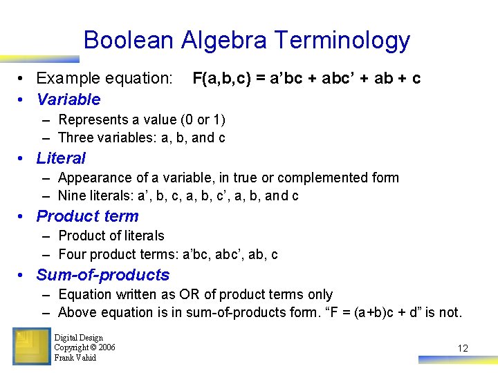
Boolean Algebra Terminology • Example equation: • Variable F(a, b, c) = a’bc + abc’ + ab + c – Represents a value (0 or 1) – Three variables: a, b, and c • Literal – Appearance of a variable, in true or complemented form – Nine literals: a’, b, c, a, b, c’, a, b, and c • Product term – Product of literals – Four product terms: a’bc, abc’, ab, c • Sum-of-products – Equation written as OR of product terms only – Above equation is in sum-of-products form. “F = (a+b)c + d” is not. Digital Design Copyright © 2006 Frank Vahid 12
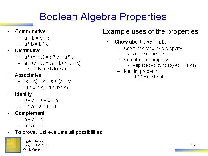
Boolean Algebra Properties • Commutative – a+b=b+a – a*b=b*a • Distributive – a * (b + c) = a * b + a * c – a + (b * c) = (a + b) * (a + c) • (this one is tricky!) • Associative – (a + b) + c = a + (b + c) – (a * b) * c = a * (b * c) • Example uses of the properties • Show abc + abc’ = ab. – Use first distributive property • abc + abc’ = ab(c+c’). – Complement property • Replace c+c’ by 1: ab(c+c’) = ab(1). – Identity property • ab(1) = ab*1 = ab. Identity – 0+a=a+0=a – 1*a=a*1=a • Complement – a + a’ = 1 – a * a’ = 0 • To prove, just evaluate all possibilities Digital Design Copyright © 2006 Frank Vahid 13
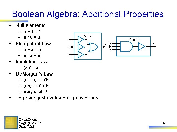
Boolean Algebra: Additional Properties • Null elements – a+1=1 – a*0=0 • Idempotent Law – a+a=a – a*a=a Circuit a b S a b c S c • Involution Law – (a’)’ = a • De. Morgan’s Law – (a + b)’ = a’b’ – (ab)’ = a’ + b’ – Very useful! • To prove, just evaluate all possibilities Digital Design Copyright © 2006 Frank Vahid 14
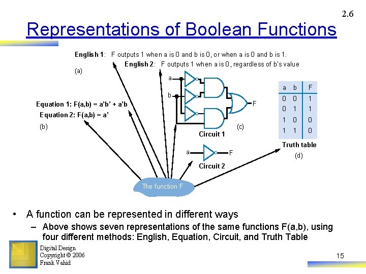
2. 6 Representations of Boolean Functions English 1: F outputs 1 when a is 0 and b is 0, or when a is 0 and b is 1. (a) English 2: F outputs 1 when a is 0, regardless of b’s value a b F Equation 1: F(a, b) = a’b’ + a’b Equation 2: F(a, b) = a’ (c) (b) Circuit 1 a b F 0 0 1 1 1 0 0 1 1 0 Truth table a F (d) Circuit 2 The function F • A function can be represented in different ways – Above shows seven representations of the same functions F(a, b), using four different methods: English, Equation, Circuit, and Truth Table Digital Design Copyright © 2006 Frank Vahid 15
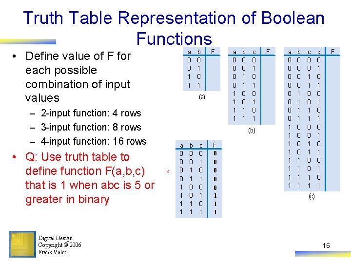
Truth Table Representation of Boolean Functions a 0 0 1 1 • Define value of F for each possible combination of input values Digital Design Copyright © 2006 Frank Vahid F (a) – 2 -input function: 4 rows – 3 -input function: 8 rows – 4 -input function: 16 rows • Q: Use truth table to define function F(a, b, c) that is 1 when abc is 5 or greater in binary b 0 1 a 0 0 1 1 b 0 0 1 1 c 0 1 0 1 (b) a a 0 0 1 1 b 0 0 1 1 c 0 1 0 1 F 0 0 0 1 1 1 F a 0 0 0 0 1 1 1 1 b 0 0 0 0 1 1 1 1 c 0 0 1 1 d 0 1 0 1 (c) 16 F
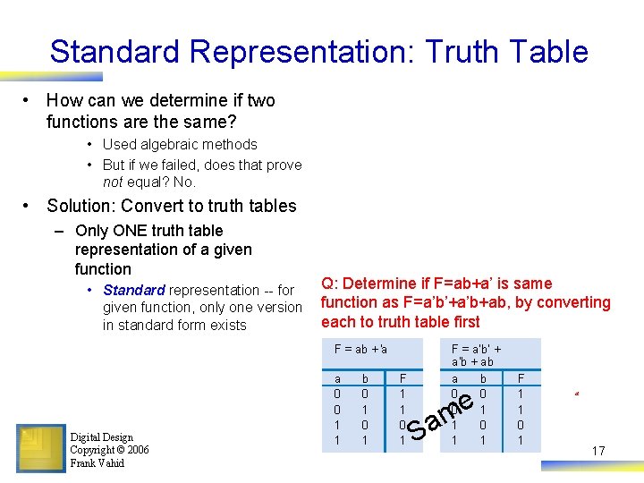
Standard Representation: Truth Table • How can we determine if two functions are the same? • Used algebraic methods • But if we failed, does that prove not equal? No. • Solution: Convert to truth tables – Only ONE truth table representation of a given function • Standard representation -- for given function, only one version in standard form exists Q: Determine if F=ab+a’ is same function as F=a’b’+a’b+ab, by converting each to truth table first F = ab + 'a Digital Design Copyright © 2006 Frank Vahid a 0 0 1 1 b 0 1 F = a’b’ + a’b + ab F 1 1 0 1 a 0 0 1 1 S e m a b 0 1 F 1 1 0 1 a 17
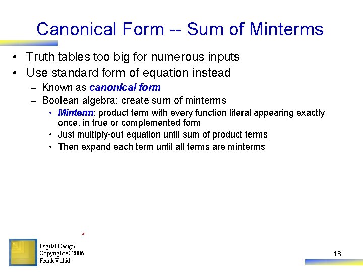
Canonical Form -- Sum of Minterms • Truth tables too big for numerous inputs • Use standard form of equation instead – Known as canonical form – Boolean algebra: create sum of minterms • Minterm: product term with every function literal appearing exactly once, in true or complemented form • Just multiply-out equation until sum of product terms • Then expand each term until all terms are minterms a Digital Design Copyright © 2006 Frank Vahid 18
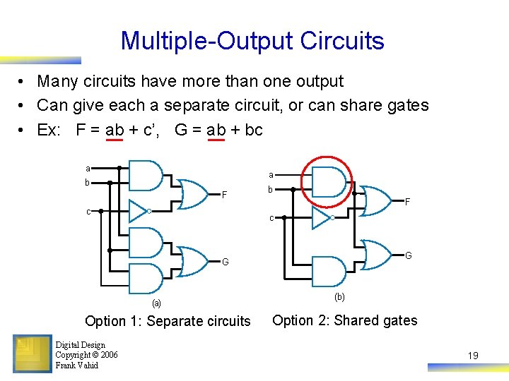
Multiple-Output Circuits • Many circuits have more than one output • Can give each a separate circuit, or can share gates • Ex: F = ab + c’, G = ab + bc a a b F c G G (a) Option 1: Separate circuits Digital Design Copyright © 2006 Frank Vahid (b) Option 2: Shared gates 19
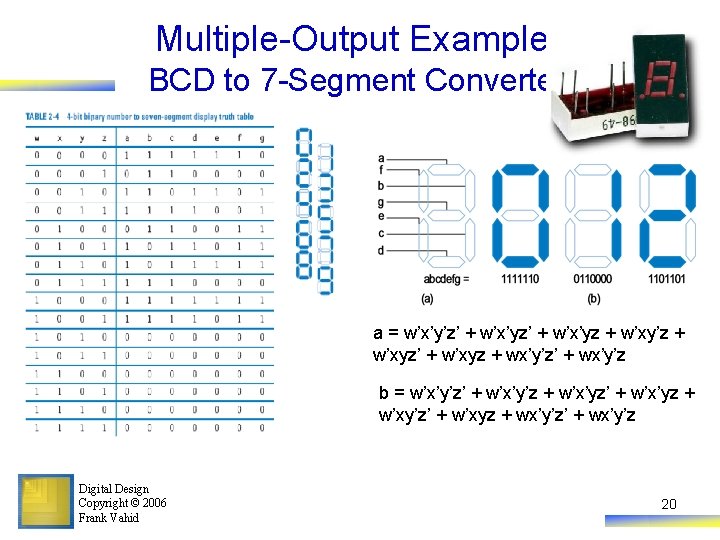
Multiple-Output Example: BCD to 7 -Segment Converter a = w’x’y’z’ + w’x’yz + w’xy’z + w’xyz’ + w’xyz + wx’y’z’ + wx’y’z b = w’x’y’z’ + w’x’y’z + w’x’yz’ + w’x’yz + w’xy’z’ + w’xyz + wx’y’z’ + wx’y’z Digital Design Copyright © 2006 Frank Vahid 20
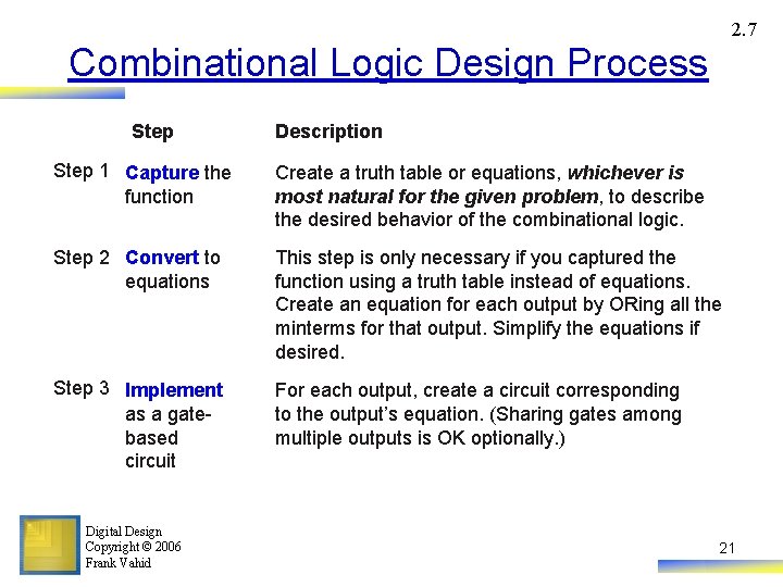
2. 7 Combinational Logic Design Process Step Description Step 1 Capture the function Create a truth table or equations, whichever is most natural for the given problem, to describe the desired behavior of the combinational logic. Step 2 Convert to equations This step is only necessary if you captured the function using a truth table instead of equations. Create an equation for each output by ORing all the minterms for that output. Simplify the equations if desired. Step 3 Implement as a gatebased circuit For each output, create a circuit corresponding to the output’s equation. (Sharing gates among multiple outputs is OK optionally. ) Digital Design Copyright © 2006 Frank Vahid 21
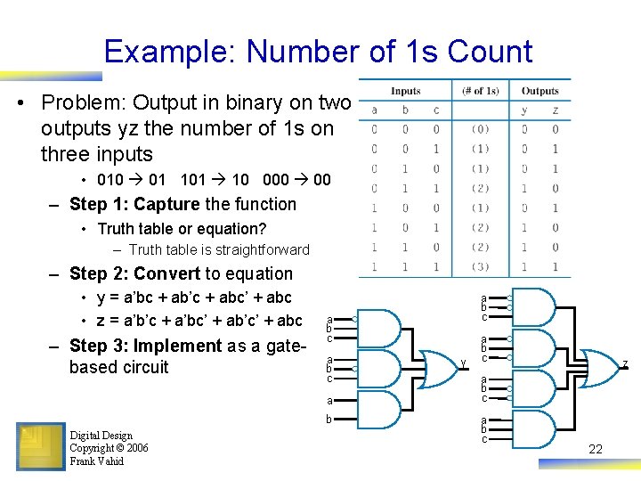
Example: Number of 1 s Count • Problem: Output in binary on two outputs yz the number of 1 s on three inputs • 010 01 101 10 000 00 – Step 1: Capture the function • Truth table or equation? – Truth table is straightforward – Step 2: Convert to equation • y = a’bc + ab’c + abc’ + abc • z = a’b’c + a’bc’ + ab’c’ + abc – Step 3: Implement as a gatebased circuit a b c a b Digital Design Copyright © 2006 Frank Vahid a b c y a b c z a b c 22
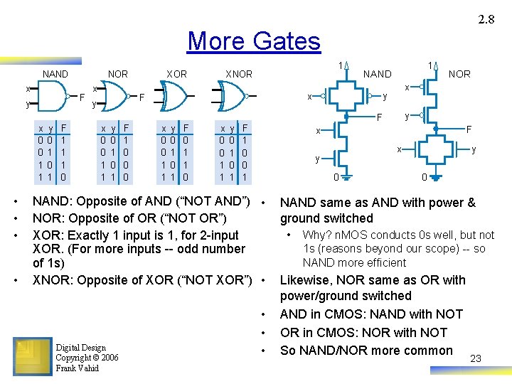
2. 8 More Gates NAND x NOR F y x XOR 1 XNOR y F x 0 0 1 1 • • y 0 1 F 1 1 1 0 x 0 0 1 1 y 0 1 F 1 0 0 0 x 0 0 1 1 y 0 1 F 0 1 1 0 x 0 0 1 1 y 0 1 F 1 0 0 1 F x 0 • • • y x y NAND: Opposite of AND (“NOT AND”) • NOR: Opposite of OR (“NOT OR”) XOR: Exactly 1 input is 1, for 2 -input XOR. (For more inputs -- odd number of 1 s) XNOR: Opposite of XOR (“NOT XOR”) • Digital Design Copyright © 2006 Frank Vahid NOR x y x F y 1 NAND 0 NAND same as AND with power & ground switched • Why? n. MOS conducts 0 s well, but not 1 s (reasons beyond our scope) -- so NAND more efficient Likewise, NOR same as OR with power/ground switched AND in CMOS: NAND with NOT OR in CMOS: NOR with NOT So NAND/NOR more common 23
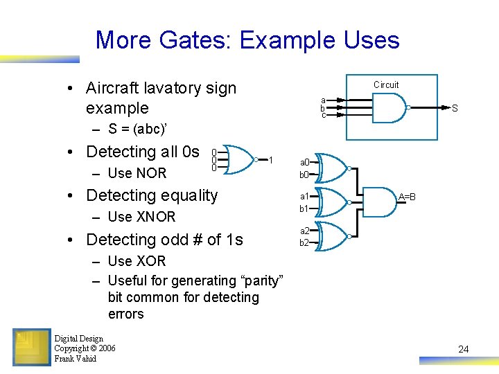
More Gates: Example Uses • Aircraft lavatory sign example Circuit a b c S – S = (abc)’ • Detecting all 0 s – Use NOR 0 0 0 1 • Detecting equality – Use XNOR • Detecting odd # of 1 s a 0 b 0 a 1 b 1 A=B a 2 b 2 – Use XOR – Useful for generating “parity” bit common for detecting errors Digital Design Copyright © 2006 Frank Vahid 24
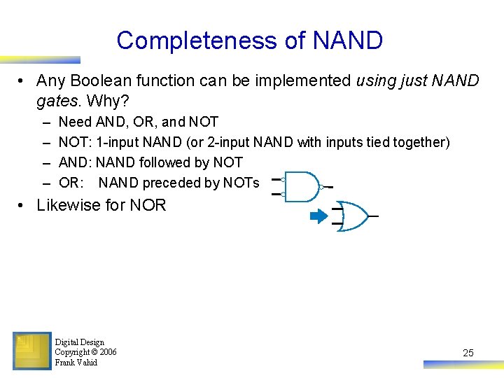
Completeness of NAND • Any Boolean function can be implemented using just NAND gates. Why? – – Need AND, OR, and NOT: 1 -input NAND (or 2 -input NAND with inputs tied together) AND: NAND followed by NOT OR: NAND preceded by NOTs • Likewise for NOR Digital Design Copyright © 2006 Frank Vahid 25
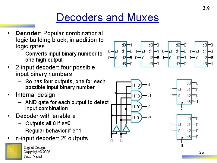
2. 9 Decoders and Muxes • Decoder: Popular combinational logic building block, in addition to logic gates – Converts input binary number to one high output d 0 0 i 0 d 1 0 1 i 0 d 1 1 0 i 0 d 1 0 1 i 0 d 1 0 0 i 1 d 2 0 1 i 1 d 2 1 1 i 1 d 2 0 d 3 1 d 3 – So has four outputs, one for each possible input binary number • Internal design – AND gate for each output to detect input combination • Decoder with enable e – Outputs all 0 if e=0 – Regular behavior if e=1 Digital Design Copyright © 2006 Frank Vahid d 0 0 • 2 -input decoder: four possible input binary numbers • n-input decoder: 2 n outputs d 0 1 i 0 0 d 3 i 1’i 0’ d 0 i 1’i 0 d 1 i 1 i 0’ d 2 i 1 i 0 d 3 0 d 0 0 1 i 0 d 1 0 1 i 1 d 2 0 e d 3 1 1 d 0 0 1 i 0 d 1 0 1 i 1 d 2 0 e d 3 0 0 26
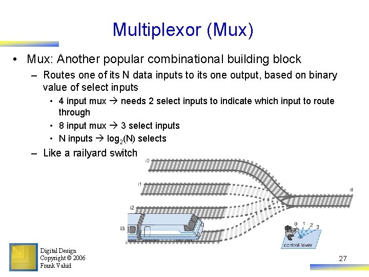
Multiplexor (Mux) • Mux: Another popular combinational building block – Routes one of its N data inputs to its one output, based on binary value of select inputs • 4 input mux needs 2 select inputs to indicate which input to route through • 8 input mux 3 select inputs • N inputs log 2(N) selects – Like a railyard switch Digital Design Copyright © 2006 Frank Vahid 27
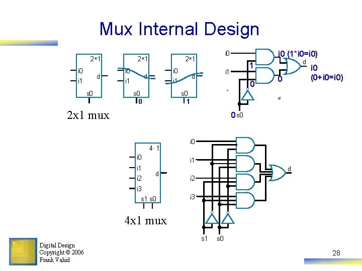
Mux Internal Design 2× 1 i 0 d i 1 s 0 0 d 1 i 1 d i 1 i 0 (1*i 0=i 0) i 0 2× 1 0 s 0 1 0 i 0 (0+i 0=i 0) a 2 x 1 mux 0 s 0 4× 1 i 0 i 1 i 2 i 0 i 1 d d i 2 i 3 s 1 s 0 i 3 4 x 1 mux Digital Design Copyright © 2006 Frank Vahid s 1 s 0 28
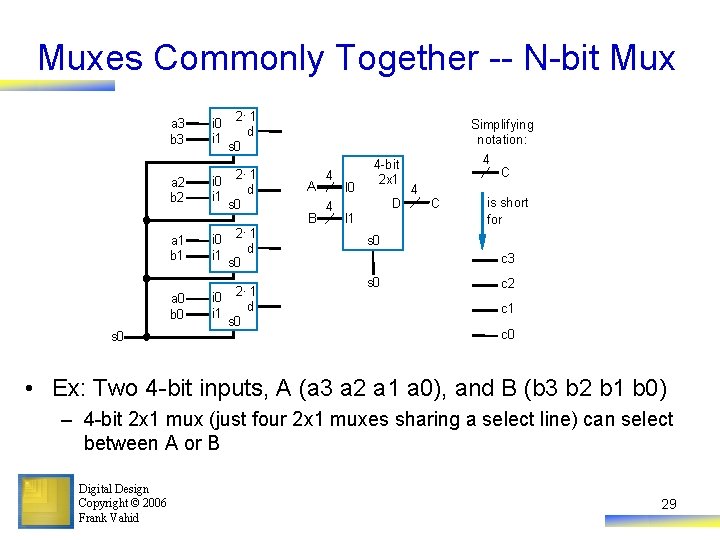
Muxes Commonly Together -- N-bit Mux s 0 2× 1 d s 0 a 3 b 3 i 0 i 1 a 2 b 2 2× 1 i 0 d i 1 s 0 2× 1 d s 0 a 1 b 1 i 0 i 1 a 0 b 0 × i 0 2 1 d i 1 s 0 A B 4 4 I 0 4 -bit 2 x 1 D I 1 Simplifying notation: 4 C is short for s 0 c 3 s 0 c 2 c 1 c 0 • Ex: Two 4 -bit inputs, A (a 3 a 2 a 1 a 0), and B (b 3 b 2 b 1 b 0) – 4 -bit 2 x 1 mux (just four 2 x 1 muxes sharing a select line) can select between A or B Digital Design Copyright © 2006 Frank Vahid 29
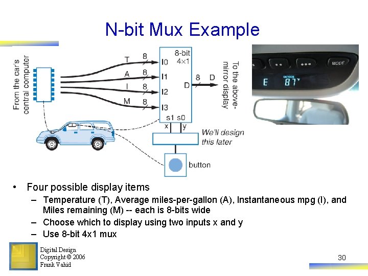
N-bit Mux Example • Four possible display items – Temperature (T), Average miles-per-gallon (A), Instantaneous mpg (I), and Miles remaining (M) -- each is 8 -bits wide – Choose which to display using two inputs x and y – Use 8 -bit 4 x 1 mux Digital Design Copyright © 2006 Frank Vahid 30
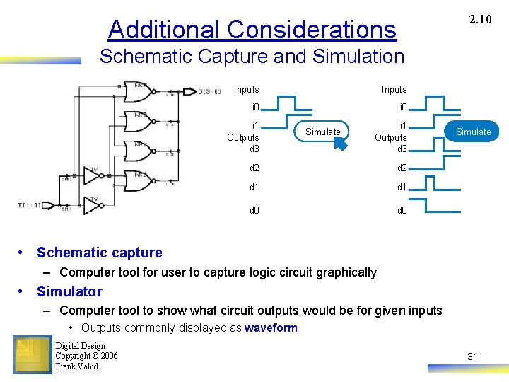
2. 10 Additional Considerations Schematic Capture and Simulation Inputs i 0 i 1 Outputs d 3 Simulate i 1 Outputs d 3 d 2 d 1 d 0 Simulate • Schematic capture – Computer tool for user to capture logic circuit graphically • Simulator – Computer tool to show what circuit outputs would be for given inputs • Outputs commonly displayed as waveform Digital Design Copyright © 2006 Frank Vahid 31
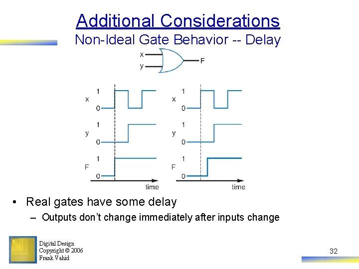
Additional Considerations Non-Ideal Gate Behavior -- Delay • Real gates have some delay – Outputs don’t change immediately after inputs change Digital Design Copyright © 2006 Frank Vahid 32
Chapter Summary • Combinational circuits – Circuit whose outputs are function of present inputs • No “state” • Switches: Basic component in digital circuits • Boolean logic gates: AND, OR, NOT -- Better building block than switches – Enables use of Boolean algebra to design circuits • Boolean algebra: uses true/false variables/operators • Representations of Boolean functions: Can translate among • Combinational design process: Translate from equation (or table) to circuit through well-defined steps • More gates: NAND, NOR, XNOR also useful • Muxes and decoders: Additional useful combinational building blocks Digital Design Copyright © 2006 Frank Vahid 33
- Slides: 33