Digital Decode Correction Logic Preliminary design review PAYAL


 decisions Correct ADC")


- Slides: 24
Digital Decode & Correction Logic Preliminary design review PAYAL DAVE
Outline • Introduction • Why Digital Decode & Error correction logic requires • Main Block diagram • Individual block explanation • Sims result • Conclusion
A 7 D 7 B 7 A 6 D 6 B 6 A 5 D 5 B 5
Need for Digital Decode & Error Correction • To eliminate the redundancy of ½ bit in each stage • Digital correction takes raw output data of the ADC as input and outputs the digital representation. • Error correction logic circuitry takes 14 bit input from ADC stages and eliminated the redundancy of ½ bit in each stage and gives 8 bit digital output. • Digital circuits are fast and take low power.
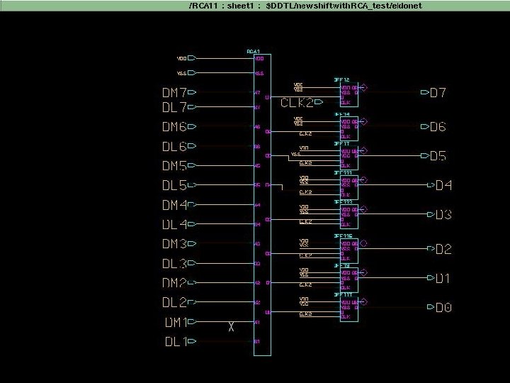
How it is done? • Requirements: § § Align ADC (comparator) decisions Correct ADC output bit pattern Add digital data in a 1. 5 -bit fashion Output a 8 -bit digital word • Implementation: § Shift register using Delayed D flip flop § Ripple carry adder
Main Block Diagram A 7 B 7 A 6 B 6 A 5 B 5 A 4 B 4 A 3 B 3 A 2 B 2 A 1 B 1 CLK 2 SHIFT REGISTER Ripple Carry Adder CLK 2 Output register D 7 D 6 D 5 D 4 D 3 D 2 D 1 D 0
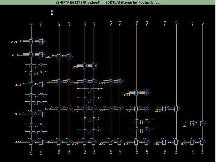
Shift register to align ADC decisions STG -1 CLK 1 DFF CLK 2 DFF STG -2 STG -4 STG -6 Shift register using D flipflop DFF DFF DFF CLK 1 CLK 2 STG -7 DFF CLK 1 CLK 2 STG -5 DFF CLK 1 CLK 2 STG -3 DFF DFF DFF RIPPLE CARRY ADDER DFF
SHIFT REGISTER TEST BENCH SHIFT REG
ALIGNING OF 14 BITS WITHIN 31/2 CLK
Digital correction logic A 7 A 6 B 6 A 5 STAGE - 3 B 5 B 4 A 4 Concept of Digital Correction + STAGE - 1 STAGE - 2 B 7 A 3 STAGE -4 B 3 A 2 D 7 D 6 D 5 D 4 D 3 * Z = D Y = B XOR C X = A + BC (CARRY BIT) * D 2 STAGE - 5 STAGE -6 B 2 A 1 B 1 D 1 STAGE 7 D 0 * A B C D Y Z + Mathematical analysis Of Digital Correction X
Logic Equations used for RCA • Total gate delay for RCA C 0 = A 2 + A 1 B 2 C 1 = B 3 C 0 + A 3 C 2 = B 4 C 1 + A 4 C 3 = B 5 C 2 + A 5 C 4 = B 6 C 3 + A 6 D 0 = B 1 D 1 = A 1 XOR B 2 D 2 = C 0 XOR B 3 D 3 = C 1 XOR B 4 D 4 = C 2 XOR B 5 D 5 = C 3 XOR B 6 D 6 = C 4 XOR B 7 D 7 = B 7 C 4 + A 7
RIPPLE CARRY ADDER CARRY BIT A + BC
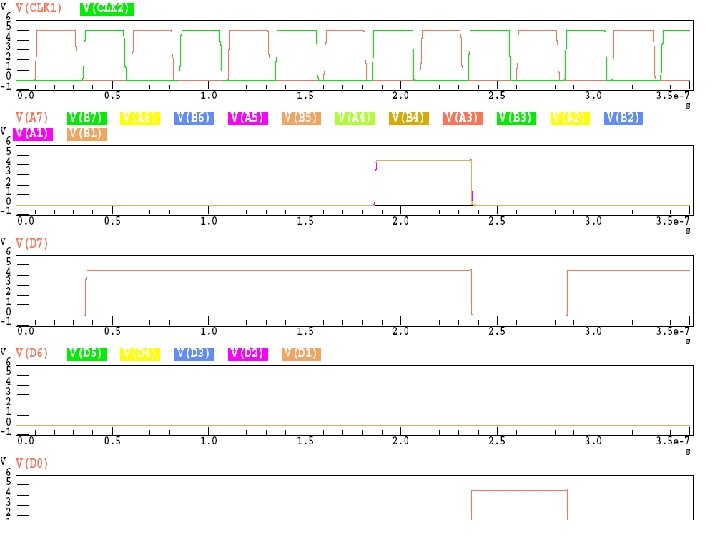
SS With worst case for 4. 5 v & 85 C
The delay in SS with worst case is 6. 34 ns
SIMS RESULTS FOR DIFFERENT CORNERS FOR RCA 5. 5 v 0 27 5. 0 v 85 0 27 4. 5 v 85 0 TT SS FS FF SF 4. 26 n 4. 63 n 5. 44 n 4. 94 n 3. 70 n 2. 69 n 27 85 3. 97 n 4. 65 n 5. 38 n 6. 34 n 4. 02 n 4. 73 n 2. 89 n 3. 36 n 3. 92 n 4. 60 n
ALIGNING OF 14 BITS WITHIN 31/2 CLK
Error Correction Logic A 7 B 7 A 6 B 6 A 5 B 5 A 6 B 6 A 4 B 4 A 3 B 3 A 2 B 2 A 1 B 1 01 01 D 7 D 6 D 5 D 4 D 3 D 2 D 1 D 0 01 1 1 1 1 01 01 10 000000 00 11 11 00000001 10 10 01111110 10 01 01111101
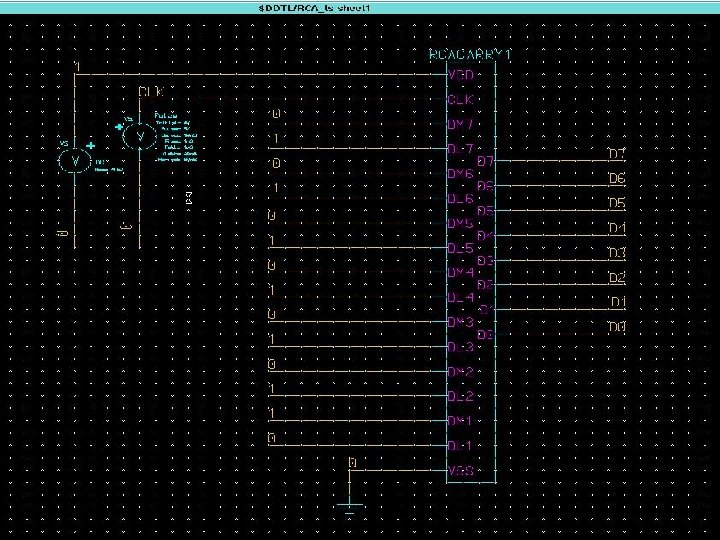
SHIFT REGISTER WITH RCA AND OUTPUT REGISTER SHIFT REGISTER RCA WITH OUTPUT REG
30 n 35 n Pulse width linear input to shift reg
Conclusion • 14 bits coming from the comparator are aligning with the help of the shift register within 41/2 clock cycle. • Ripple carry adder takes 6. 34 ns for worst case condition which is fast enough to get desired output • Error correction logic is working for different combination of input bits.