Diffusion and Ion Implantation SEMICONDUCTOR DOPING Diffusion and


- Slides: 24

Diffusion and Ion Implantation

SEMICONDUCTOR DOPING • • Diffusion and ion implantation are the two key processes used to introduce controlled amounts of dopants into semiconductors. They are used to selectively dope the semiconductor substrate to produce either an n-type or p-type region. In the diffusion method the dopant atoms are placed on the surface of the semiconductor by deposition from the gas phase of the dopant or by using doped-oxide sources. In ion implantation method the dopant ions are implanted into the semiconductor by means of a high energy ion beam.

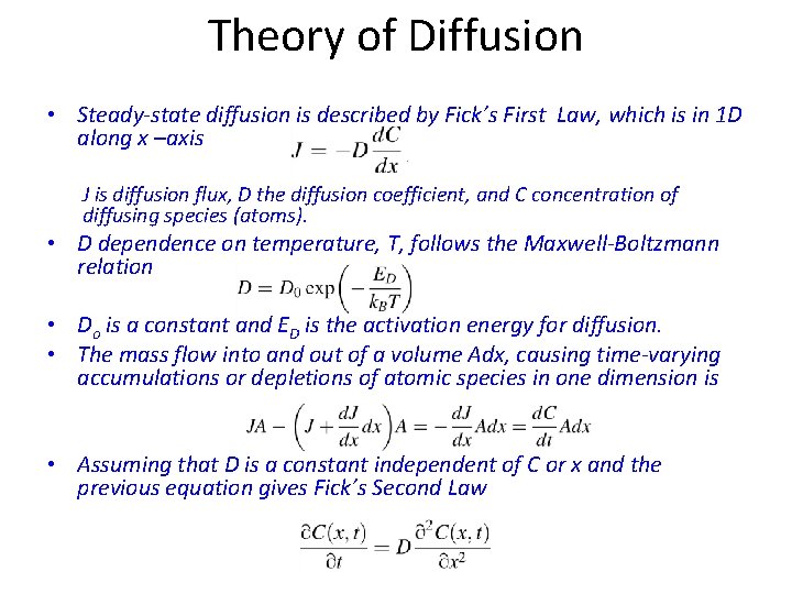
Theory of Diffusion • Steady-state diffusion is described by Fick’s First Law, which is in 1 D along x –axis J is diffusion flux, D the diffusion coefficient, and C concentration of diffusing species (atoms). • D dependence on temperature, T, follows the Maxwell-Boltzmann relation • Do is a constant and ED is the activation energy for diffusion. • The mass flow into and out of a volume Adx, causing time-varying accumulations or depletions of atomic species in one dimension is • Assuming that D is a constant independent of C or x and the previous equation gives Fick’s Second Law

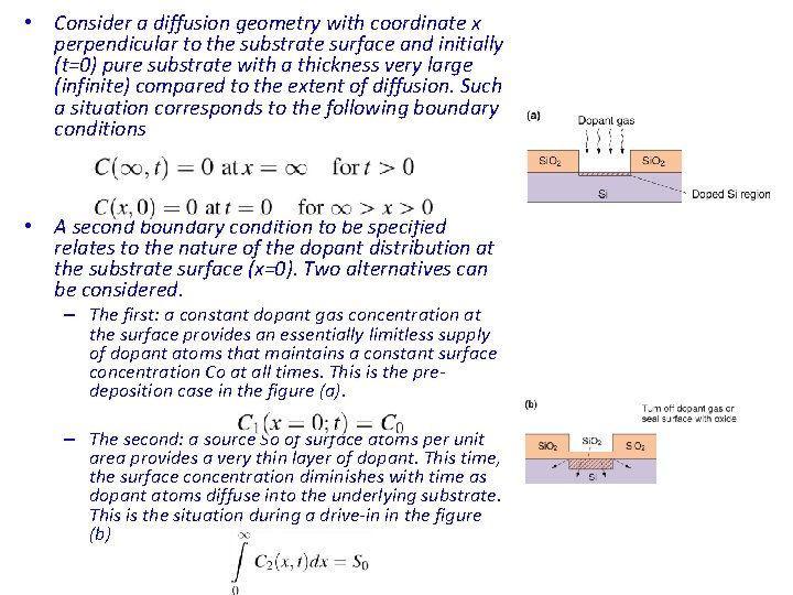
• Consider a diffusion geometry with coordinate x perpendicular to the substrate surface and initially (t=0) pure substrate with a thickness very large (infinite) compared to the extent of diffusion. Such a situation corresponds to the following boundary conditions • A second boundary condition to be specified relates to the nature of the dopant distribution at the substrate surface (x=0). Two alternatives can be considered. – The first: a constant dopant gas concentration at the surface provides an essentially limitless supply of dopant atoms that maintains a constant surface concentration Co at all times. This is the predeposition case in the figure (a). – The second: a source So of surface atoms per unit area provides a very thin layer of dopant. This time, the surface concentration diminishes with time as dopant atoms diffuse into the underlying substrate. This is the situation during a drive-in in the figure (b)

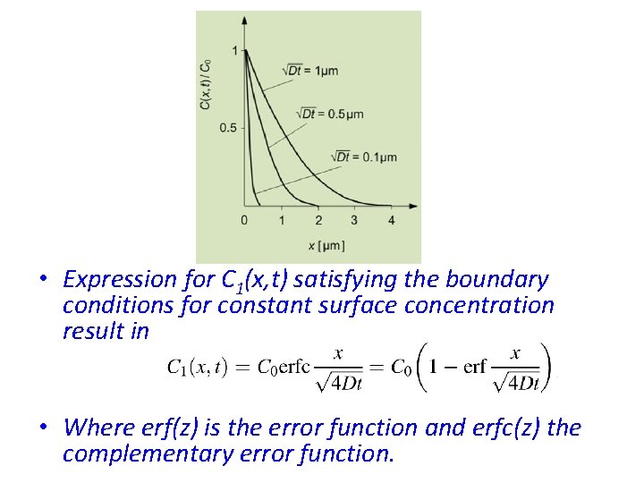
• Expression for C 1(x, t) satisfying the boundary conditions for constant surface concentration result in • Where erf(z) is the error function and erfc(z) the complementary error function.

• A diminishing concentration (drive-in profile) yields C 2(x, t) where So is the pre-deposition dose.

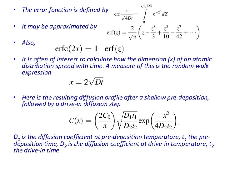
• The error function is defined by • It may be approximated by • Also, • It is often of interest to calculate how the dimension (x) of an atomic distribution spread with time. A measure of this is the random walk expression • Here is the resulting diffusion profile after a shallow pre-deposition, followed by a drive-in diffusion step D 1 is the diffusion coefficient at pre-deposition temperature, t 1 the predeposition time, D 2 is the diffusion coefficient at drive-in temperature, t 2 the drive-in time

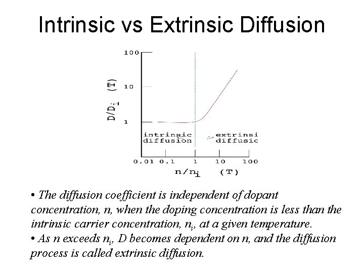
Intrinsic vs Extrinsic Diffusion • The diffusion coefficient is independent of dopant concentration, n, when the doping concentration is less than the intrinsic carrier concentration, ni, at a given temperature. • As n exceeds ni, D becomes dependent on n, and the diffusion process is called extrinsic diffusion.

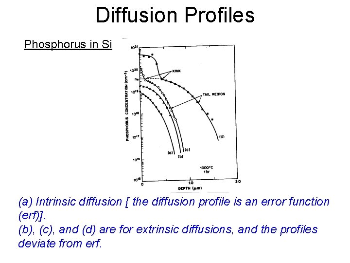
Diffusion Profiles Phosphorus in Si (a) Intrinsic diffusion [ the diffusion profile is an error function (erf)]. (b), (c), and (d) are for extrinsic diffusions, and the profiles deviate from erf.

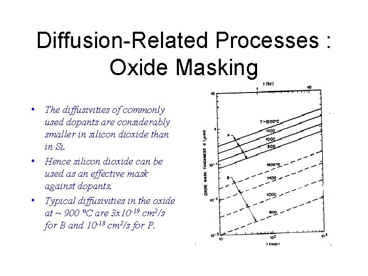
Diffusion-Related Processes : Oxide Masking • The diffusivities of commonly used dopants are considerably smaller in silicon dioxide than in Si. • Hence silicon dioxide can be used as an effective mask against dopants. • Typical diffusivities in the oxide at ~ 900 °C are 3 x 10 -19 cm 2/s for B and 10 -18 cm 2/s for P.

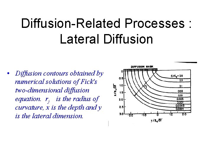
Diffusion-Related Processes : Lateral Diffusion • Diffusion contours obtained by numerical solutions of Fick's two-dimensional diffusion equation. rj is the radius of curvature, x is the depth and y is the lateral dimension.

A Typical Diffusion Process

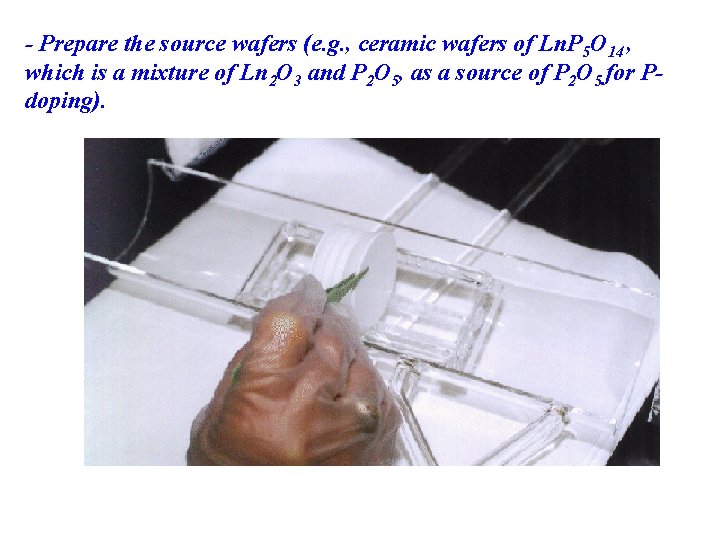
- Prepare the source wafers (e. g. , ceramic wafers of Ln. P 5 O 14 , which is a mixture of Ln 2 O 3 and P 2 O 5, as a source of P 2 O 5 for Pdoping).

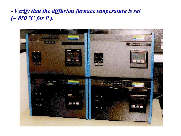
- Verify that the diffusion furnace temperature is set (~ 850 °C for P ).

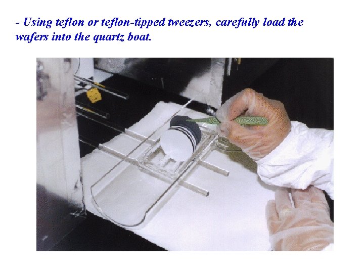
- Using teflon or teflon-tipped tweezers, carefully load the wafers into the quartz boat.

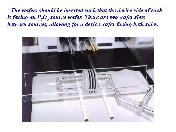
- The wafers should be inserted such that the device side of each is facing an P 2 O 5 source wafer. There are two wafer slots between sources, allowing for a device wafer facing both sides.

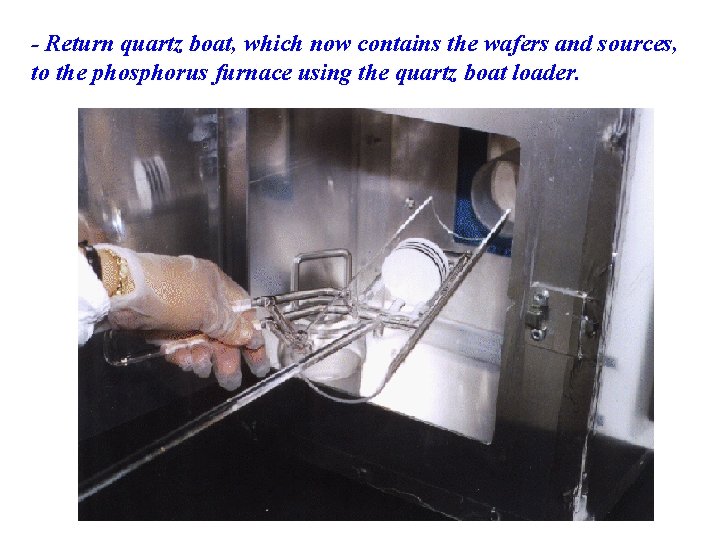
- Return quartz boat, which now contains the wafers and sources, to the phosphorus furnace using the quartz boat loader.

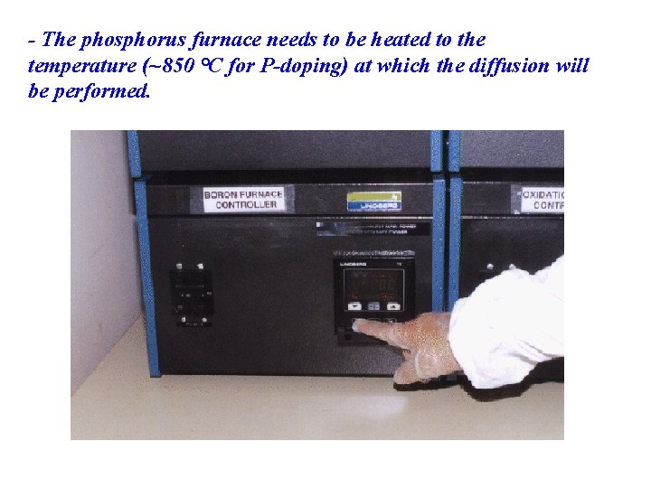
- The phosphorus furnace needs to be heated to the temperature (~850 °C for P-doping) at which the diffusion will be performed.

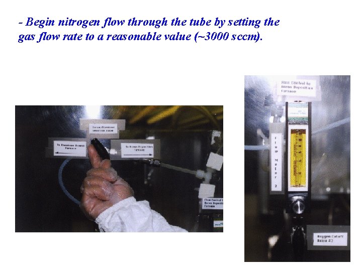
- Begin nitrogen flow through the tube by setting the gas flow rate to a reasonable value (~3000 sccm).

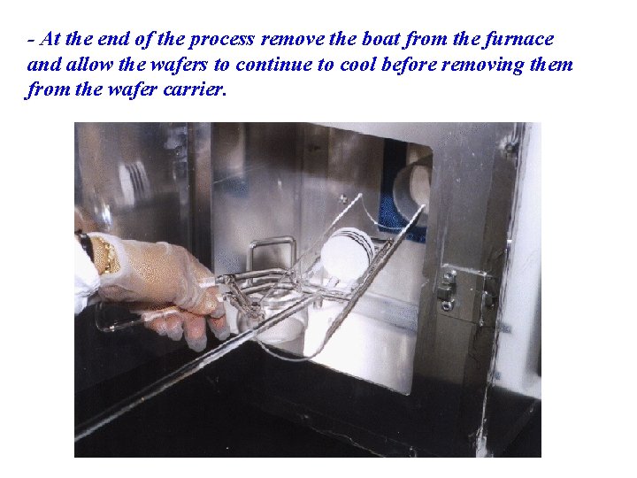
- At the end of the process remove the boat from the furnace and allow the wafers to continue to cool before removing them from the wafer carrier.

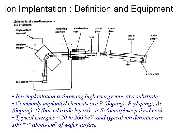
Ion Implantation : Definition and Equipment • Ion implantation is throwing high energy ions at a substrate. • Commonly implanted elements are B (doping), P (doping), As (doping), O (buried oxide layers), or Si (amorphise polysilicon). • Typical energies ~ 20 to 200 ke. V, and typical ion densities are 1011 to 16 atoms/cm 2 of wafer surface.

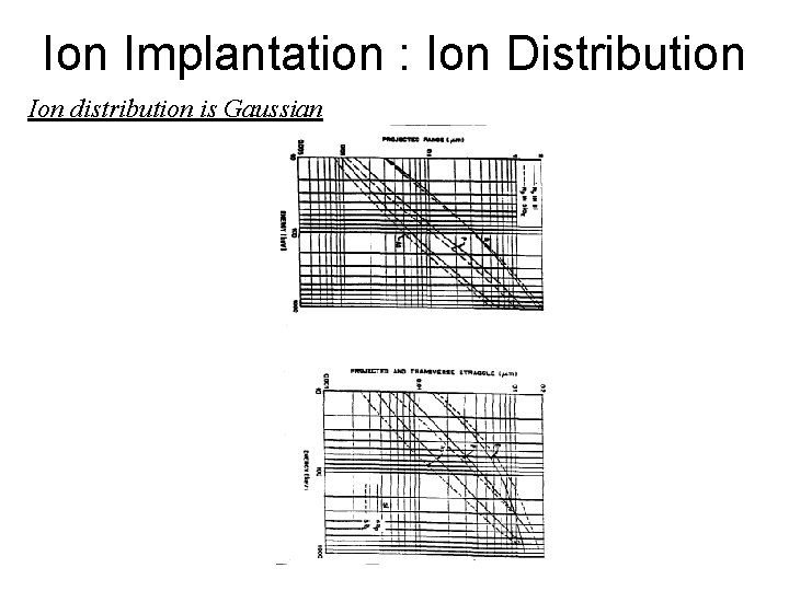
Ion Implantation : Ion Distribution Ion distribution is Gaussian

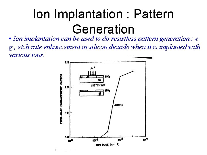
Ion Implantation : Pattern Generation • Ion implantation can be used to do resistless pattern generation : e. g. , etch rate enhancement in silicon dioxide when it is implanted with various ions.

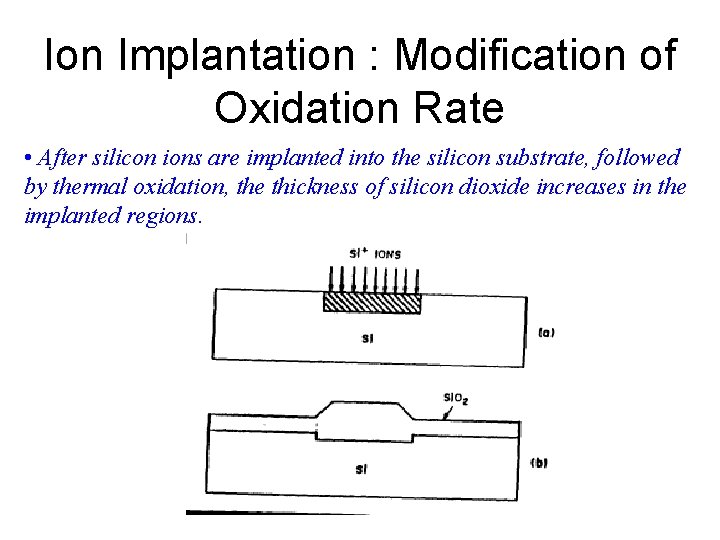
Ion Implantation : Modification of Oxidation Rate • After silicon ions are implanted into the silicon substrate, followed by thermal oxidation, the thickness of silicon dioxide increases in the implanted regions.