Differential Amplifier amplifies the difference between two input

Differential Amplifier • amplifies the difference between two input voltages • rejects the average or common mode value of the two voltages • v+, v-, vo are single ended • Diff-mode input: vid=v+ - v • Com-mode input: vic=(v+ + v- )/2 • vo =Avcvic + Avdvid • Avd: Diff voltage gain, Avc: CM voltage gain • Com-mode rejection ratio: Avd/Avc
 – vic range over which Avd remains")
Differential Amplifier • Input common-mode range (ICMR) – vic range over which Avd remains the same – Computed by requiring all MOST affected by vic to be in saturation • Output offset voltage Vos(out) – Voltage at vo when vid = 0 • Input offset voltage Vos – vid that is needed to make vo = 0 – When we say offset, default is input offset – Vos= Vos(out)/Avd, if Vos(out) is in linear range

Analysis of amplifiers • DC analysis – Find DC operating points, i. e. , quiescent point, or Q point – Finding the quiescent voltages VXXQ’s at various nodes – Finding IXXQ’s through various branches • Large signal static analysis – Plot of output versus input (transfer curve) – Large signal gain – Output and input swing limits • Small signal static and AC analysis – DC gain A 0, AC gain A(s) – Input resistance/impedance, output resistance/impedance • Small signal dynamic analysis – Bandwidth, overshoot, settling – Noise – Power supply rejection • Large signal dynamic analysis – Slew rate – Nonlinearity

Differential Input, single-ended output single stage Amplifier N-Channel vin+ vin-
2")
Large Signal Eq. in a N-channel Differential pair =0. 5 b 1(VGS 1 -VT)2 =(2 ID 1/b 1)0. 5 i. D 1=0, when i. D 2=ISS and VGS 2=VT+(2 ISS/b)0. 5
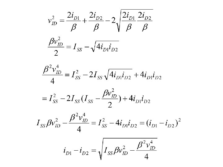

Solving for i. D 1 and i. D 2 i. D 1=i. D 2=ISS/2 VON 1=VON 2=(ISS/b)0. 5

N-Channel Input Pair Differential Amplifier

Voltage transfer curve

P-Channel Input Pair Differential Amplifier

Voltage transfer curve

INPUT COMMON MODE RANGE VG 1=VG 2=Vi. CM VSDSAT 1=VSDSAT 2 =VOD 1 VD 1=VD 3= VSS+VT 3+VOD 3 VG 1 min=VD 1 -|VT 1| =VSS+VOD 3+DVT VG 1 max=VDDVSD 5 SAT-|VT 1|-VOD

Output Range Vomin=Vss+Von 4 Vomax=Vicm –|VT 2| So what’s the vo range What’s for the N-ch circuit.

SMALL SIGNAL ANALYSIS AV
")
Common Mode Equivalent Circuit, with perfect match i. C 1=VIC/(1/gm 1 +2 rds 5) ro 1≈1/gm 3 i. C 1 ACM≈ 1/ 2 rds 5 gm 3

If not perfectly matched io=ai. IC a is a fraction go 1≈ gds 4 + gds 2/2 Av 5 ≈ gds 4 i. C 1 ACM ≈ agm 5 / 2 gds 4 CMRR=Av/ACM= gm 1/agm 5

SLEW RATE: the limit of the rate of change of the output voltage C’Ldvo/dt=i 4 -i 2 ISS Max |CLdvo/dt|=ISS Slew Rate = ISS/C’L ISS 0 Output swing: Vosw GB frequency: f. GB vo(t)=Voswsin(2 pf. GBt) Max dvo/dt =Vosw 2 pf. GB To avoid slewing: ISS > C’L Vosw 2 pf. GB

Parasitic Capacitances CT: common mode only CM: mirror cap = Cdg 1 + Cdb 1 + Cgs 3 + Cgs 4 + Cdb 3 COUT = output cap = Cbd 4 + Cbd 2 + Cgd 2 + CL

Cross CM disturbance After feed back, V+ very close to V-. Vcs 0. Vcs vic

how should the bulk be connected? Connect to source or connect n-well to VDD p-well to VSS

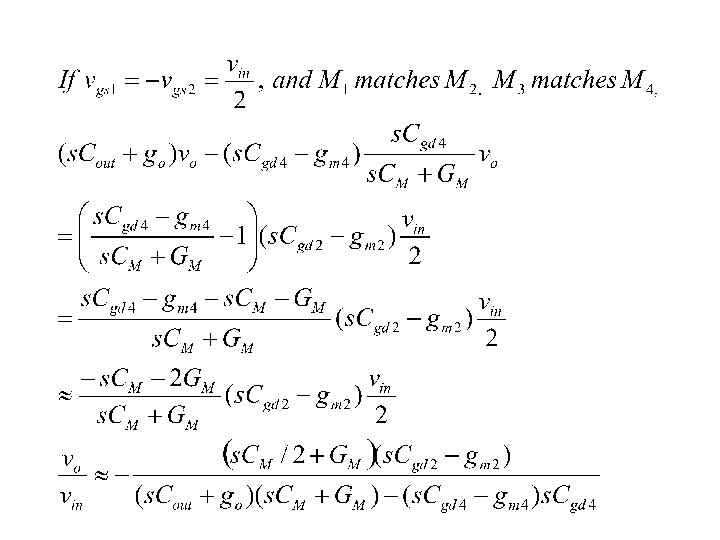
• Impedances – rout = rsd 2 || rds 4 = 1 / (gds 2 + gds 4) – r. M = 1/gm 3 || rds 1 ≈ 1/ gm 3 – Hence the output node is the high impedance node • When vi=0, slowest discharging node is output node with dominant pole p 1 = -1/(C’outrout), where C’out = Cout+ Cgd 4 • Approximate transfer function AV(s) = AV/(s/p 1─1)

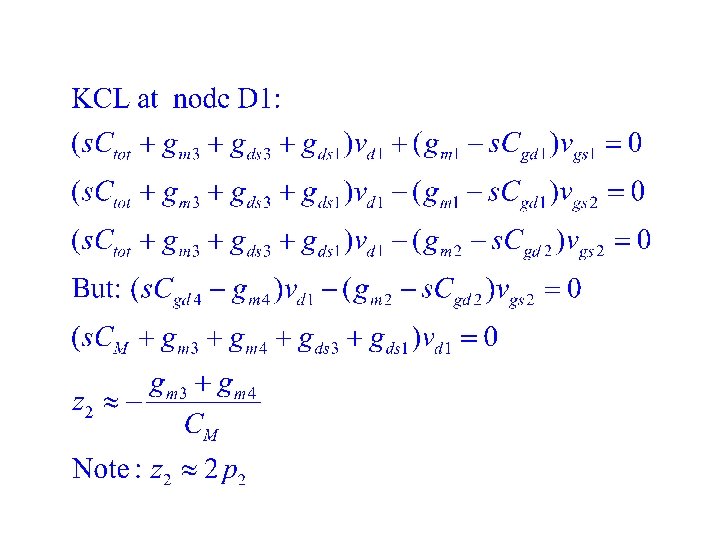
KCL at D 1: KCL at D 2:
 = gm 1 / (gds 2 +")
Gain bandwidth product • • Gain AV(0) = gm 1 / (gds 2 + gds 4) Bandwidth ≈ |p 1| ≈ (gds 2 + gds 4) / C’out GBW ≈ gm 1 / C’out gm 1 = {2*ID 1 m. Cox. W 1/L 1}½ – increase gm 1 increase GBW – increase W 1 increase GBW • But C’out has Cdb 2 and Cgd 2 W 1 – Once Cdb 2 and Cgd 2 become comparable to CL, increasing W 1 reduces GBW

Approximate poles and zeros VDD Second pole at D 1 M 4 r = 1/gm 3 Cgd 4 C = CM + M 3 (1+AV 4)Cgd 4 Vi+ M 1 Vb 2 M 5 VOUT Cgd 4 (1+AV 4)Cgd 4 CL AV 4 = gm 4/gds 4 Vi- p 2 = ─ gm 3 CM + (1+AV 4)Cgd 4
Cgd 4")
Approximate poles and zeros VDD M 3 M 4 Cgd 4 (1+AV 4)Cgd 4 Vi+ Apply miller effect M 1 Vb 2 M 5 VOUT Cgd 4 Vi- CL Set vin=0, write KCL at slowest Node to get p 1 Write KCL at other nodes for other poles Set vo=0, write KCL for zeros

VDD M 3 Unstable zero at Cgd 2 Enforce vo=0, float vin. M 4 ids 2, ids 4 = 0 VOUT CL Vi+ = - Vi- M 1 Vb 2 M 5 Vi- Cgd 2 dvi-/dt = gm 2 viz 1 = gm 2/Cgd 2

VDD For zero at D 1: M 3 For diff, Vi+ = - Vi- M 4 VOUT CL Vi+ M 1 Vb 2 M 5 Vi- Ctot = CM + Cgd 4
=AV(s/z 1 -1)(s/z 2 -1)/(s/p 1 -1)(s/p")
• A better approximation of TF: AV(s)=AV(s/z 1 -1)(s/z 2 -1)/(s/p 1 -1)(s/p 2 -1) • If p 1 is dominant, |p 1|<<|p 2|, |z 1|, |z 2|; AV(s)≈AV/(s/p 1 -1) • If p 1 is non-dominant, at low frequency, AV(s)≈AV /(s/p 1+s/p 2 -s/z 1 -s/z 2 -1) • 1/peq≈ 1/p 1+1/p 2 -1/z 1 -1/z 2 ≈ 1/p 1+1/p 2 -1/z 2 , since |z 1| >> |z 2|, |p 1|, |p 2|; ≈ 1/p 1, if AV 4 is not very large • In either case, BW ≈ p 1

frequency response AV All in abs val z 1 p 2 z 2 UGF w -90 -180 PM Small CL and small gm 3: gm 1/CL’ > gm 3/Cgs 3

frequency response AV All in abs val UGF w z 1 p 2 p 1 z 2 -90 PM -180 Large CL, gm 1/CL < gm 3/2 Cgs 3
 § GBW should be at least")
Observations • PM ≈ 90 – tan-1(UGF/z 1) § GBW should be at least 2~3 times lower than z 1 to ensure good phase margin at UGF § There is conflict between AV and PM • If z 2 not = p 2, UGF < AV*p 1 • Design approaches • make z 1 higher than UGF • make Cgd 2 small, gm 1 large • make z 2 close to p 2 better 1 st order approx. • make AV 4 small • make p 1 low large AV • make gds 2 and gds 4 small

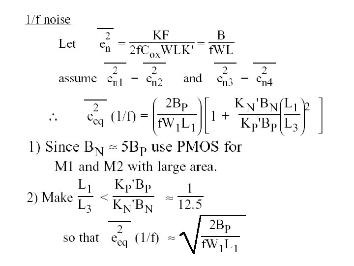
NOISE Model

Input equivalent noise source

• Total output noise current is found as, • Let • Then

How does this affect Av 4 and go?

One Quick Design Procedure • Select Iss based on SR – Iss = SR*CL *(1. 1~1. 2) • Select gm 1 based on GBW – gm 1 = GBW*CL’ • Get gm/ID for M 1, check if in proper range – If too high, increase ID ( => higher SR) – If too low, increase gm (=> high GBW) • • • Get ID/(W/L) from gm/ID ~ ID/(W/L) plot Get W/L from ID and ID/(W/L) Get W, by assuming L, for M 1 and M 2 Scale appropriately to get W, L for M 3, 4 Get size for M 5
- Slides: 39