Difference of optical microscope and electron microscope Electron


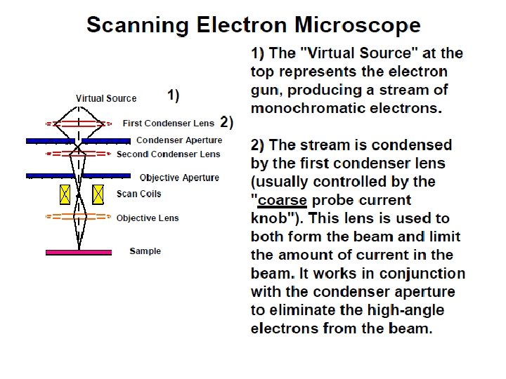
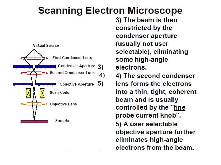
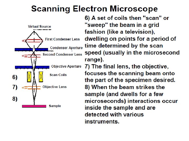
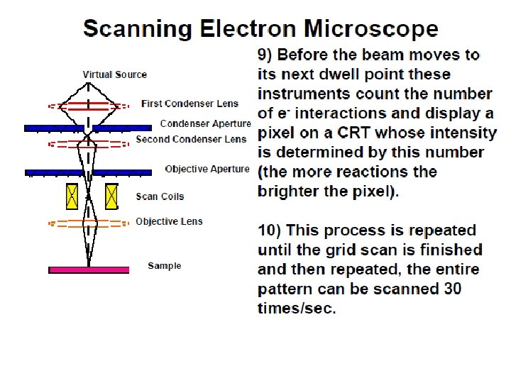
 2. Scanning Electron Microscope (SEM)")
 The scanning electron microscope (SEM) is a type of")
 Transmission electron microscopy (TEM) is a microscopy technique whereby")
")


 There are two types of electron guns: (i)")
 Thermionic guns, which are the most common type, apply thermal energy to a")

 Field emission guns, on the other hand, create a strong electrical field to")


 untreated bagasse fiber, (b) Na.")
 untreated fiber (500× magnification), (b) Na. OH")


. We")


 atom is ionized by removing a core electron, 2)")


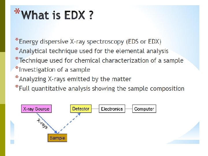
 p Energy Dispersive X-ray (EDX) is the method")


 pore")
 (b) SEM micrograph of (a) fracture surface of zirconia (x 500) and (b)")


- Slides: 113
Difference of optical microscope and electron microscope Electron microscopes have much microscopes greater resolving power than optical microscopes that use electromagnetic radiation and can obtain much higher magnifications of up to 2 million times, while the best optical microscopes are limited to magnifications of 2000 times.
Electron microscope An electron microscope is a type of microscope that uses a particle beam of electrons to illuminate a specimen and create a highly-magnified image.
Both electron and optical microscopes have resolution limitations, imposed by the wavelength of the radiation they use. wavelength radiation The greater resolution and magnification of the electron microscope is because the wavelength of an electron, is much smaller than that of a photon of visible light. * In physics, a photon is an elementary particle, the particle quantum of the electromagnetic field and the basic " unit " quantum field of light and all other forms of electromagnetic radiation. light radiation
Electromagnetic radiation is classified into several types according to the frequency of its wave; these types include (in order of increasing frequency and decreasing wavelength): radio waves, microwaves, infrared radiation, visible light, ultraviolet radiation, X-rays and gamma rays. X-rays
Electron Microscopes are scientific instruments that use a beam of highly energetic electrons to examine objects on a very fine scale. This examination can yield the following information: 1. 2. 3. 4. Topography Morphology Composition Crystallography Information
1. 1. Topography The surface features of an object or "how it looks", its texture; direct relation between these features and materials properties (hardness, reflectivity. . . etc. ) Fig. 4. (a) SEM morphological analysis of the Ti. Al. Si. N coating; (b) defects present in the film.
Brittle fracture of steel Mechanically alloyed Cu-Nb-Fe
2. Morphology The shape and size of the particles making up the object; direct relation between these structures and materials properties (ductility, strength, reactivity, etc. ) High resolution SEM image revealing nano-crystals covering up Fe oxide particle
Sn. O whiskers Iron oxide
3. Composition The elements and compounds that the object is composed of and the relative amounts of them; direct relationship between composition and materials properties (melting point, reactivity, hardness. . . etc. ) EDX analysis Micrograph Cr & Al mapping of sample neodymium (Nd)-doped yttrium aluminum garnet (YAG)
4. Crystallography information How the atoms are arranged in the object; direct relation between these arrangements and materials properties (conductivity, electrical properties, strength. . . etc. ) TEM image of oriented Single Crystal Gold Foil
Where did electron microscopes come from? p Electron Microscopes were developed due to the limitations of Light Microscopes which are limited by the physics of light to 1000 x or 2000 x magnification and a resolution of 0. 2 micrometers. q In the early 1930's this theoretical limit had been reached and there was a scientific desire to see the fine details of the interior structures of organic cells (nucleus, mitochondria. . . etc. ). q This required 10, 000 x plus magnification which was just not possible using Light Microscopes.
The basic steps involved in all EMs: 1. A stream of electrons is formed (by the electron source) electrons source and accelerated toward the specimen using a positive electrical potential. 2. This stream is confined and focused using metal apertures and magnetic lenses into a thin, focused, monochromatic beam. 3. This beam is focused onto the sample using a magnetic lens 4. Interactions occur inside the irradiated sample, affecting Interactions the electron beam 5. These interactions and effects are detected and transformed into an image
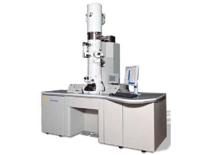
Types of Electron Microscopes 1. Transmission Electron Microscope (TEM) 2. Scanning Electron Microscope (SEM) 3. Reflection Electron Microscope (REM) 4. Scanning Transmission Electron Microscope (STEM)
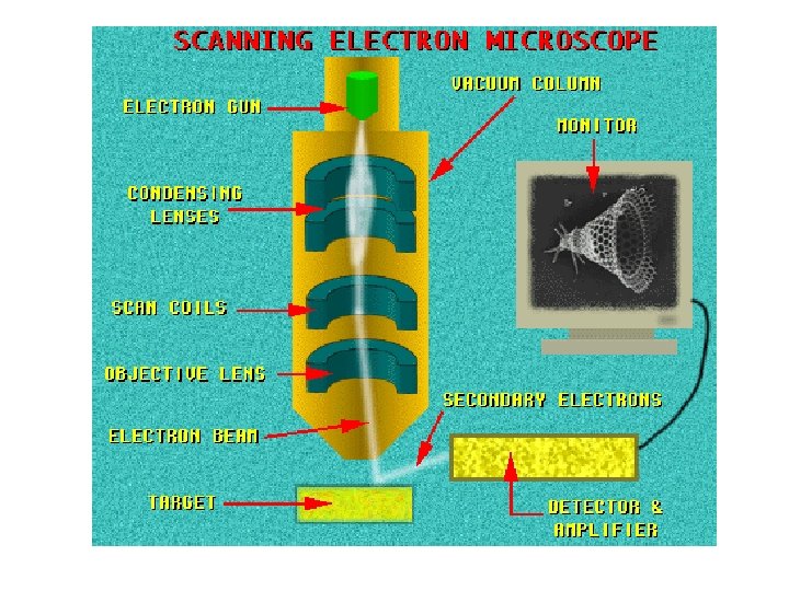
1. Scanning electron microscope (SEM) The scanning electron microscope (SEM) is a type of electron microscope that images the sample surface by scanning it with a high-energy beam of surface electrons in a raster scan pattern. The electrons interact with the atoms that make up the sample producing signals that contain information about the sample's surface topography, topography composition and other composition properties. Magnification in a SEM can be controlled over a range of up to 6 orders of magnitude from about x 25 to x 300, 000.
2. Transmission electron microscope (TEM) Transmission electron microscopy (TEM) is a microscopy technique whereby a beam of electrons is electrons transmitted through an ultra thin specimen, interacting specimen with the specimen as it passes through. An image is formed from the interaction of the electrons transmitted through the specimen; the image is magnified and focused onto an imaging device, such as a fluorescent screen, on a layer of photographic film, or to be detected screen by a sensor such as a CCD camera. - transmits a beam of electrons through a very thinly sliced specimen. TEM can magnify objects up to 1, 000 times.
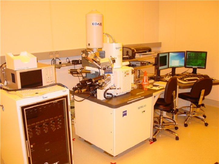
Scanning Electron Microscopes (SEM)
Model: Jeol JSM 6701 F Model: Keyence VE-9800
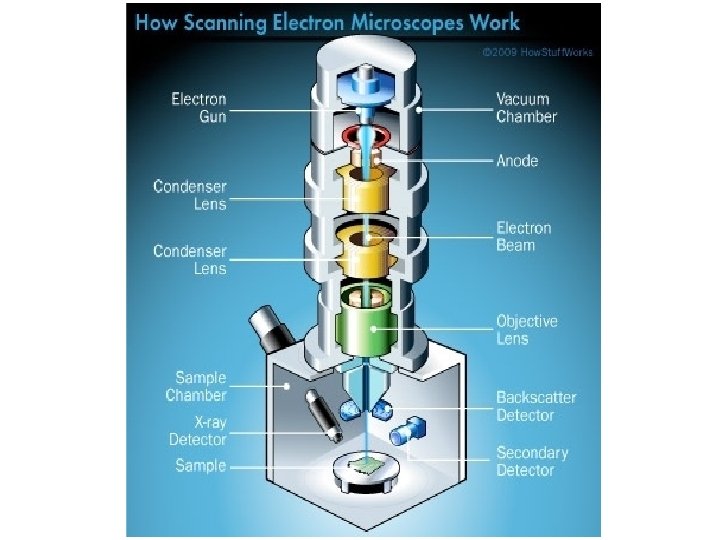
How does SEM work? The SEM is an instrument that produces a largely magnified image by using electrons instead of light to form an image. A beam of electrons is produced at the top of the microscope by an electron gun. The gun electron beam follows a vertical path through the microscope, which is held within a vacuum
The beam travels through electromagnetic fields and lenses, which focus the beam lenses down toward the sample. Once the beam hits the sample, electrons and X-rays are ejected from the sample.
Detectors collect these Xrays, backscattered electrons, and secondary electrons and convert them into a signal that is sent to a screen similar to a television screen. This produces the final image.
The Scanning Electron Microscope, or SEM, is an incredible tool for seeing the unseen worlds of microspace / nanospace.
Conventional light microscopes use a series of glass lenses to bend light waves and create a magnified image.
The SEM creates the magnified images by using electrons instead of light waves.
The SEM shows very detailed 3 -dimensional images at much higher magnifications than is possible with a light microscope.
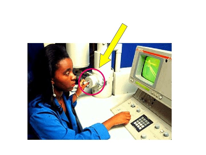
Samples have to be prepared carefully to withstand the vacuum inside the microscope.
Because the SEM illuminates them with electrons, samples have to be made to conduct electricity.
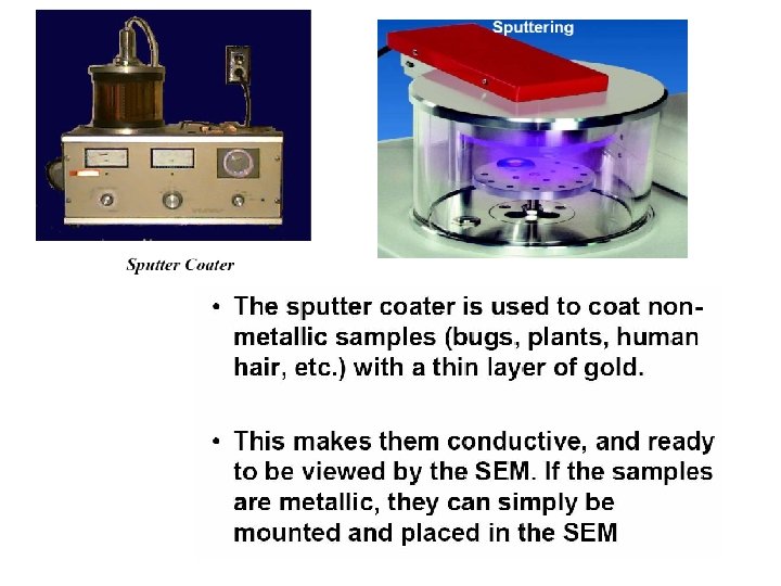
SEM samples are coated with a very thin layer of gold by a machine called a sputter coater.
Now the prepared specimen is ready.
The sample is placed inside the microscope's vacuum column through an air-tight door.
After the air is pumped out of the column, an electron gun [at the top] emits a beam of high energy electrons. This beam travels downward through a series of magnetic lenses designed to focus the electrons to a very fine spot.
Near the bottom, a set of scanning coils moves the focused beam back and forth across the specimen, row by row.
As the electron beam hits each spot on the sample, secondary electrons are knocked loose from its surface. A detector counts these electrons and sends the signals to an amplifier.
The final image is built up from the number of electrons emitted from each spot on the sample.
The Scanning Electron Microscope is revealing new levels of detail and complexity in the amazing world of micro-organisms and miniature structures.
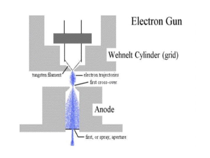
1. The electron source (Electron gun) There are two types of electron guns: (i) Thermionic guns (ii) Field emission guns
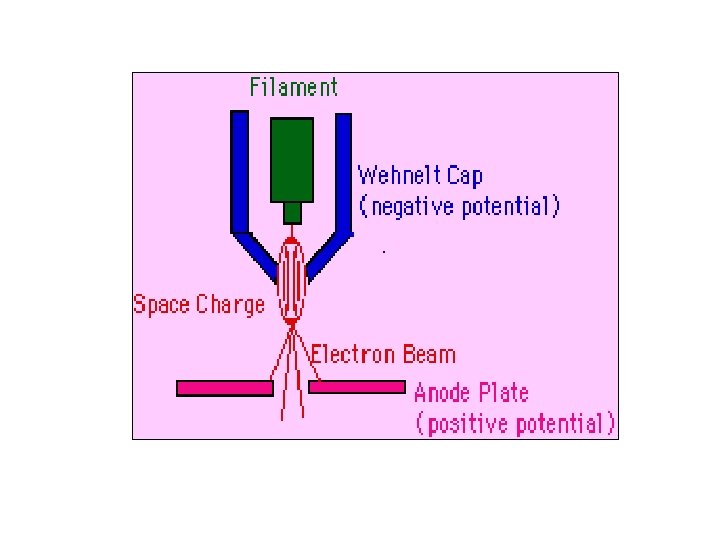
(i) Thermionic guns, which are the most common type, apply thermal energy to a energy filament (usually made of tungsten, which has a high melting point) to coax electrons away from the gun and toward the specimen under examination. * This filament is a loop of tungsten which functions as the cathode. A voltage is applied to the loop causing it to heat up.
The anode which is positive with respect to the filament forms powerful attractive forces for electrons. This causes electrons to accelerate toward the anode. Some accelerate right by the anode and down the column, to the sample. Other example of filament is Lanthanum Hexaboride (La. B 6) Filament
(ii) Field emission guns, on the other hand, create a strong electrical field to pull electrons away from the atoms they're associated with. Emitters are either of cold-cathode type, usually cold-cathode made of single crystal tungsten sharpened to a tip tungsten radius of about 100 nm, or of the Schottky type, in Schottky which emitters are made by coating a tungsten tip with a layer of zirconium oxide, which has the oxide unusual property of increasing in electrical conductivity at high temperature.
2. Condenser lenses Just like optical microscopes, SEMs use lenses to produce clear and detailed images. The lenses in these devices, however, work differently. For one thing, they aren't made of glass. Instead, the lenses are made of magnets lenses capable of bending the path of electrons. bending electrons Hence, the lenses can focus and control the electron beam, ensuring that the electrons end up precisely where they need to go.
3. Sample chamber The specimen must be kept extremely still for the microscope to produce clear images, so the sample chamber must be very sturdy and insulated from vibration. The sample chambers of an SEM do more than keep a specimen still. They also manipulate the specimen, placing it at manipulate different angles and moving it so that angles researchers don't have to constantly remount the object to take different images.
4. Detectors These devices detect the various ways that the electron beam interacts with the sample object. For instance, Everhart-Thornley detectors register secondary electrons, which are electrons dislodged from the outer surface of a specimen. These detectors are capable of producing the most detailed images of an object's surface. Other detectors, such as backscattered electron detectors and X-ray detectors, can tell researchers about the composition of a substance.
5. Vacuum chamber SEMs require a vacuum to operate. vacuum Without a vacuum, the electron beam generated by the electron gun would encounter constant interference from air particles in the atmosphere. interference Not only would these particles block the path of path the electron beam, they would also be knocked out of the air and onto the specimen, which would distort the surface of the specimen.
Reasons of Vacuum Condition p When a SEM is used, the column must always be at a vacuum. There are many reasons for this. 1. If the sample is in a gas filled environment, an electron beam cannot be generated or maintained because of a high instability in the beam. 2. Gases could react with the electron source, causing it to burn out or cause electrons in the beam to ionize, which produces random discharges and leads to instability in the beam. 3. The transmission of the beam through the electron optic column would also be hindered by the presence of other molecules.
4. The other molecules which could come from the sample or the microscope itself, could form compounds and condense on the sample. This would lower the contrast and obscure detail in the image. p A vacuum environment is also necessary in part of the sample preparation. One such example is the sputter coater. If the chamber isn’t at vacuum before the sample is coated, gas molecules would get in the way of the argon and gold. This could lead to uneven coating or no coating at all
Sample Preparation 1. Flat, polished surfaces provide grain structures and sizes information only after etched. 2. For any insulating ceramic sample, coating with a thin (10 nm) layer of gold, silver, copper or carbon to eliminate charging. The use of coating material will also enhanced the production of secondary electrons 3. Conductive path such as carbon or Al tape uses between sample and sample holder. 4. Samples should be clean from grease and dust particles.
Toilet paper Rice leaf
Cucumber leaf Mascara brush
Corrosion product on inside of Cu tubing Laser welded wire
Example of SEM micrograph of the cross-section of: (a) untreated bagasse fiber, (b) Na. OH treated fiber and (c) AA treated bagasse fiber (magnification 250×).
SEM micrographs of fiber surface of: (a) untreated fiber (500× magnification), (b) Na. OH treated fiber (500× magnification) and (c) AA treated fiber (300× magnification)
Schematic diagram of SEM Please see the given attachment. .
Advantages of using SEM • The SEM has a large depth of field, which allows a large amount of the sample to be in focus at one time. • The SEM also produces images of high resolution, which means that closely spaced features can be examined at a high magnification. • Preparation of the samples is relatively easy since most SEMs only require the sample to be conductive. • The combination of higher magnification, larger depth of focus, greater resolution, and ease of sample observation makes the SEM one of the most heavily used instruments in research areas today.
Interaction between electron beam and specimens § Specimen interaction is what makes Electron Microscopy possible. § The energetic electrons in the microscope strike the sample and various reactions can occur as shown in the following slide.
Electron / Specimen Interactions When the electron beam strikes the sample, both photon and electron signals are emitted.
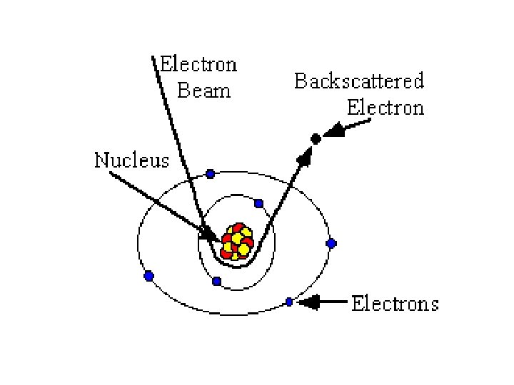
Difference of Backscattered and Secondary Electrons The incident electrons cause electrons to be emitted from the sample due to elastic and inelastic scattering events within the scattering sample’s surface and near-surface material. High-energy electrons that are ejected by an electrons elastic collision of an incident electron, collision typically with a sample atom’s nucleus, are nucleus referred to as backscattered electrons. The electrons energy of backscattered electrons will be comparable to that of the incident electrons. comparable
Difference of Backscattered and Secondary Electrons Emitted lower-energy electrons resulting electrons from inelastic scattering are called scattering secondary electrons. Secondary electrons can be formed by collisions with the nucleus where substantial energy loss occurs or by loss the ejection of loosely bound electrons from the sample atoms.
Objective lens • The lens that focuses the beam of electrons towards the sample is in the center of the picture. The parts off to the right of the sample are different detectors. One is for detecting the secondary electrons and the other is for detecting the backscattered electrons. The operator has the power to choose and switch detectors for use on each sample.
Backscattered Electrons Backscattered electrons are produced by the elastic interactions between the sample and interactions the incident electron beam. These highenergy electrons can escape from much deeper than secondary electrons, so surface topography is not as accurately resolved. Formation q Caused by an incident electron colliding with an atom in the specimen which is nearly normal to the incident's path.
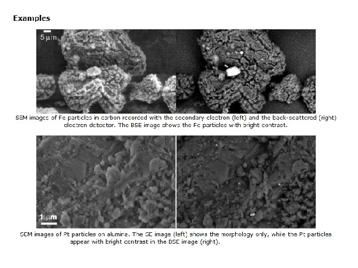
Utilization The production of backscattered electrons varies directly with the specimen's atomic number. directly number This differing production rates causes higher atomic number elements to appear brighter than lower brighter atomic number elements which results in image contrast as a function of composition. contrast composition This interaction is utilized to differentiate parts of parts the specimen that have different average atomic number An example is shown in the SEM output section, specifically the mechanically alloyed specimen micrograph.
The backscattered electron detector produces an image that is useful when determining the make-up of the sample. Each element in the sample appears as a different shade, from almost white to black. This is an image of an aluminum copper alloy formed using backscattered electron imaging. The light area is mostly copper and the dark area is mostly aluminum Atomic No. Cu = 63. 55, Al = 27
Figure 1: Electronic transitions in a calcium atom. Remember, when electrons are jumping down, one of the electrons in the outer shell is missing!
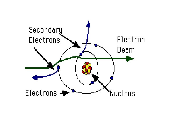
Secondary Electrons Secondary electrons are produced by the inelastic interactions between interactions the sample’s electron and the incident electron beam results in the emission of low-energy electrons from near the sample's surface.
Secondary Electrons. Source q Caused by an incident electron passing "near" an atom in the specimen, near enough to impart some of its energy to a lower energy electron (usually in the K-shell). q This causes a slight energy loss and path change in the incident electron and the ionization of the electron in the specimen atom. q This ionized electron then leaves the atom with a very small kinetic energy (5 e. V) and is then termed a "secondary electron". q Each incident electron can produce several secondary electrons.
Utilization q Production of secondary electrons is very topography related. Provides High-resolution Imaging Of Fine Surface Morphology q Due to their low energy, 5 e. V, only secondaries that are very near the surface (<10 nm) can exit the sample and be examined. q Any changes in topography in the sample that are larger than this sampling depth will change the yield of secondaries due to collection efficiencies.
The topography of surface features influences the number of electrons that reach the secondary electron detector from any point on the scanned surface. This local variation in electron intensity creates the image contrast that reveals the surface morphology. Collection of these electrons is aided by using a "collector" in conjunction with the secondary electron detector.
Using the secondary electron detector produces a clear and focused topographical image of the sample. This is an image of the broken surface of a piece of metal, formed using secondary electron imaging.
The image illustrates 2 different scanning modes of a scanning electron microscope (SEM). We can see light spots surrounded by darker areas. The light spots correspond to the zirconium aggregates in an aluminium matrix. This is obtained using the detection of backscattered electrons We can see the relief of the sample. This is obtained using the detection of secondary electrons
Cathodoluminescence The emission of ultraviolet, ultraviolet visible, or visible infrared light stimulated by electron light bombardment is known as bombardment cathodoluminescence (CL) and it is (CL) frequently observed when examining minerals or semiconductor using an semiconductor electron microscope.
Formation Cathodoluminescence occurs because the impingement of a high energy electron beam impingement beam onto a semiconductor will result in the promotion of electrons from the valence band into the band conduction band, leaving behind a hole. band hole When an electron and a hole recombine, it is recombine possible for a photon to be emitted. The energy photon emitted (color) of the photon, and the probability that a photon will be emitted, depends on the material, its purity, and its defect state.
Utilization The primary advantages to the electron microscope based technique of CL is the ability to resolve features down to 10 -20 nm, the ability to measure an entire nm spectrum at each point if the photomultiplier tube is spectrum replaced with a CCD camera. CL can provide images clearly showing crystal growth chemistry, alteration chemistry intercrystalline boundaries, and boundaries alteration due to weathering or leaching CL spectra can be used to differentiate some trace differentiate element abundances and differentiate phases based abundances phases on spectral shape
Applications in Mineral CL emissions can provide general information on the trace elements contained in minerals or the production minerals of mechanically induced defects in the crystals. defects crystals Investigations of cementation and diagenesis processes in sedimentary rocks Provenance of clastic material in sedimentary and meta-sedimentary rocks Details of internal structures of fossils Growth/dissolution features in igneous and metamorphic minerals Deformation mechanisms in metamorphic rocks.
Sandstone sample from unknown formation. Mostly ankerite-filled almost macrofractures. A few spots (such as in the light-blue grain at the bottom) are filled with quartz, mostly macros are calcite filled. Secondary electron image of the same field of view as the above CL image
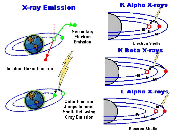
X-ray When the incident beam bounces through the sample creating secondary electrons, it leaves thousands of the sample atoms with holes in the electron shells where the secondary electrons used to be. If these "holes" are in inner shells, the atoms are shells not in a stable state. To stabilize the atoms, stabilize electrons from outer shells will drop into the inner shells drop shells, however, because the outer shells are at a shells higher energy state, to do this the atom must lose state some energy. It does this in the form of X-rays. energy X-rays
Utilization q X-rays emitted from the atom will have a characteristic energy which is unique to the element from which it originated. q These signals are collected and sorted according to energy of bulk specimens limiting the point-to-point comparisons available.
Auger Electrons Source Caused by the de-energization of the specimen de-energization atom after a secondary electron is produced. electron Since a lower (usually K-shell) electron was emitted from the atom during the secondary electron process an inner (lower energy) shell now has a vacancy. A higher energy electron from the same atom can "falls" to a lower energy, filling the vacancy. This creates and energy surplus in the atom which can be corrected by emitting an outer (lower energy) electron; an Auger Electron
There are 3 steps: 1) atom is ionized by removing a core electron, 2) upper level electron falls to lower level, 3) third electron (Auger electron) is excited by the energy given off in step 2 and detected The atom is left with two vacancies.
Utilization q Auger Electrons have a characteristic energy, unique to each element from which it was emitted from. q These electrons are collected and sorted according to energy to give compositional information about the specimen. q Since Auger Electrons have relatively low energy they are only emitted from the bulk specimen
This technique is particularly useful for determining the elemental composition of the surface because Auger electrons have a limited escape depth. A key capability of the field emission Auger electron spectroscopy (FE-AES) is its ability to focus the electron beam to a small spot, with resolutions similar to an electron microscope. (a) SEM and (b&c) SAM images of a surface defect in Cu(In, Ga)Se. S. SAM analysis shows the defect to be an In-rich region (b), indicating that the likely origin was an "In-spit" during precursor deposition that was subsequently selenized during downstream processing (c).
SEM + Microanalysis (EDX / EDS) p Energy Dispersive X-ray (EDX) is the method of determining the chemical composition of microscopic area of a solid sample p In tandem with the SEM, it is possible to prepare a photographic record of the materials and textural characteristics of the regions analyzed by EDX.
An example spectrum for phosphorous with fluorine. The element peaks for analysis have been marked in red. The x-axis of the spectrum is the x-ray energy scale, along which x-rays collected from various elements are registered, and which in turn form a series of peaks along the x-axis where each peak corresponds to a particular element.
• The principle is that the electron beam of the SEM causes atoms in the field of the view to emit X-rays the energy of which is characteristic X-rays of the emitting element • By this method it is possible to analyze a particular point on a surface as small as a few microns across. This facility can be used fully quantitatively for a wide range of elements on elements a multitude of samples, such as polished surfaces, fracture surfaces, powders and surface films.
If one spot only is analyzed, quantification of the relative proportions of elements under that spot is possible, which is known as point analysis. If however a line of pixels is analyzed, a linetraverse analysis can be performed which can highlight changing proportions of elements with elements distance along the line. This is known as line scanning. Finally, each pixel in an image can also be analyzed, which illustrates the distribution of a chosen element across the image. This is known element as dot-mapping of the elements,
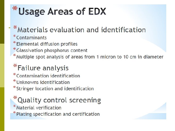
SEM-EDX Applications 1. Elemental profiling across physical and mineralogical boundaries 2. Assessment of the distribution of minor elements with respect to component phases in any given material 3. Detection of light elements- boron, carbon, oxygen and fluorine 4. Quantitative analyses of solids including individual mineral grains and interstitial glasses allowing improved understanding of chemical-related phenomena such as thermal expansion and melting points
5. The ability to quote less than figures for those elements not detected in a particular sample 6. Quantitative analyses of unpolished materials such as powders, fractures surfaces and surface films 7. Mapping element distributions within a given sample 8. The distribution of carbon, nitrogen and oxygen in industrial ceramics 9. Analysis and characterization of inorganic specks within white wares, refractories, enamels, glasses, plastics and other materials 10. Microanalysis of filler materials used in plastics, paints and other manufactured materials
C B
Micrograph SEM ceramics grain Grain boundary 5μm SEM micrograph of HA (x 3000) pore 5μm SEM micrograph of Al 2 O 3 (x 5000)
(a) (b) SEM micrograph of (a) fracture surface of zirconia (x 500) and (b) polish and etched structure of zirconia (x 20000)
Micrograph SEM polymer
Fig. 1. SEM micrographs showing mechanical milling evolution of copper. In the early stage of milling powders are flat and have a rather wide size distribution. Smaller uniform particle size was observed for longer milling time. (a) 4 h milled, (b) 6 h milled, (c) 12 h milled and (d) 15 h milled.
Electrons in Transmission & Scanning Electron Microscopy In TEM as well as SEM the sample is bombarded by a beam of electrons, so called primary electrons that originate from an electron gun. The principles of image formation, however, differ: TEM SEM