
DI Water Reduction in Rinse Processes Contributions by
DI Water Reduction in Rinse Processes Contributions by: Thomas W. Peterson, University of Arizona Andy Hebda, University of Arizona Thomas Roche, Motorola Corp. Eric Hansen, Santa Clara Plastics 1999 Arizona Board of Regents for The University of Arizona 1 NSF/SRC Engineering Research Center for Environmentally Benign Semiconductor Manufacturing
Overview • DI water use during rinsing: – ~ 103 gallons/wafer ==> ~107 - 108 gallons/year (SEMATECH) • Minimal recycle and reuse across the industry • Primary objective: CLEAN WAFERS 2 NSF/SRC Engineering Research Center for Environmentally Benign Semiconductor Manufacturing
Indicators of “Clean Wafers” • ON-LINE – Resistivity in the Rinse Tank • OFF-LINE – Particle Counts on Wafer Surface – Elemental Analysis of Wafer Surface – Device Characteristics Testing 3 NSF/SRC Engineering Research Center for Environmentally Benign Semiconductor Manufacturing
Terminology • Resistivity – Primary measurement of ionic concentration of rinse water. The higher the ion concentration, the lower the resistivity. – [=] MW - cm • Conductivity – The inverse of resistivity. For dilute solutions, conductivity is proportional to ionic concentration – [=] 1/ (MW - cm) 4 NSF/SRC Engineering Research Center for Environmentally Benign Semiconductor Manufacturing
Terminology (cont’d) • Integrated Conductivity – The conductivity in the rinse water integrated over the time period required to “recover” from the chemical burden introduced to the system by the wafers • Carryover – Amount (moles or grams) of chemical “carried over” with the wafers and the boat from » chemistry tank to first rinse tank » first rinse tank to second rinse tank 5 NSF/SRC Engineering Research Center for Environmentally Benign Semiconductor Manufacturing
“Typical” DI Water Resistivity (MW - cm) • Clean water, high flow conditions (greater than 11 gpm): 17 - 18+ • Clean water, low flow conditions: 8 -17 or lower • Rinse bath containing wafers, immediately following chemistry: <<0. 01 (mdl for monitor) 6 NSF/SRC Engineering Research Center for Environmentally Benign Semiconductor Manufacturing
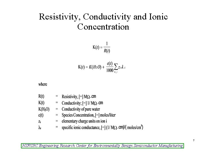
Resistivity, Conductivity and Ionic Concentration 7 NSF/SRC Engineering Research Center for Environmentally Benign Semiconductor Manufacturing
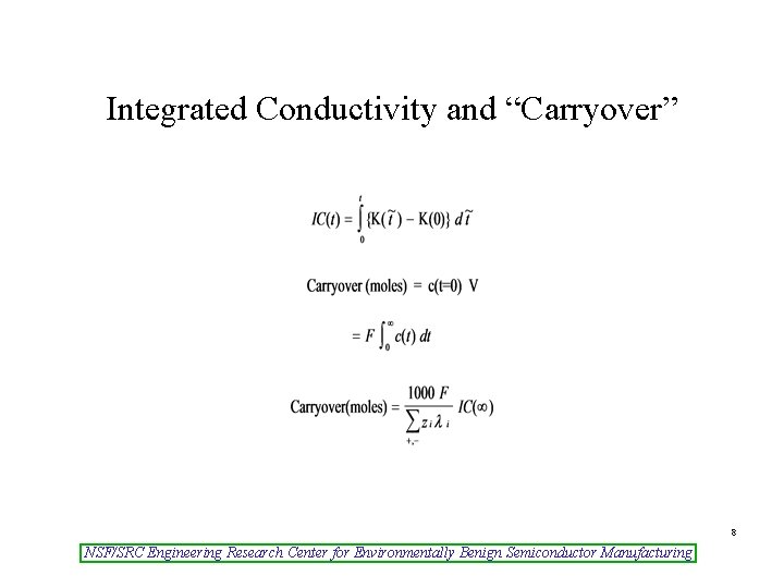
Integrated Conductivity and “Carryover” 8 NSF/SRC Engineering Research Center for Environmentally Benign Semiconductor Manufacturing
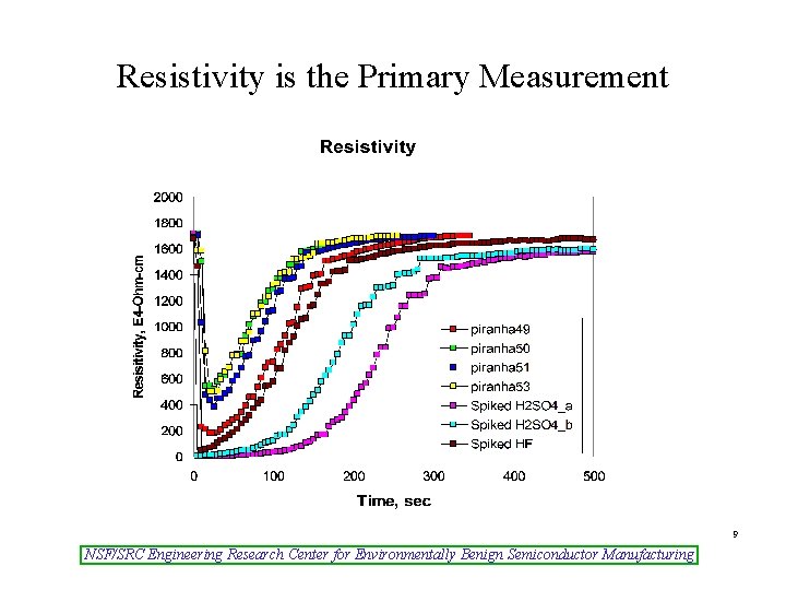
Resistivity is the Primary Measurement 9 NSF/SRC Engineering Research Center for Environmentally Benign Semiconductor Manufacturing
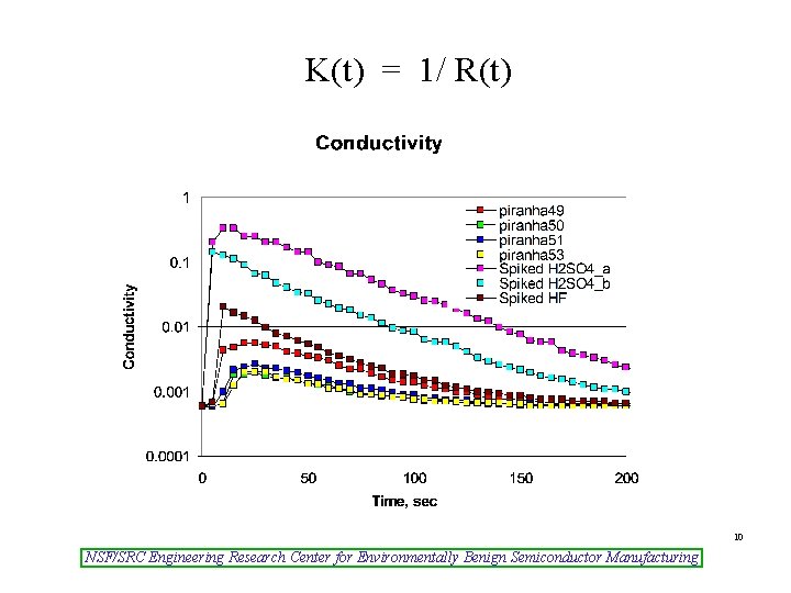
K(t) = 1/ R(t) 10 NSF/SRC Engineering Research Center for Environmentally Benign Semiconductor Manufacturing
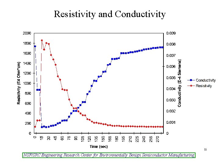
Resistivity and Conductivity 11 NSF/SRC Engineering Research Center for Environmentally Benign Semiconductor Manufacturing
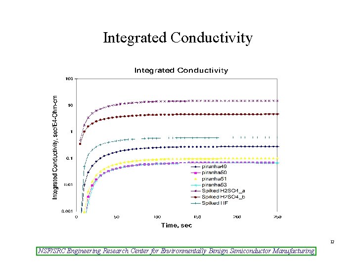
Integrated Conductivity 12 NSF/SRC Engineering Research Center for Environmentally Benign Semiconductor Manufacturing
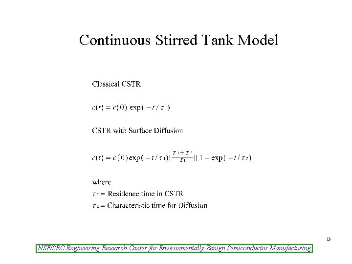
Continuous Stirred Tank Model 13 NSF/SRC Engineering Research Center for Environmentally Benign Semiconductor Manufacturing
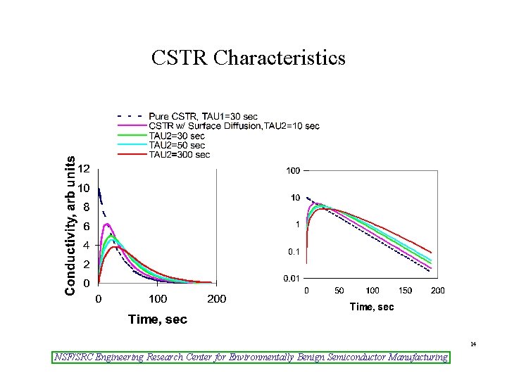
CSTR Characteristics 14 NSF/SRC Engineering Research Center for Environmentally Benign Semiconductor Manufacturing
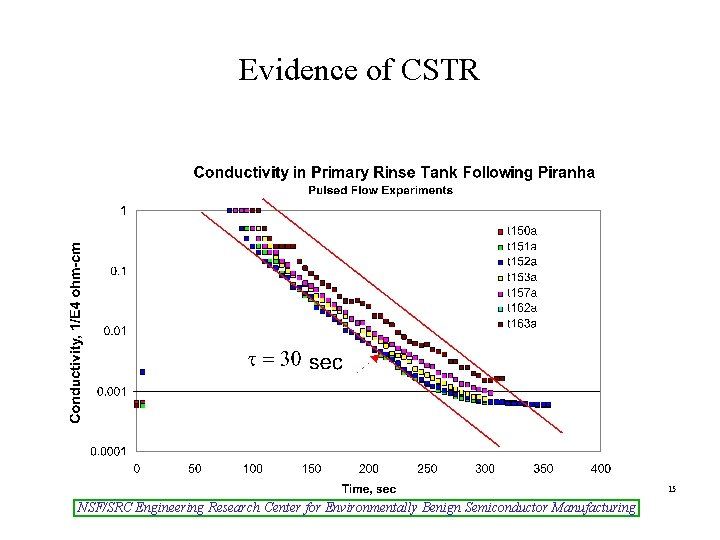
Evidence of CSTR 15 NSF/SRC Engineering Research Center for Environmentally Benign Semiconductor Manufacturing
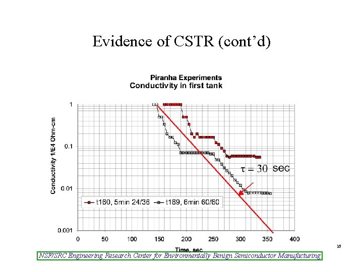
Evidence of CSTR (cont’d) 16 NSF/SRC Engineering Research Center for Environmentally Benign Semiconductor Manufacturing
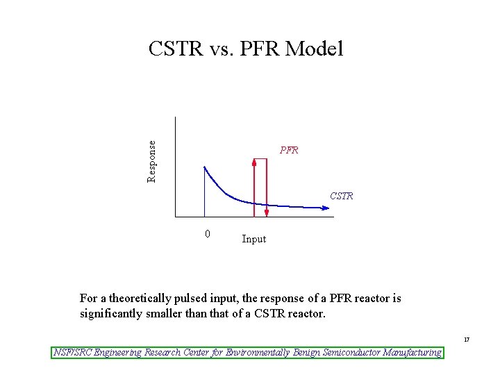
Response CSTR vs. PFR Model PFR CSTR 0 Input For a theoretically pulsed input, the response of a PFR reactor is significantly smaller than that of a CSTR reactor. 17 NSF/SRC Engineering Research Center for Environmentally Benign Semiconductor Manufacturing
Hypothesis: Wafers can be adequately “cleaned and rinsed” with less water • Select the methods of reduction • Establish “base-line” water requirements for current processes • Alter water usage in rinse bath by various means • Examine “Indicators” of wafer cleanliness 18 NSF/SRC Engineering Research Center for Environmentally Benign Semiconductor Manufacturing
Methods for DI Reduction • Pulsed rinse baths – HF chemistry – Piranha (H 2 SO 4/H 2 O 2) chemistry • Decrease in bath volume 19 NSF/SRC Engineering Research Center for Environmentally Benign Semiconductor Manufacturing
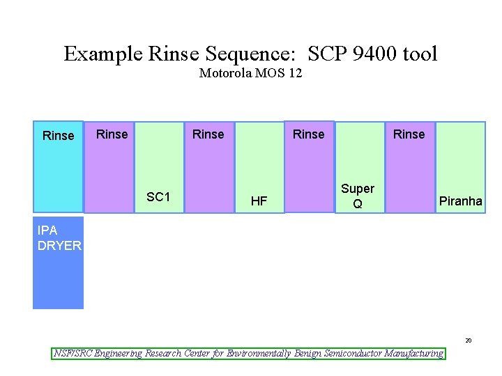
Example Rinse Sequence: SCP 9400 tool Motorola MOS 12 Rinse SC 1 Rinse HF Rinse Super Q Piranha IPA DRYER 20 NSF/SRC Engineering Research Center for Environmentally Benign Semiconductor Manufacturing
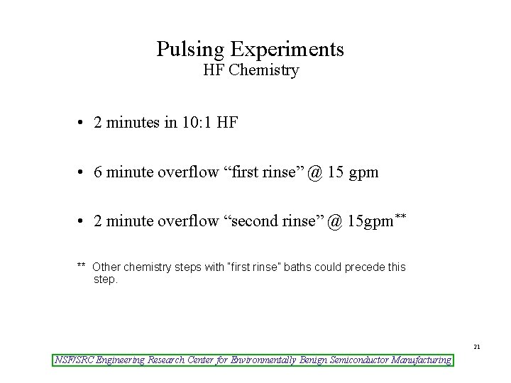
Pulsing Experiments HF Chemistry • 2 minutes in 10: 1 HF • 6 minute overflow “first rinse” @ 15 gpm • 2 minute overflow “second rinse” @ 15 gpm** ** Other chemistry steps with “first rinse” baths could precede this step. 21 NSF/SRC Engineering Research Center for Environmentally Benign Semiconductor Manufacturing
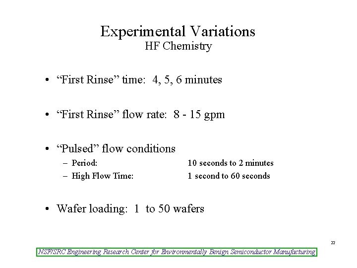
Experimental Variations HF Chemistry • “First Rinse” time: 4, 5, 6 minutes • “First Rinse” flow rate: 8 - 15 gpm • “Pulsed” flow conditions – Period: – High Flow Time: 10 seconds to 2 minutes 1 second to 60 seconds • Wafer loading: 1 to 50 wafers 22 NSF/SRC Engineering Research Center for Environmentally Benign Semiconductor Manufacturing
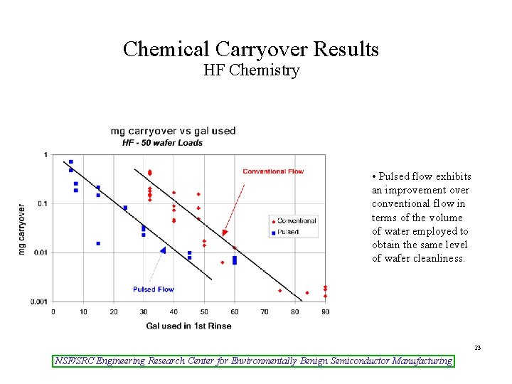
Chemical Carryover Results HF Chemistry • Pulsed flow exhibits an improvement over conventional flow in terms of the volume of water employed to obtain the same level of wafer cleanliness. 23 NSF/SRC Engineering Research Center for Environmentally Benign Semiconductor Manufacturing
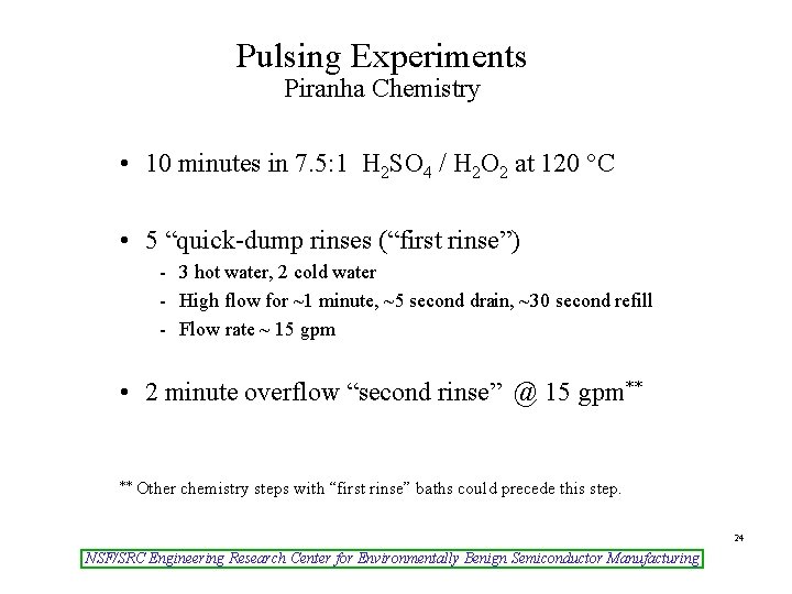
Pulsing Experiments Piranha Chemistry • 10 minutes in 7. 5: 1 H 2 SO 4 / H 2 O 2 at 120 °C • 5 “quick-dump rinses (“first rinse”) - 3 hot water, 2 cold water - High flow for ~1 minute, ~5 second drain, ~30 second refill - Flow rate ~ 15 gpm • 2 minute overflow “second rinse” @ 15 gpm** ** Other chemistry steps with “first rinse” baths could precede this step. 24 NSF/SRC Engineering Research Center for Environmentally Benign Semiconductor Manufacturing
Experimental Variations Piranha Chemistry • • • ~ 50 experiments conducted “First Rinse” utilized both quick dump and overflow modes “First Rinse” time 3 - 9 minutes “First Rinse” flow rate 8 - 15 gpm “Pulsed” Flow conditions – period: – high flow time: 10 seconds to 4 minutes 2 seconds to 2 minutes • Hot and Cold Rinses • “Agitation” (using robot arm) 25 NSF/SRC Engineering Research Center for Environmentally Benign Semiconductor Manufacturing
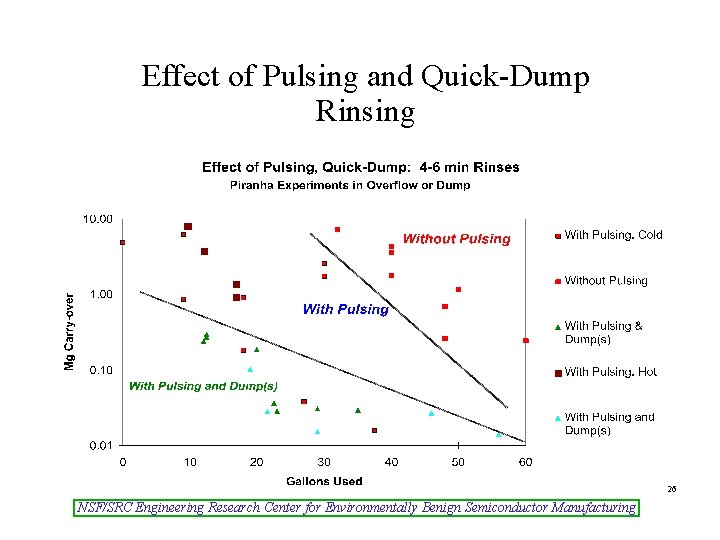
Effect of Pulsing and Quick-Dump Rinsing 26 NSF/SRC Engineering Research Center for Environmentally Benign Semiconductor Manufacturing
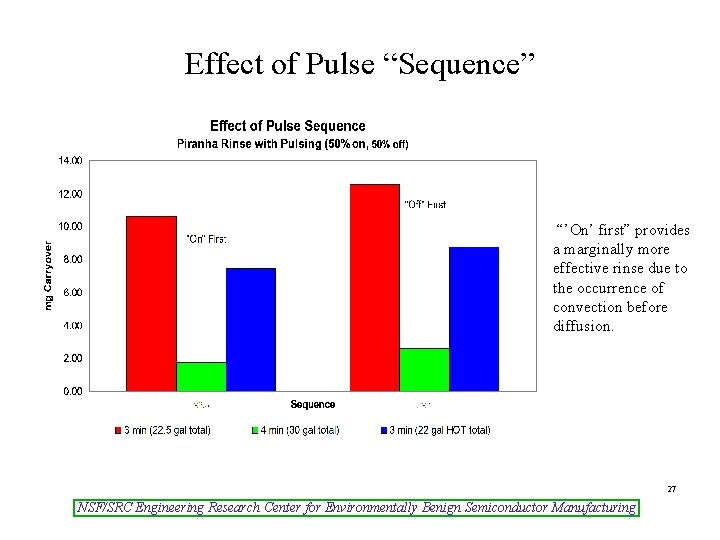
Effect of Pulse “Sequence” “’On’ first” provides a marginally more effective rinse due to the occurrence of convection before diffusion. 27 NSF/SRC Engineering Research Center for Environmentally Benign Semiconductor Manufacturing
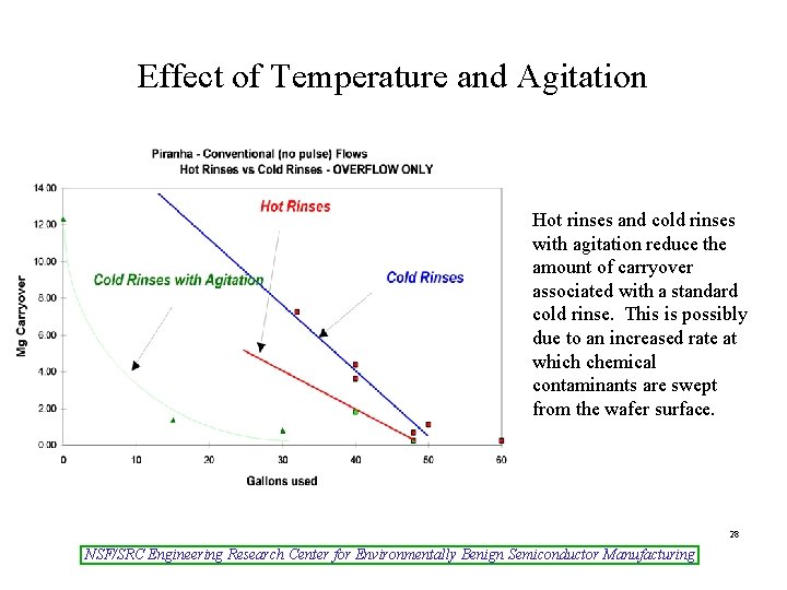
Effect of Temperature and Agitation Hot rinses and cold rinses with agitation reduce the amount of carryover associated with a standard cold rinse. This is possibly due to an increased rate at which chemical contaminants are swept from the wafer surface. 28 NSF/SRC Engineering Research Center for Environmentally Benign Semiconductor Manufacturing
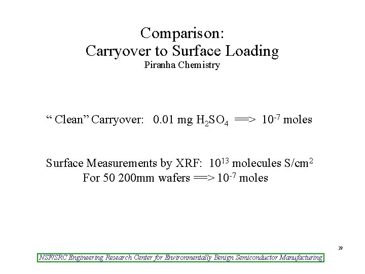
Comparison: Carryover to Surface Loading Piranha Chemistry “ Clean” Carryover: 0. 01 mg H 2 SO 4 ==> 10 -7 moles Surface Measurements by XRF: 1013 molecules S/cm 2 For 50 200 mm wafers ==> 10 -7 moles 29 NSF/SRC Engineering Research Center for Environmentally Benign Semiconductor Manufacturing
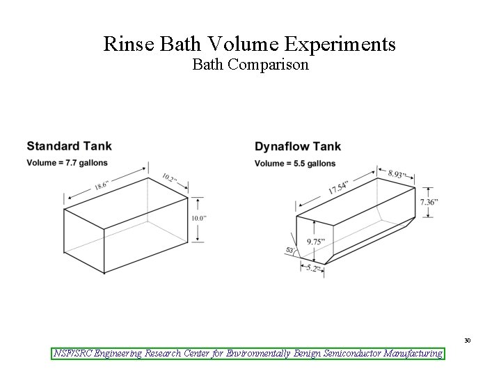
Rinse Bath Volume Experiments Bath Comparison 30 NSF/SRC Engineering Research Center for Environmentally Benign Semiconductor Manufacturing
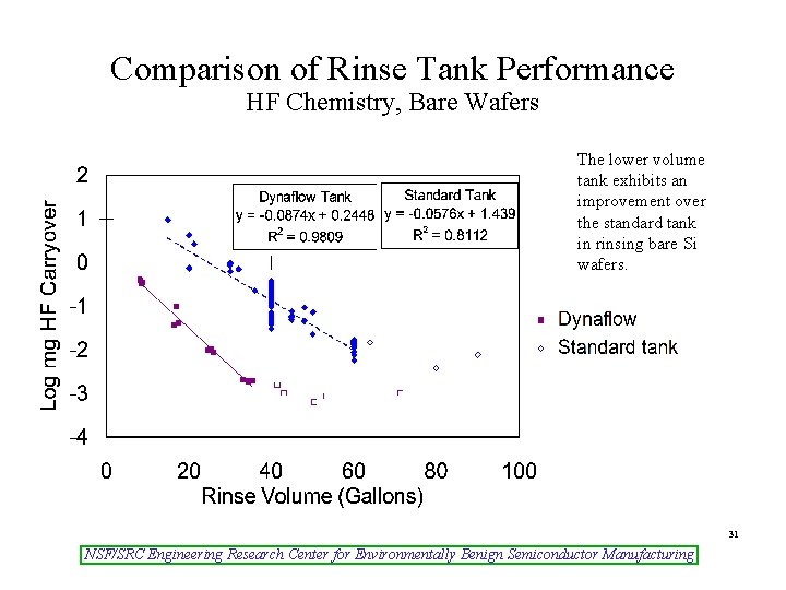
Comparison of Rinse Tank Performance HF Chemistry, Bare Wafers The lower volume tank exhibits an improvement over the standard tank in rinsing bare Si wafers. 31 NSF/SRC Engineering Research Center for Environmentally Benign Semiconductor Manufacturing
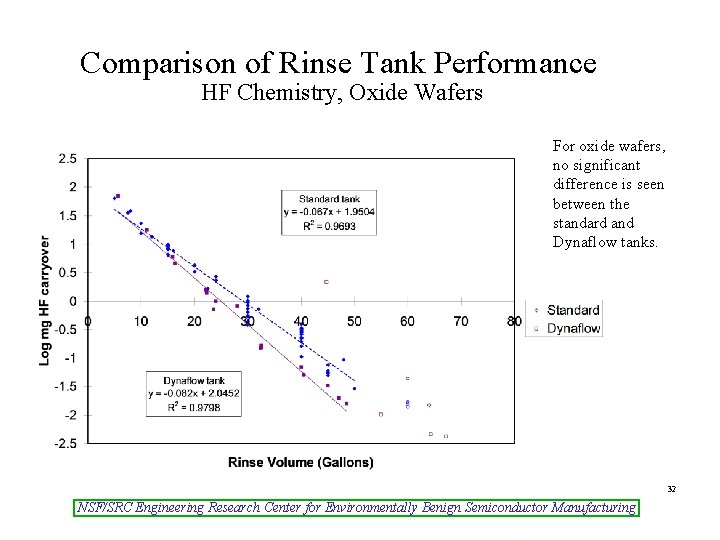
Comparison of Rinse Tank Performance HF Chemistry, Oxide Wafers For oxide wafers, no significant difference is seen between the standard and Dynaflow tanks. 32 NSF/SRC Engineering Research Center for Environmentally Benign Semiconductor Manufacturing
Summary • Under certain conditions, pulsing has a pronounced effect on rinse efficiency. • Combining pulsing sparingly with quick-dumps (in those processes which allow for quick-dumps) can further increase rinse efficiency. • A substantial portion of the time during rinsing is spent “cleaning up the water” rather than cleaning up the wafer surface. • Moving the characteristic operating conditions of the rinse tank closer to Plug flow conditions can potentially reduce water usage over that required for CSTR conditions. • A new rinse bath shape using less water volume can decrease water usage while achieving an effective rinse for bare silicon wafers. 33 NSF/SRC Engineering Research Center for Environmentally Benign Semiconductor Manufacturing
- Slides: 33