Device Interface Board for Wireless LAN Testing Faculty
Device Interface Board for Wireless LAN Testing Faculty Advisor Dr. Weber Team May 06 -15 Team Members Matthew Dahms – EE Justine Skibbe – EE Joseph Chongo – EE Client ECp. E Department February 9, 2006
Presentation Outline n Project Overview ¨ ¨ ¨ n Project Activities ¨ ¨ n Previous Accomplishments Technology Considerations Present Accomplishments Planned Activities Resources & Schedule ¨ ¨ n Introduction Problem Statement Operating Environment Intended Users & Uses Assumptions and Limitations End-Product Description Estimated Resources Schedules Closure Materials ¨ ¨ Additional Work Lessons Learned Risk & Management Closing Summary Figure 1: Teradyne Lab Entrance
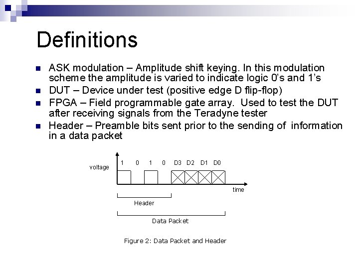
Definitions n n ASK modulation – Amplitude shift keying. In this modulation scheme the amplitude is varied to indicate logic 0’s and 1’s DUT – Device under test (positive edge D flip-flop) FPGA – Field programmable gate array. Used to test the DUT after receiving signals from the Teradyne tester Header – Preamble bits sent prior to the sending of information in a data packet voltage 1 0 D 3 D 2 D 1 D 0 time Header Data Packet Figure 2: Data Packet and Header
Definitions (cont. ) n n NRZ – Non-return to zero. Using NRZ, a logic 1 bit is sent as a high value and a logic 0 bit is sent as a low value. PLL – Phase-locked loop RZ – Return to zero. This is the opposite of NRZ data. The signal state is determined by the voltage during the first half of each data binary digit. The signal returns to a resting state (called zero) during the second half of each bit. Teradyne Integra J 750 – Tester donated to Iowa State University by Teradyne. It is used in the testing of printed circuit boards and integrated circuits.
Project Overview
Acknowledgement Dr. Weber n Nathaniel Gibbs n Jason Boyd n
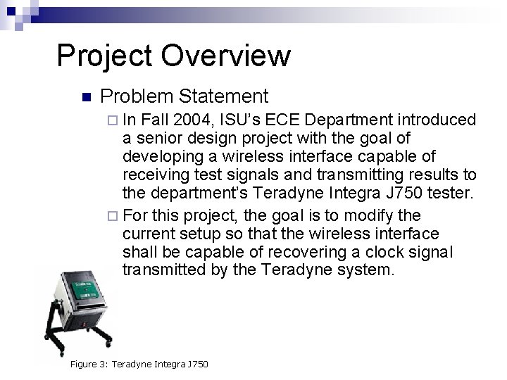
Project Overview n Problem Statement ¨ In Fall 2004, ISU’s ECE Department introduced a senior design project with the goal of developing a wireless interface capable of receiving test signals and transmitting results to the department’s Teradyne Integra J 750 tester. ¨ For this project, the goal is to modify the current setup so that the wireless interface shall be capable of recovering a clock signal transmitted by the Teradyne system. Figure 3: Teradyne Integra J 750
Project Overview n Assumptions A sufficient clock-training signal can be sent by the Teradyne J 750 over the S/R network to initialize the clock recovering circuitry. ¨ The clock recovering circuitry will be able to interact with the existing FPGA. ¨ The current wireless communication network can transmit up to five feet. This assumption is based on the May 05 team’s documentation. ¨ The phase difference between the system clock of the Teradyne J 750 and the recovered clock at the wireless interface will not be greater than the overall system clock frequency. ¨
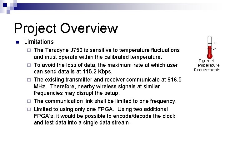
Project Overview n Limitations ¨ ¨ ¨ The Teradyne J 750 is sensitive to temperature fluctuations and must operate within the calibrated temperature. To avoid the loss of data, the maximum rate at which user can send data is at 115. 2 Kbps. The existing transmitter and receiver communicate at 916. 5 MHz. Therefore, nearby wireless signals at similar frequencies may disrupt the setup. The communication link shall be limited to one frequency. Limited to using only one FPGA. Using two additional FPGA’s, it would be possible to encode/decode the clock and test data into a single data stream. Figure 4: Temperature Requirements
Project Overview n Intended Users The user has knowledge in electrical and/or computer engineering. ¨ The user has previous experience testing circuits with the Teradyne J 750. ¨ n Intended Uses Functional test of a digital device ¨ (Future) Wireless chipset test ¨
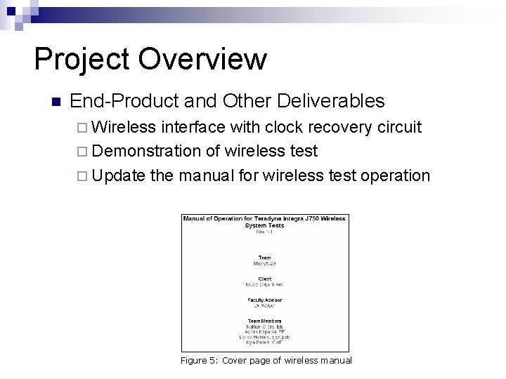
Project Overview n End-Product and Other Deliverables ¨ Wireless interface with clock recovery circuit ¨ Demonstration of wireless test ¨ Update the manual for wireless test operation Figure 5: Cover page of wireless manual
Project Activities
Previous Accomplishments n May 05 -29 Accomplishments ¨ Parallel-Serial Conversion ¨ Transmitters and Receivers ¨ Processing Device
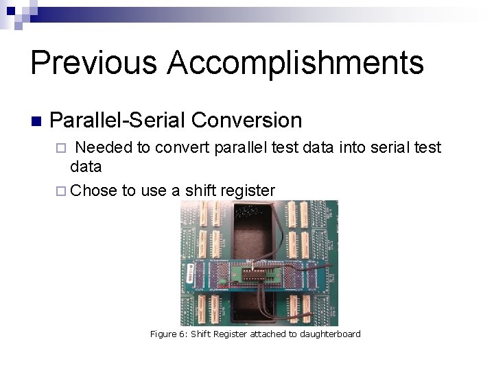
Previous Accomplishments n Parallel-Serial Conversion Needed to convert parallel test data into serial test data ¨ Chose to use a shift register ¨ Figure 6: Shift Register attached to daughterboard
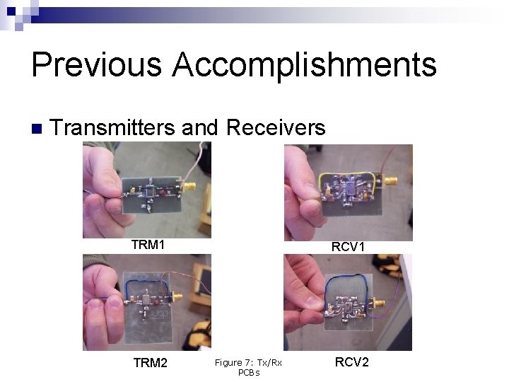
Previous Accomplishments n Transmitters and Receivers TRM 1 TRM 2 RCV 1 Figure 7: Tx/Rx PCBs RCV 2
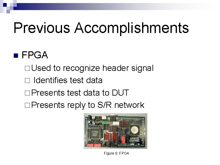
Previous Accomplishments n FPGA ¨ Used to recognize header signal ¨ Identifies test data ¨ Presents test data to DUT ¨ Presents reply to S/R network Figure 8: FPGA
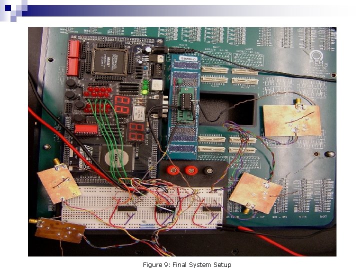
Figure 9: Final System Setup
Project Activities n Project Definition ¨ Part of the May 05 team’s project definition was to include a clock recovery circuit, but due to timing constraints was unable to do so. ¨ May 06 goal is to integrate a PLL for clock recovery with the existing network.
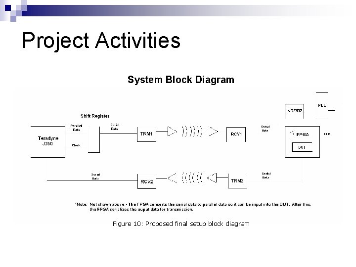
Project Activities System Block Diagram Figure 10: Proposed final setup block diagram
Project Activities n Technology Considerations ¨ Manchester vs. PLL ¨ NRZ to RZ Conversion
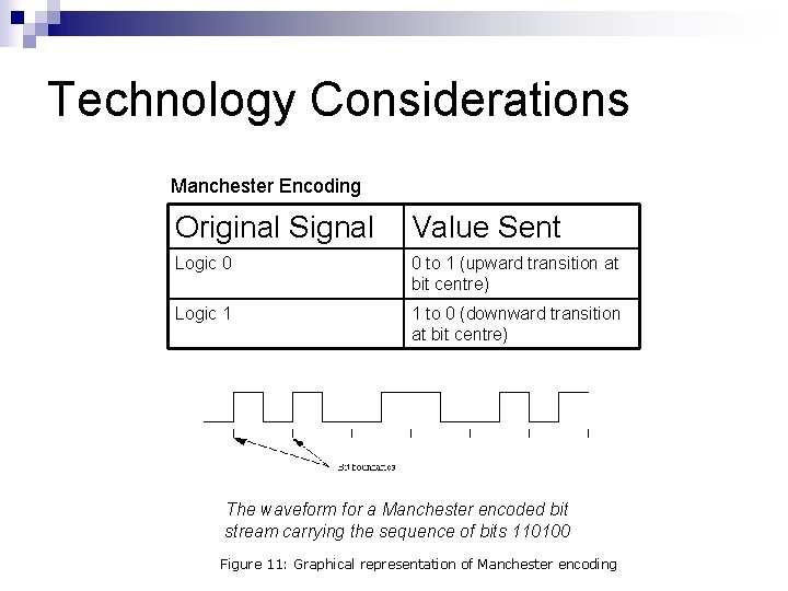
Technology Considerations Manchester Encoding Original Signal Value Sent Logic 0 0 to 1 (upward transition at bit centre) Logic 1 1 to 0 (downward transition at bit centre) The waveform for a Manchester encoded bit stream carrying the sequence of bits 110100 Figure 11: Graphical representation of Manchester encoding
Technology Considerations n Manchester Encoding ¨ Very easy to implement ¨ Clock phase and frequency are both present ¨ Too fast for current transmitters and receivers!
Technology Considerations n Phase Locked Loop ¨ Must be “trained” ¨ Test data must follow a training signal ¨ More difficult to implement ¨ Don’t have to build new transmitters and receivers
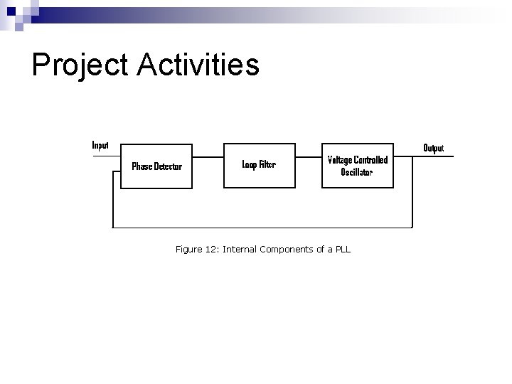
Project Activities Figure 12: Internal Components of a PLL
Project Activities n Phase Detector ¨ Type I – XOR ¨ *Type II – Generates lead or lag pulses n Voltage Controlled Oscillator (VCO) ¨ Centered at 115. 2 KHz ¨ Frequencies too far off of center frequency will not lock
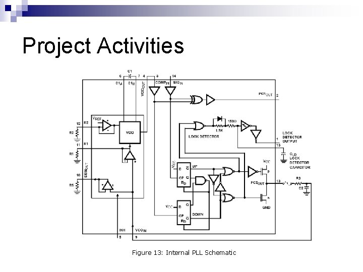
Project Activities Figure 13: Internal PLL Schematic
Project Activities n Monostable Multivibrators ¨ Chosen to convert NRZ data to RZ data ¨ Must use an external RC combination to specify pulse widths
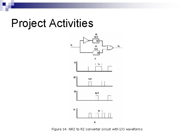
Project Activities Figure 14: NRZ to RZ converter circuit with I/O waveforms
Project Activities n Software ¨ FPGA serves as “brains” of system ¨ Verilog chosen by previous team to program FPGA ¨ New prototype code complete
Project Activities n Present Accomplishments üHardware Selected üPrevious team’s project setup and tested üPLL üMonostable Multivibrators ü Software Prototype control software for FPGA written ü IG-XL test template written ü
Project Activities n Planned Design/Test Activities ¨ ¨ ¨ Build and test NRZ to RZ converter Build and test PLL circuitry Put new circuitry on printed circuit board Modify FPGA code as necessary Test functional range of wireless interface
Resources & Schedule
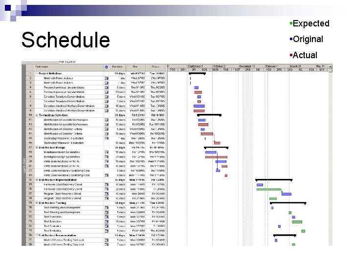
Schedule §Expected §Original §Actual
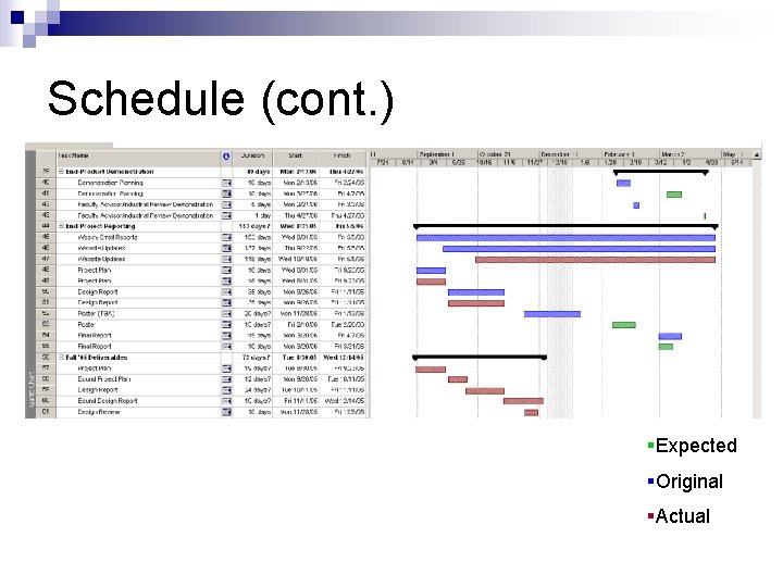
Schedule (cont. ) §Expected §Original §Actual
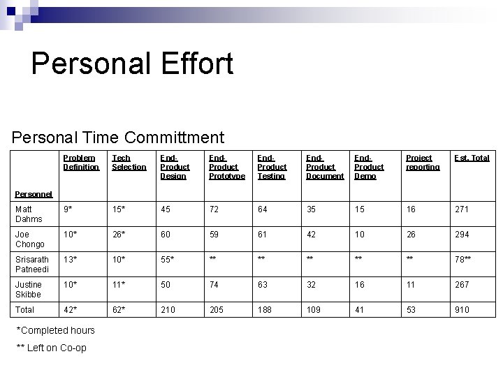
Personal Effort Personal Time Committment Problem Definition Tech Selection End. Product Design End. Product Prototype End. Product Testing End. Product Document End. Product Demo Project reporting Est. Total Matt Dahms 9* 15* 45 72 64 35 15 16 271 Joe Chongo 10* 26* 60 59 61 42 10 26 294 Srisarath Patneedi 13* 10* 55* ** ** ** 78** Justine Skibbe 10* 11* 50 74 63 32 16 11 267 Total 42* 62* 210 205 188 109 41 53 910 Personnel *Completed hours ** Left on Co-op
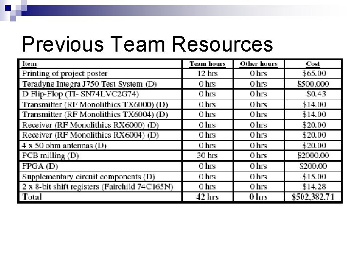
Previous Team Resources
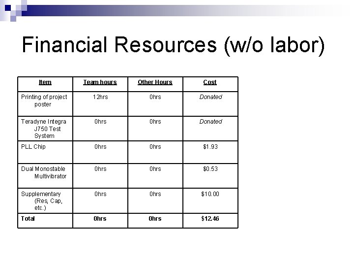
Financial Resources (w/o labor) Item Team hours Other Hours Cost Printing of project poster 12 hrs 0 hrs Donated Teradyne Integra J 750 Test System 0 hrs Donated PLL Chip 0 hrs $1. 93 Dual Monostable Multivibrator 0 hrs $0. 53 Supplementary (Res, Cap, etc. ) 0 hrs $10. 00 Total 0 hrs $12. 46
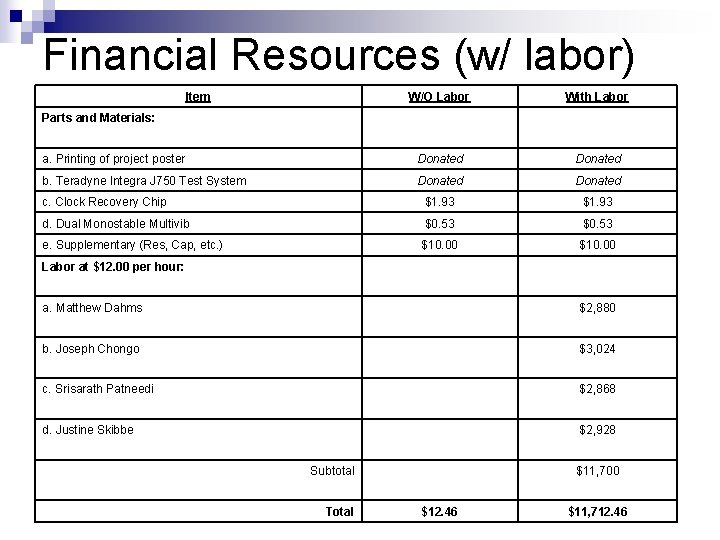
Financial Resources (w/ labor) Item W/O Labor With Labor a. Printing of project poster Donated b. Teradyne Integra J 750 Test System Donated c. Clock Recovery Chip $1. 93 d. Dual Monostable Multivib $0. 53 e. Supplementary (Res, Cap, etc. ) $10. 00 Parts and Materials: Labor at $12. 00 per hour: a. Matthew Dahms $2, 880 b. Joseph Chongo $3, 024 c. Srisarath Patneedi $2, 868 d. Justine Skibbe $2, 928 Subtotal Total $11, 700 $12. 46 $11, 712. 46
Closure Materials
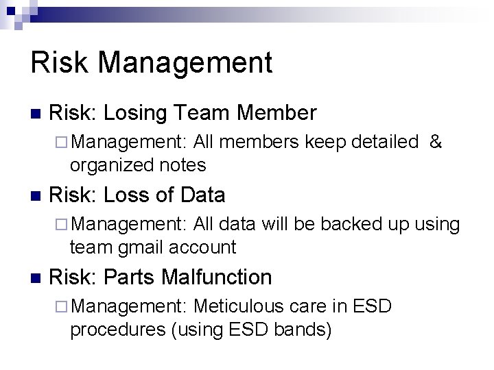
Risk Management n Risk: Losing Team Member ¨ Management: All members keep detailed & organized notes n Risk: Loss of Data ¨ Management: All data will be backed up using team gmail account n Risk: Parts Malfunction ¨ Management: Meticulous care in ESD procedures (using ESD bands)
Closing Materials n Lessons Learned ¨ What technical knowledge was gained? FPGA implementation n Teradyne Integra J 750 usage n Clock recovery methods n System integration n
Closing Materials n Lessons Learned ¨ What n n n May 05 System still works! Teamwork Learned to work in arctic environments (19 degrees C inside Teradyne lab) ¨ What n n went well? did not go well? Locating May 05 equipment Initial Teradyne J 750 setup and test Uploading program to FPGA input pins
Closing Materials n Closing Summary ¨ Problem – Integrate clock recovery circuitry into current system ¨ Solution Use PLL for clock recovery n Modify FPGA program to incorporate new components n
Questions? ? ?

Thank You
- Slides: 45