DEVELOPMENT TESTING ADC BOARD FOR THE PROMETEO TEST

DEVELOPMENT &TESTING: ADC BOARD FOR THE PROMETEO TEST BENCH MATTHEW SPOOR University of the Witwatersrand HEPP 2015

OVERVIEW ATLAS Tile Calorimeter Hybrid demonstrator Prometeo Test-bench Prometeo ADC board Outlook
 � 40 MHz bunch")
ATLAS DETECTOR � General purpose particle detector (Multiple sub- detectors) � 40 MHz bunch crossings � Petabytes of raw data per second � Preparing for Phase-II upgrade Tile Calorimeter

PHASE-II UPGRADE Present front-end electronics Equivalent Phase-II upgrade electronics Complete replacement of the front-end and back-end electronics introducing a new read-out architecture

HYBRID DEMONSTRATOR Validation of the new readout architecture, trigger system interfaces. Divides each Tile. Cal module into 4 independent minidrawers. Mini-drawer: Mainboard, Daughterboard, 12 PMTs, HV card and Adder board Compatible with old architecture. High level of redundancy

DEVELOPMENT OF THE ADC BOARD FPGA Testing Area in new Electronics Lab AIM: Test and Validate the design of the new ADC board. • Firmware needs to be re-designed to work on modern FPGAs. (Xilinx Virtex 7) • Identify and fix any design faults found in prototype design for next production. • Perform system function testing in new electronics Laboratory.

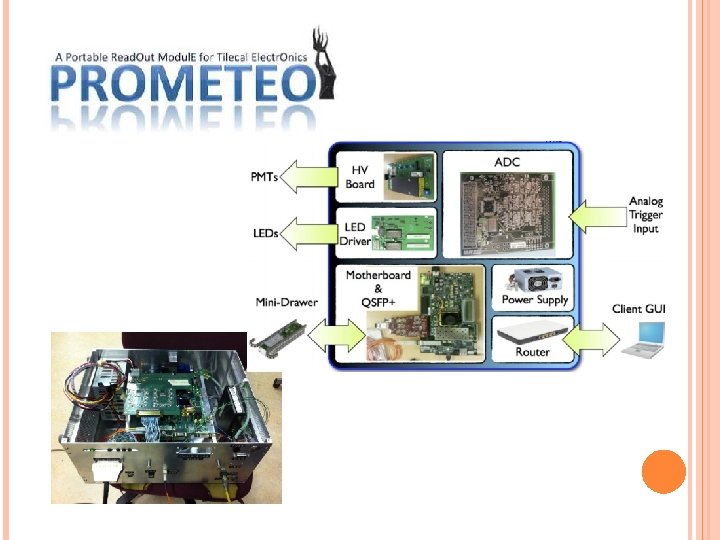
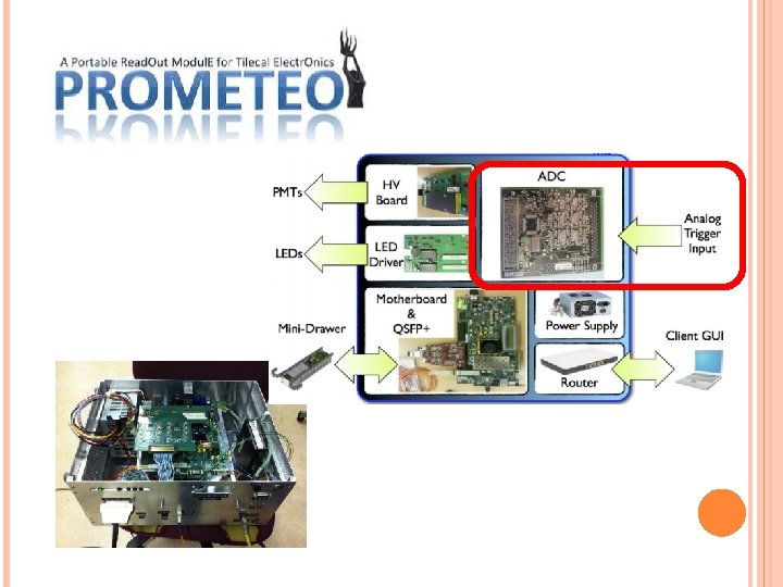
ADC BOARD Custom board that receives and digitises analog signals from the trigger outputs of the super drawer at 40 MHz Trigger data used for Hadron and Muon selection Four layer PCB with two ADS 5271 chips 8 -channel, 12 -bit, 50 MSPS analog-to-digital converters PCB redesigned to connect to the VC 707 via FMC connection LVPS channels transfer serialised data at 480 Mbps Prometeo ADC Mobi. DICK 4 ADC More than 2/3 size reduction

FIRMWARE New firmware had to be built to interface the ADC board with the Virtex 7 FPGA All FPGA firmware is designed using HDL Describes hardware interconnects Bit Level programming Non-sequential language Exceptionally efficient As the same ADCs chips themselves have not changed the similar design algorithms could be used. Data lines to/ from the ADC board. 16 Differential pairs for Data transfer (240 MHz) 8 Differential pairs for clock synchronisation 10 signals to ADC for board setup

FIRMWARE SIMULATIONS Precise timings needed to set up ADC chips correctly

CHIPSCOPE SIMULATIONS

CHIPSCOPE BOARD TESTING Clocking Issues: 40 MHz not reaching ADCs

FIXED CLOCKING PROBLEMS

PCB AND CIRCUIT DESIGN CHANGES • • • PCB redesigned to be compatible with VC 707 Dev board Improved power regulation systems Various component footprints changed. Repositioned indicator LEDs for easier viewing Component & Wire shifting to improve signal quality New 20 PIN output added to allow the Prometeo LED driver board to attach
")
OUTLOOK • Finalisation of next iteration of ADC board schematics and PCB design (Feb) • Get quotations for the production of 2 new ADCs boards (Feb) • Manufacture of the next ADC board prototype in South Africa (April) • Finalisation of firmware development (April) • Testing and validation of the next version of ADC board (July) Manufacture of 2 new ADC Boards

QUESTIONS?
- Slides: 17