Development of the CMS Silicon Strip Tracker Readout
- Slides: 12

Development of the CMS Silicon Strip Tracker Readout Matthew Noy Imperial College London 7 th April 2004, IOP, Birmingham

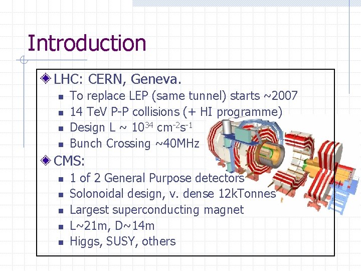
Introduction LHC: CERN, Geneva. n n To replace LEP (same tunnel) starts ~2007 14 Te. V P-P collisions (+ HI programme) Design L ~ 1034 cm-2 s-1 Bunch Crossing ~40 MHz CMS: n n n 1 of 2 General Purpose detectors Solonoidal design, v. dense 12 k. Tonnes Largest superconducting magnet L~21 m, D~14 m Higgs, SUSY, others

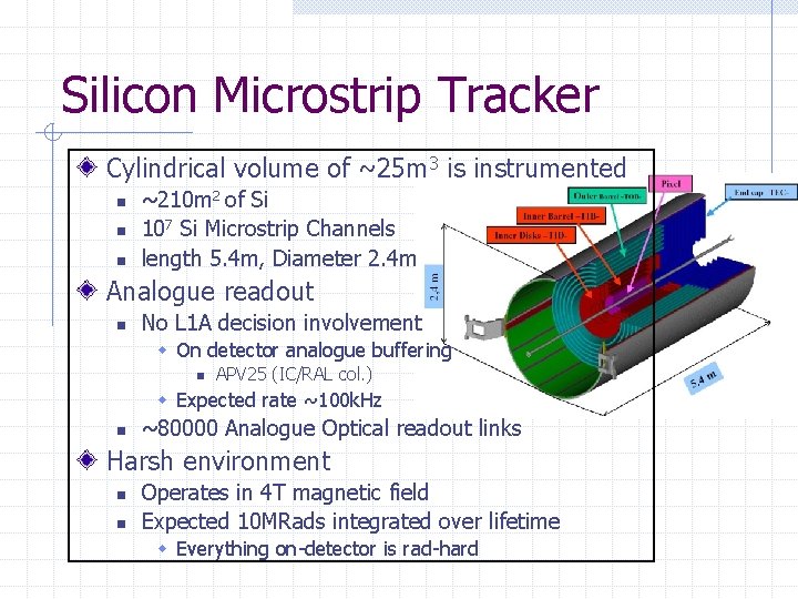
Silicon Microstrip Tracker Cylindrical volume of ~25 m 3 is instrumented n n n ~210 m 2 of Si 107 Si Microstrip Channels length 5. 4 m, Diameter 2. 4 m Analogue readout n No L 1 A decision involvement w On detector analogue buffering n APV 25 (IC/RAL col. ) w Expected rate ~100 k. Hz n ~80000 Analogue Optical readout links Harsh environment n n Operates in 4 T magnetic field Expected 10 MRads integrated over lifetime w Everything on-detector is rad-hard

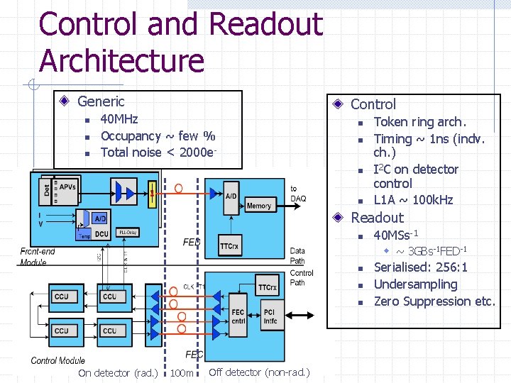
Control and Readout Architecture Generic n n n 40 MHz Occupancy ~ few % Total noise < 2000 e- Control n n Token ring arch. Timing ~ 1 ns (indv. ch. ) I 2 C on detector control L 1 A ~ 100 k. Hz Readout n 40 MSs-1 w ~ 3 GBs-1 FED-1 n n n On detector (rad. ) 100 m Off detector (non-rad. ) Serialised: 256: 1 Undersampling Zero Suppression etc.

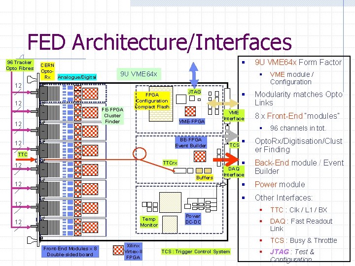
FED Architecture/Interfaces 96 Tracker Opto Fibres CERN Opto. Rx Analogue/Digital § 9 U VME 64 x Form Factor § 9 U VME 64 x 12 12 FE-FPGA Cluster Finder 12 JTAG FPGA Configuration Compact Flash VME-FPGA § VME Interface § Modularity matches Opto Links 8 x Front-End “modules” § BE-FPGA Event Builder 12 TCS TTCrx Buffers Opto. Rx/Digitisation/Clust er Finding § Back-End module / Event Builder § Power module § Other Interfaces: DAQ Interface 12 12 Temp Monitor 12 Front-End Modules x 8 Double-sided board Xilinx Virtex-II FPGA Power DC-DC TCS : Trigger Control System 96 channels in tot. § TTC 12 VME module / Configuration § TTC : Clk / L 1 / BX § DAQ : Fast Readout Link § TCS : Busy & Throttle § JTAG : Test & Configuration

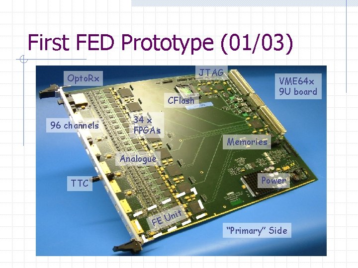
First FED Prototype (01/03) JTAG Opto. Rx VME 64 x 9 U board CFlash 96 channels 34 x FPGAs Memories Analogue Power TTC t F ni U E “Primary” Side

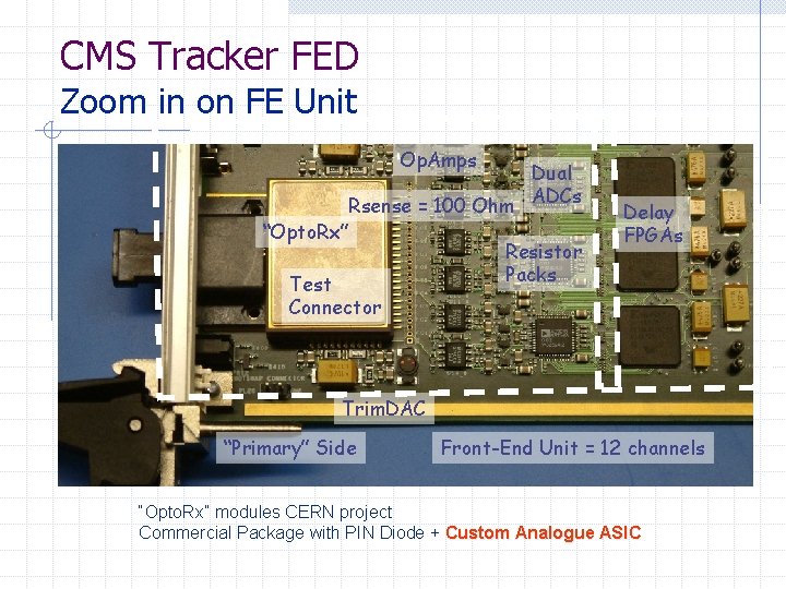
CMS Tracker FED Zoom in on FE Unit Op. Amps Dual Rsense = 100 Ohm ADCs “Opto. Rx” Resistor Packs Test Delay FPGAs Connector Trim. DAC “Primary” Side Front-End Unit = 12 channels “Opto. Rx” modules CERN project Commercial Package with PIN Diode + Custom Analogue ASIC

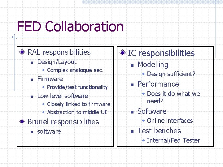
FED Collaboration RAL responsibilities n Design/Layout w Complex analogue sec. n n software Software w Online interfaces Brunel responsibilities n Performance w Does it do what we need? Low level software w Closely linked to firmware w Abstraction to middle UI Modelling w Design sufficient? Firmware w Provide/test functionality n IC responsibilities n Test benches w Internal/Fed Tester

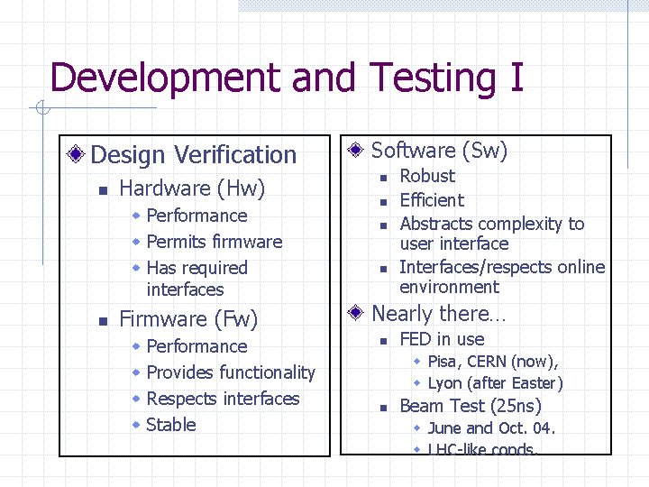
Development and Testing I Design Verification n Hardware (Hw) w Performance w Permits firmware w Has required interfaces n Firmware (Fw) w w Performance Provides functionality Respects interfaces Stable Software (Sw) n n Robust Efficient Abstracts complexity to user interface Interfaces/respects online environment Nearly there… n FED in use w Pisa, CERN (now), w Lyon (after Easter) n Beam Test (25 ns) w June and Oct. 04. w LHC-like conds.

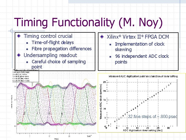
Timing Functionality (M. Noy) Timing control crucial n n Time-of-flight delays Fibre propagation differences Undersampling readout n Careful choice of sampling point Xilinx Virtex II FPGA DCM n n Implementation of clock skewing 96 independent ADC clock points 32 fine steps of ~ 800 psec

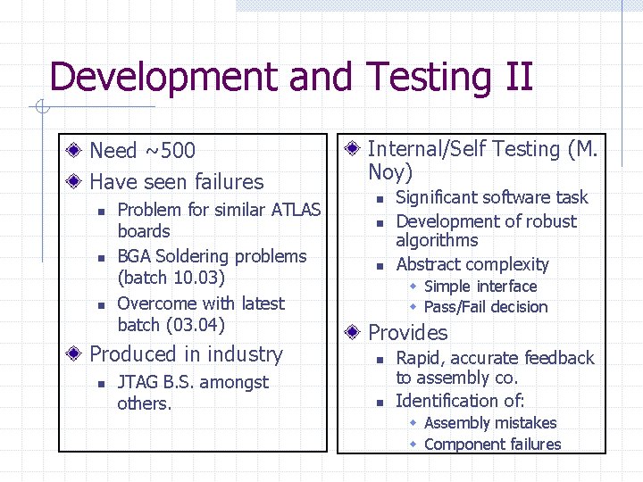
Development and Testing II Need ~500 Have seen failures n n n Problem for similar ATLAS boards BGA Soldering problems (batch 10. 03) Overcome with latest batch (03. 04) Produced in industry n JTAG B. S. amongst others. Internal/Self Testing (M. Noy) n n n Significant software task Development of robust algorithms Abstract complexity w Simple interface w Pass/Fail decision Provides n n Rapid, accurate feedback to assembly co. Identification of: w Assembly mistakes w Component failures

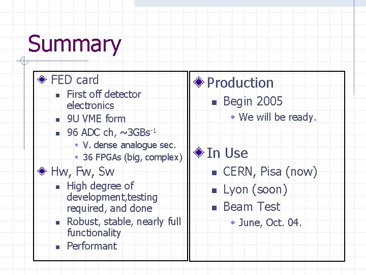
Summary FED card n n n First off detector electronics 9 U VME form 96 ADC ch, ~3 GBs-1 w V. dense analogue sec. w 36 FPGAs (big, complex) Hw, Fw, Sw n n n High degree of development, testing required, and done Robust, stable, nearly full functionality Performant Production n Begin 2005 w We will be ready. In Use n n n CERN, Pisa (now) Lyon (soon) Beam Test w June, Oct. 04.