
Development of STJ with FDSOI cryogenic amplifier as


- Slides: 33
Development of STJ with FD-SOI cryogenic amplifier as a far-infrared single photon detector for COBAND experiment 17 th International workshop on Low Temperature d Detectors (LTD 17) Jul. 17 -21, 2017 / Kurume City Plaza, Kurume Yuji Takeuchi (Univ. of Tsukuba) S. -H. Kim, T. Iida, K. Takemasa, K. Nagata, C. Asano, S. Yagi, R. Wakasa (U of Tsukuba), H. Ikeda, T. Wada, K. Nagase (ISAS/JAXA), S. Matsuura (Kwansei gakuin U), Y. Arai, I. Kurachi, M. Hazumi (KEK), T. Yoshida, T. Nakamura, M. Sakai, W. Nishimura (U of Fukui), S. Mima, K. Kiuchi (RIKEN), H. Ishino, A. Kibayashi (Okayama U), Y. Kato (Kindai U), G. Fujii, S. Shiki, M. Ukibe, M. Ohkubo (AIST), S. Kawahito (Shizuoka U), E. Ramberg, P. Rubinov, D. Sergatskov (FNAL), S. -B. Kim (Seoul National U) COBAND collaboration 1
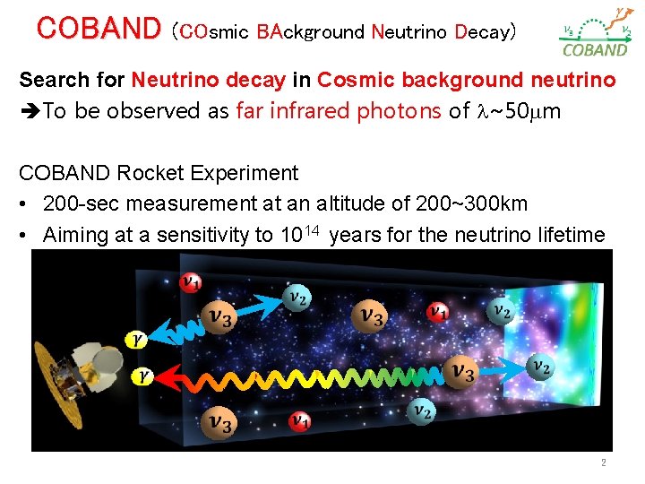
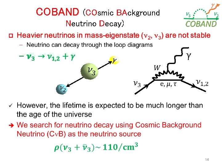
COBAND (COsmic BAckground Neutrino Decay) Search for Neutrino decay in Cosmic background neutrino To be observed as far infrared photons of ~50 m COBAND Rocket Experiment • 200 -sec measurement at an altitude of 200~300 km • Aiming at a sensitivity to 1014 years for the neutrino lifetime 2
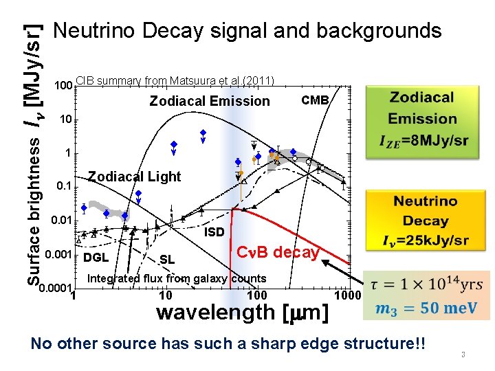
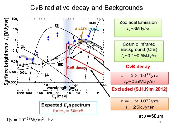
[MJy/sr] Neutrino Decay signal and backgrounds 100 CIB summary from Matsuura et al. (2011) Surface brightness I Zodiacal Emission CMB 10 1 0. 1 Zodiacal Light 0. 01 ISD 0. 001 DGL 0. 0001 1 SL C B decay Integrated flux from galaxy counts 10 100 wavelength [ m] 1000 No other source has such a sharp edge structure!! 3
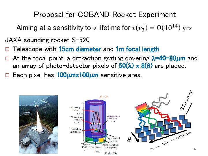
Proposal for COBAND Rocket Experiment ST Ja rra y JAXA sounding rocket S-520 ¨ Telescope with 15 cm diameter and 1 m focal length ¨ At the focal point, a diffraction grating covering =40 -80 m and an array of photo-detector pixels of 50( ) x 8( ) are placed. ¨ Each pixel has 100 mx 100 m sensitive area. 4
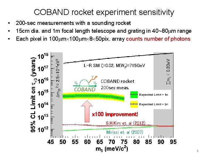
COBAND rocket experiment sensitivity L-R SM =0. 02, M(W 2)=715 Ge. V COBAND rocket 200 sec meas. mi < 0. 23 e. V 200 -sec measurements with a sounding rocket 15 cm dia. and 1 m focal length telescope and grating in 40~80 m range Each pixel in 100 m 8 50 pix. array counts number of photons m 312 = 2. 5 10 -3 e. V 2 • • • x 100 improvement! S. H. Kim et. al (2012) Mirizzi et. al (2007) 5
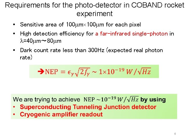
Requirements for the photo-detector in COBAND rocket experiment • Sensitive area of 100 m for each pixel • High detection efficiency for a far-infrared single-photon in =40 m~ 80 m • Dark count rate less than 300 Hz (expected real photon rate) 6
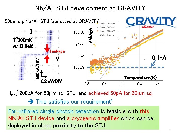
Nb/Al-STJ development at CRAVITY I 100 n. A T~300 m. K w/ B field 10 n. A Leakage 50 m sq. Nb/Al-STJ fabricated at CRAVITY 500 p. A/DIV Leakage V 1 n. A 0. 1 n. A 100 p. A 0. 2 m. V/DIV Temperature(K) 0. 3 0. 4 0. 5 0. 6 0. 7 Ileak~200 p. A for 50 m sq. STJ, and achieved 50 p. A for 20 m sq. This satisfies our requirement! Far-infrared single photon detection is feasible with this Nb/Al-STJ device and a cryogenic amplifier which can be deployed in close proximity to the STJ. 7
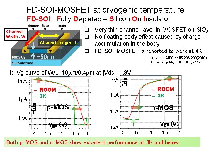
FD-SOI-MOSFET at cryogenic temperature FD-SOI : Fully Depleted – Silicon On Insulator Channel Width : W Channel Length : L ~50 nm p Very thin channel layer in MOSFET on Si. O 2 p No floating body effect caused by charge accumulation in the body p FD-SOI-MOSFET is reported to work at 4 K JAXA/ISIS AIPC 1185, 286 -289(2009) J Low Temp Phys 167, 602 (2012) 1 m. A ROOM 3 K -Ids 1 A p-MOS Ids Id-Vg curve of W/L=10 m/0. 4 m at |Vds|=1. 8 V 1 A ROOM 3 K 1 n. A n-MOS 1 n. A Vgs (V) -2 -1. 5 -1 Vgs (V) 1 p. A -0. 5 0 0 0. 5 1 1. 5 2 Both p-MOS and n-MOS show excellent performance at 3 K and below. 8
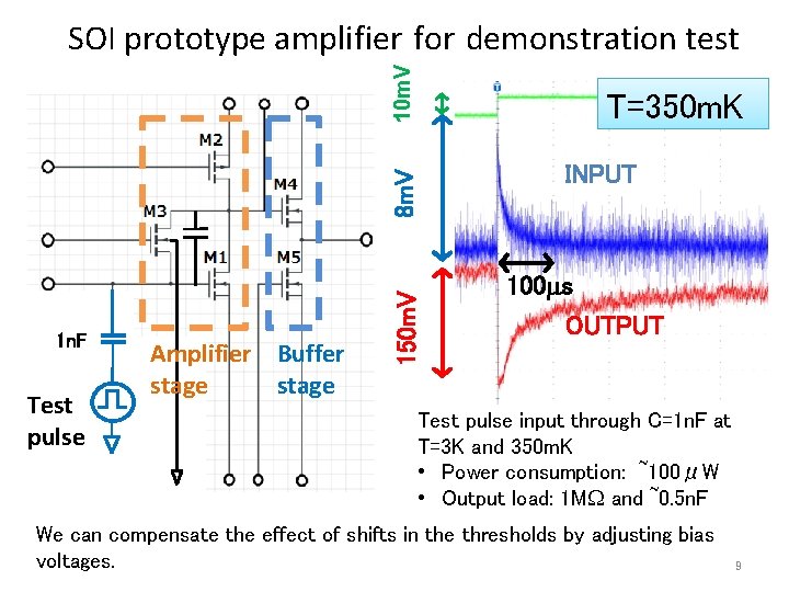
10 m. V SOI prototype amplifier for demonstration test T=350 m. K 1 n. F V Test pulse Amplifier Buffer stage 150 m. V 8 m. V INPUT 100 s OUTPUT Test pulse input through C=1 n. F at T=3 K and 350 m. K • Power consumption: ~100μW • Output load: 1 M and ~0. 5 n. F We can compensate the effect of shifts in the thresholds by adjusting bias voltages. 9
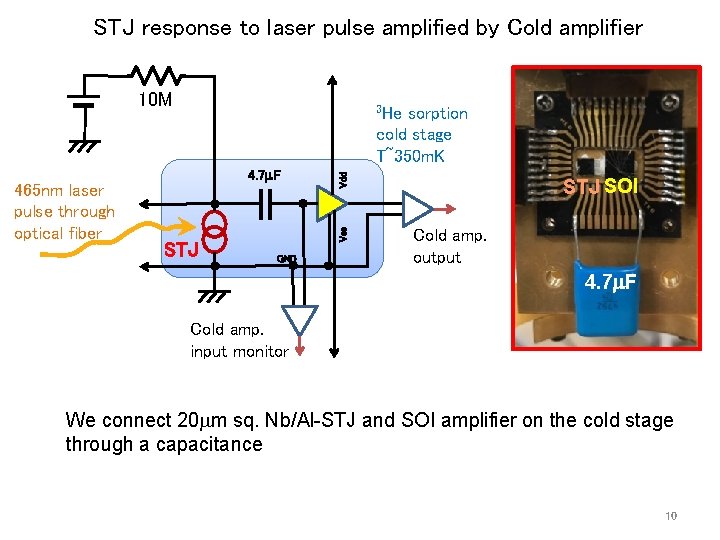
STJ response to laser pulse amplified by Cold amplifier 10 M 4. 7 F STJ Vdd sorption cold stage T~350 m. K Vss 465 nm laser pulse through optical fiber 3 He GND STJ SOI Cold amp. output 4. 7 F Cold amp. input monitor We connect 20 m sq. Nb/Al-STJ and SOI amplifier on the cold stage through a capacitance 10
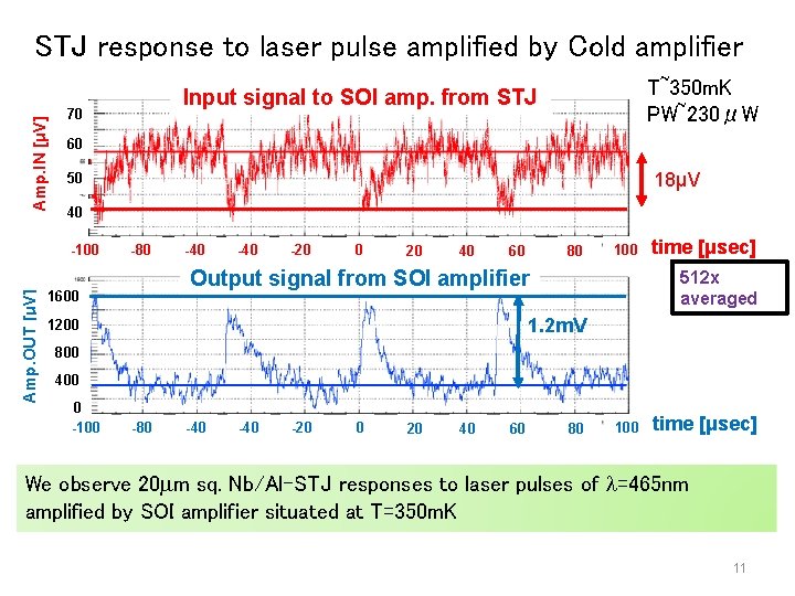
Amp. IN [μV] STJ response to laser pulse amplified by Cold amplifier 70 60 18μV 50 40 -100 Amp. OUT [μV] T~350 m. K PW~230μW Input signal to SOI amp. from STJ -80 -40 -20 0 20 40 80 60 100 Output signal from SOI amplifier 1600 time [μsec] 512 x averaged 1. 2 m. V 1200 800 400 0 -100 -80 -40 -20 0 20 40 60 80 100 time [μsec] We observe 20 m sq. Nb/Al-STJ responses to laser pulses of =465 nm amplified by SOI amplifier situated at T=350 m. K 11
Summary • We propose COBAND experiment to search for neutrino radiative decay in cosmic neutrino background. • Requirements for the detector is a photo-detector with NEP~10 -19 W/ Hz. • Nb/Al-STJ array with a diffractive for the sounding rocket experiment. – Nb/Al-STJs fabricated at CRAVITY satisfy our requirements. – Cryogenic FD-SOI amplifiers are under development and we demonstrated STJ signal amplification by a prototype SOI amplifier at T~350 m. K. • Improvement of the neutrino lifetime lower limit up to O(1014 yrs) is feasible for 200 -sec measurement in a rocket-borne experiment with the detector. * SOI design in this work is supported by VDEC, the U. Tokyo in collaboration with Synopsys, Inc. , Cadence Design Systems, Inc. , and Mentor Graphics, Inc. 12
Backup 13
COBAND (COsmic BAckground Neutrino Decay) 14
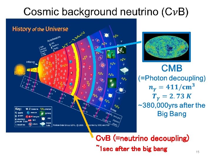
C B (=neutrino decoupling) ~1 sec after the big bang 15
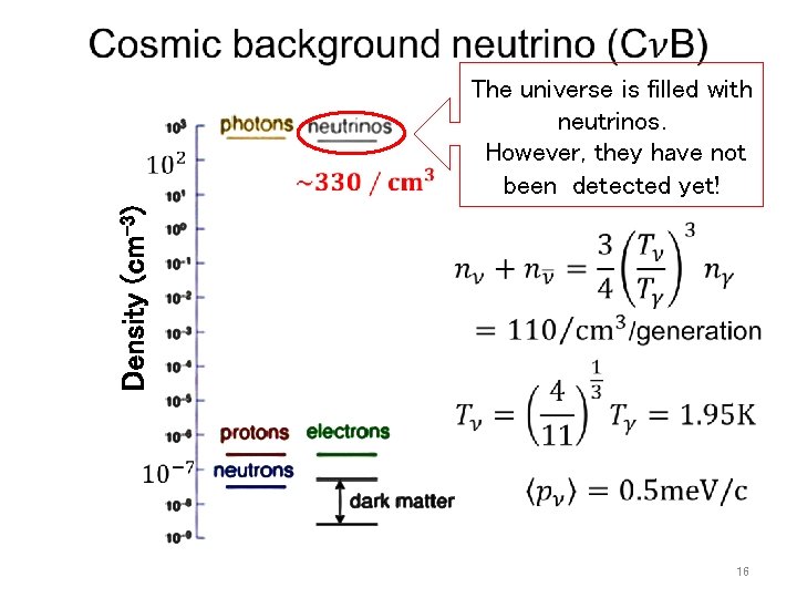
Density (cm-3) The universe is filled with neutrinos. However, they have not been detected yet! 16
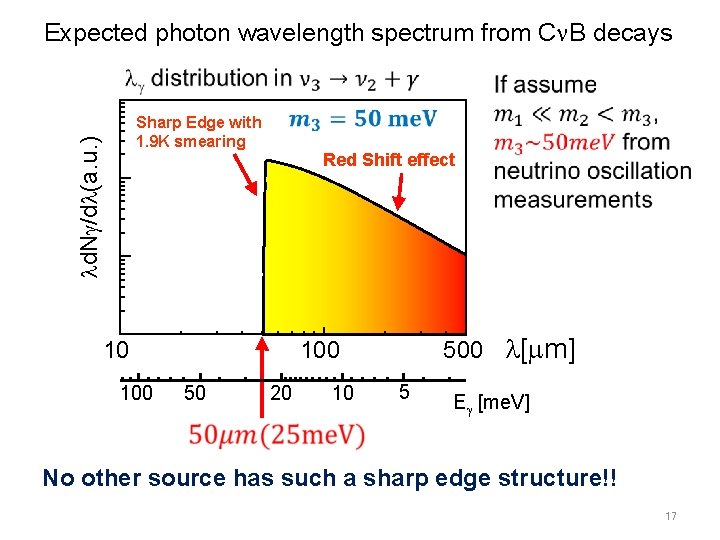
Expected photon wavelength spectrum from C B decays d. N /d (a. u. ) Sharp Edge with 1. 9 K smearing Red Shift effect 10 100 500 [ m] 100 50 20 10 5 E [me. V] No other source has such a sharp edge structure!! 17
Surface brightness I [MJy/sr] 100 CMB ZE AKARI COBE 10 1 ZL 0. 1 0. 01 ISD 0. 001 DGL SL 0. 0001 1 1000 500 C B decay 10 100 wavelength [ m] 200 100 50 E [me. V] 20 10 5 2 Excluded (S. H. Kim 2012) at λ= 50μm 18
19 COBAND Collaboration Members (As of Jul. 2017) Shin-Hong Kim, Yuji Takeuchi, Hideki Okawa, Takashi Iida, Kenichi Takemasa, Kazuki Nagata, Chisa Asano, Rena Wakasa, Yoichi Otsuka (Univ. of Tsukuba), Hirokazu Ikeda, Takehiko Wada, Koichi Nagase (JAXA/ISAS), Shuji Matsuura (Kwansei gakuin Univ), Yasuo Arai, Ikuo Kurachi, Masashi Hazumi (KEK), Takuo Yoshida,Takahiro Nakamura, Makoto Sakai, Wataru Nishimura (Univ. of Fukui), Satoshi Mima, Kenji Kiuchi (RIKEN), H. Ishino, A. Kibayashi (Okayama Univ. ), Yukihiro Kato (Kindai University), Go Fujii, Shigetomo Shiki, Masahiro Ukibe, Masataka Ohkubo (AIST), Shoji Kawahito (Shizuoka Univ. ), Erik Ramberg, Paul Rubinov, Dmitri Sergatskov (Fermilab), Soo-Bong Kim (Seoul National University) 19
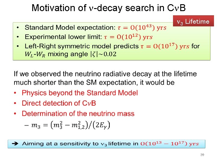
Motivation of -decay search in C B 3 Lifetime • 20
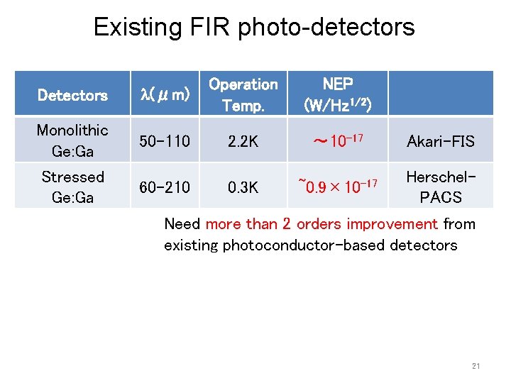
Existing FIR photo-detectors Detectors (μm) Operation Temp. NEP (W/Hz 1/2) Monolithic Ge: Ga 50 -110 2. 2 K ~ 10 -17 Akari-FIS Stressed Ge: Ga 60 -210 0. 3 K ~0. 9× 10 -17 Herschel. PACS Need more than 2 orders improvement from existing photoconductor-based detectors 21
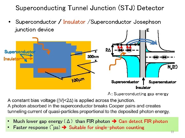
Superconducting Tunnel Junction (STJ) Detector • Superconductor / Insulator /Superconductor Josephson junction device E 2 Superconductor 300 nm Insulator Ns(E) 100 m Superconductor Insulator Δ: Superconducting gap energy • Much lower gap energy (Δ) than FIR photon Can detect FIR photon • Faster response (~ s) Suitable for single-photon counting 22
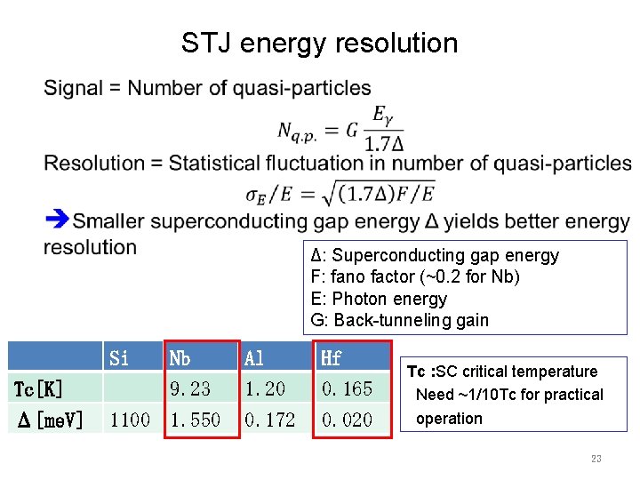
STJ energy resolution Δ: Superconducting gap energy F: fano factor (~0. 2 for Nb) E: Photon energy G: Back-tunneling gain Si Tc[K] Δ[me. V] Nb Al Hf 9. 23 1. 20 0. 165 0. 172 0. 020 1100 1. 550 Tc : SC critical temperature Need ~1/10 Tc for practical operation 23
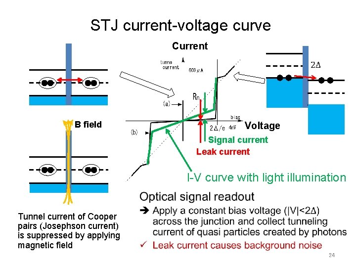
STJ current-voltage curve Current B field Voltage Signal current Leak current I-V curve with light illumination • Tunnel current of Cooper pairs (Josephson current) is suppressed by applying magnetic field 24
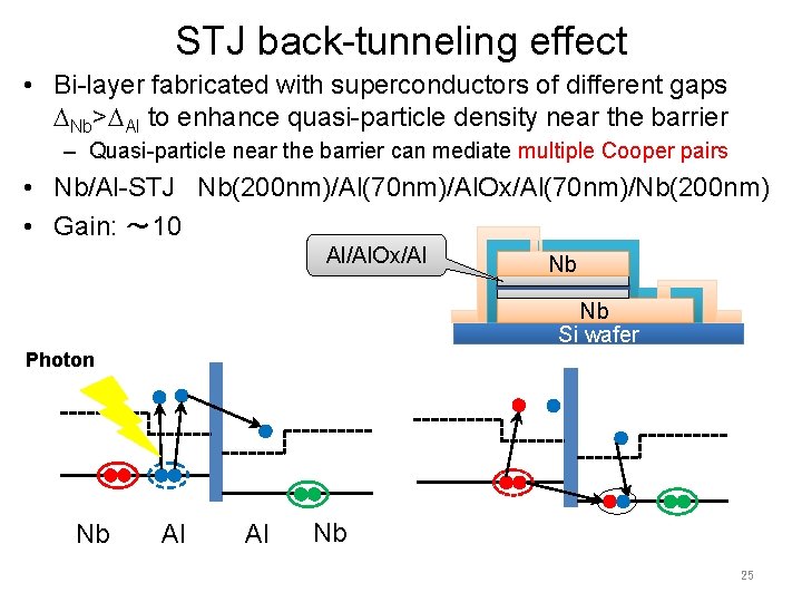
STJ back-tunneling effect • Bi-layer fabricated with superconductors of different gaps Nb> Al to enhance quasi-particle density near the barrier – Quasi-particle near the barrier can mediate multiple Cooper pairs • Nb/Al-STJ Nb(200 nm)/Al(70 nm)/Al. Ox/Al(70 nm)/Nb(200 nm) • Gain: ~ 10 Al/Al. Ox/Al Nb Nb Si wafer Photon Nb Al Al Nb 25
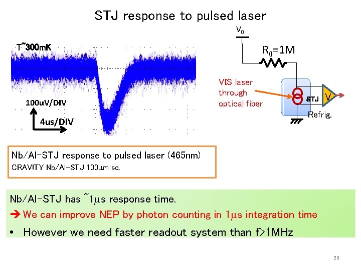
STJ response to pulsed laser V 0 T~300 m. K 100 u. V/DIV R 0=1 M VIS laser through optical fiber 4 us/DIV STJ V Refrig. Nb/Al-STJ response to pulsed laser (465 nm) CRAVITY Nb/Al-STJ 100 m sq. Nb/Al-STJ has ~1 s response time. We can improve NEP by photon counting in 1 s integration time • However we need faster readout system than f>1 MHz 26
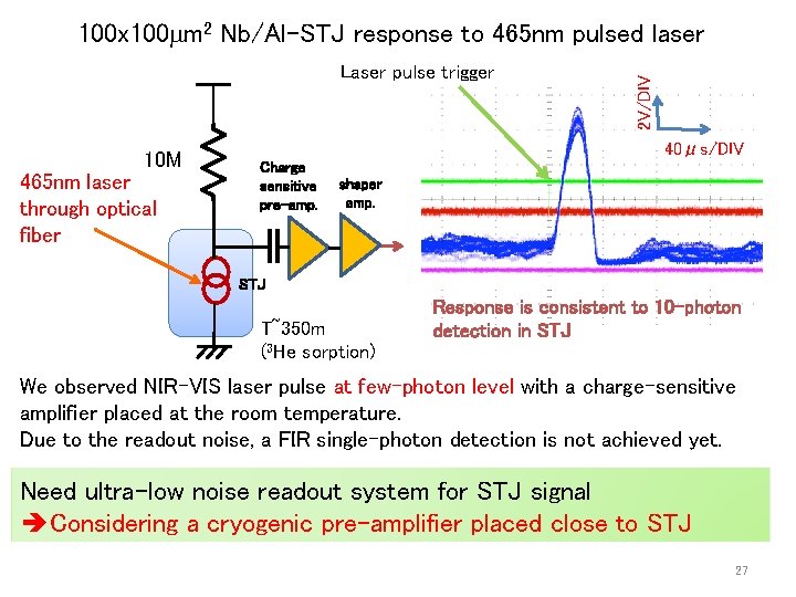
Laser pulse trigger 10 M 465 nm laser through optical fiber 2 V/DIV 100 x 100 m 2 Nb/Al-STJ response to 465 nm pulsed laser 40μs/DIV Charge sensitive pre-amp. shaper amp. STJ T~350 m (3 He sorption) Response is consistent to 10 -photon detection in STJ We observed NIR-VIS laser pulse at few-photon level with a charge-sensitive amplifier placed at the room temperature. Due to the readout noise, a FIR single-photon detection is not achieved yet. Need ultra-low noise readout system for STJ signal Considering a cryogenic pre-amplifier placed close to STJ 27
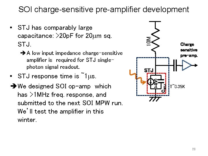
• STJ response time is ~1 s. We designed SOI op-amp which has >1 MHz freq. response, and submitted to the next SOI MPW run. We’ll test the amplifier in this winter. STJ CSTJ A low input impedance charge-sensitive amplifier is required for STJ singlephoton signal readout. Charge sensitive pre-amp. I=I(V) • STJ has comparably large capacitance: >20 p. F for 20 m sq. STJ. 10 M SOI charge-sensitive pre-amplifier development T~0. 35 K 28
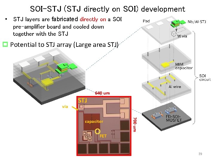
SOI-STJ (STJ directly on SOI) development • STJ layers are fabricated directly on a SOI pre-amplifier board and cooled down together with the STJ p Potential to STJ array (Large area STJ) via STJ 640 um 700 um capacitor FET 29
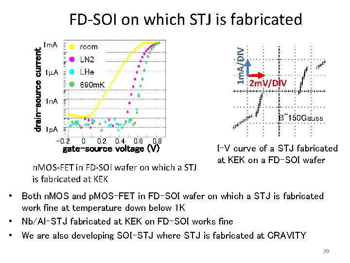
1 m. A/DIV drain-source current FD-SOI on which STJ is fabricated 1 A 2 m. V/DIV 1 n. A B~150 Gauss 1 p. A -0. 2 0. 4 0. 6 0. 8 gate-source voltage (V) n. MOS-FET in FD-SOI wafer on which a STJ is fabricated at KEK I-V curve of a STJ fabricated at KEK on a FD-SOI wafer • Both n. MOS and p. MOS-FET in FD-SOI wafer on which a STJ is fabricated work fine at temperature down below 1 K • Nb/Al-STJ fabricated at KEK on FD-SOI works fine • We are also developing SOI-STJ where STJ is fabricated at CRAVITY 30
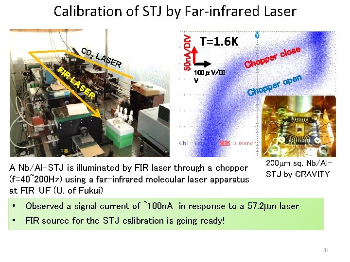
CO 2 FI R LA SE R LAS ER 50 n. A/DIV Calibration of STJ by Far-infrared Laser T=1. 6 K 100μV/DI V se lo c r e hopp C op r e p p en Cho A Nb/Al-STJ is illuminated by FIR laser through a chopper (f=40~200 Hz) using a far-infrared molecular laser apparatus at FIR-UF (U. of Fukui) 200 m sq. Nb/Al. STJ by CRAVITY • Observed a signal current of ~100 n. A in response to a 57. 2 m laser • FIR source for the STJ calibration is going ready! 31
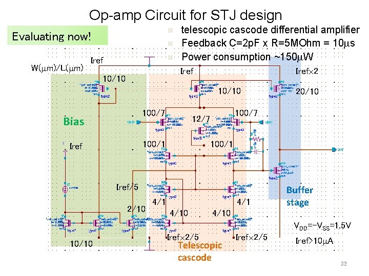
Op-amp Circuit for STJ design n Evaluating now! W( m)/L( m) n n Iref telescopic cascode differential amplifier Feedback C=2 p. F x R=5 MOhm = 10 s Power consumption ~150 W Iref 2 Iref 10/10 100/7 Bias 100/7 12/7 100/1 Iref/5 2/10 20/10 4/1 4/10 Buffer stage 4/10 VDD=-VSS=1. 5 V 10/10 Iref 2/5 Telescopic cascode Iref 2/5 Iref>10 A 32
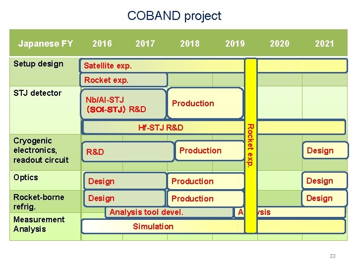
COBAND project Japanese FY Setup design 2016 2017 2018 2019 2020 2021 Satellite exp. Rocket exp. STJ detector Production Hf-STJ R&D Nb/Al-STJ設計・開発 Production R&D Rocket exp. Cryogenic electronics, readout circuit Nb/Al-STJ (SOI-STJ) R&D Design Optics Design Production Design Rocket-borne refrig. Design Production Design Measurement Analysis tool devel. Analysis Simulation 33