Development of highZ sensors for pixel array detectors


- Slides: 33

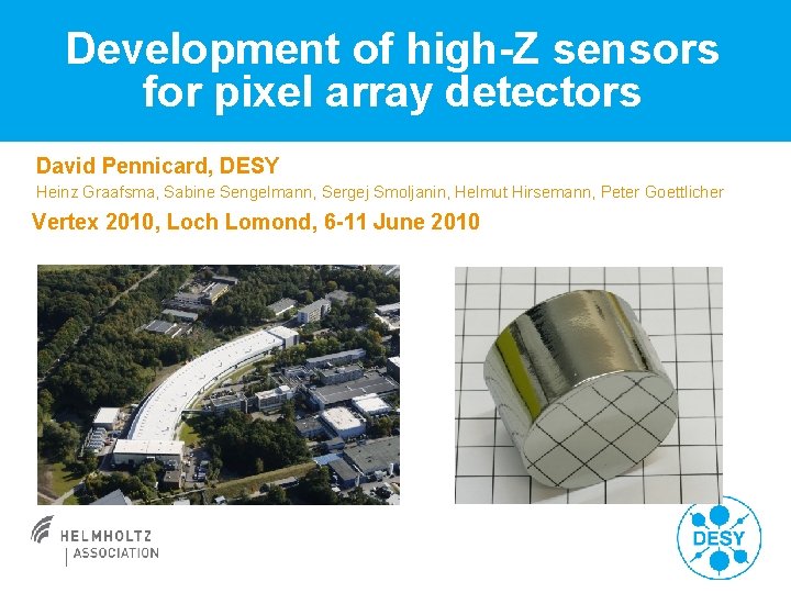
Development of high-Z sensors for pixel array detectors David Pennicard, DESY Heinz Graafsma, Sabine Sengelmann, Sergej Smoljanin, Helmut Hirsemann, Peter Goettlicher Vertex 2010, Loch Lomond, 6 -11 June 2010

Development of high-Z sensors for pixel array detectors > Applications of high-Z pixel arrays > Overview of high-Z sensors § Cd. Te / CZT § Ga. As > Work on pixellated Ge sensors at DESY > Summary David Pennicard | Development of high-Z sensors for pixel array detectors| Vertex 2010, Loch Lomond, 6 -11 June 2010 | Page 2

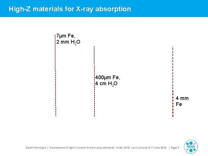
High-Z materials for X-ray absorption 7μm Fe, 2 mm H 2 O 400μm Fe, 4 cm H 2 O 4 mm Fe David Pennicard | Development of high-Z sensors for pixel array detectors| Vertex 2010, Loch Lomond, 6 -11 June 2010 | Page 3

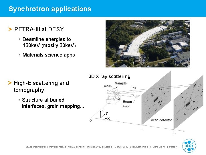
Synchrotron applications > PETRA-III at DESY § Beamline energies to 150 ke. V (mostly 50 ke. V) § Materials science apps > High-E scattering and tomography 3 D X-ray scattering § Structure at buried interfaces, grain mapping. . . David Pennicard | Development of high-Z sensors for pixel array detectors| Vertex 2010, Loch Lomond, 6 -11 June 2010 | Page 4

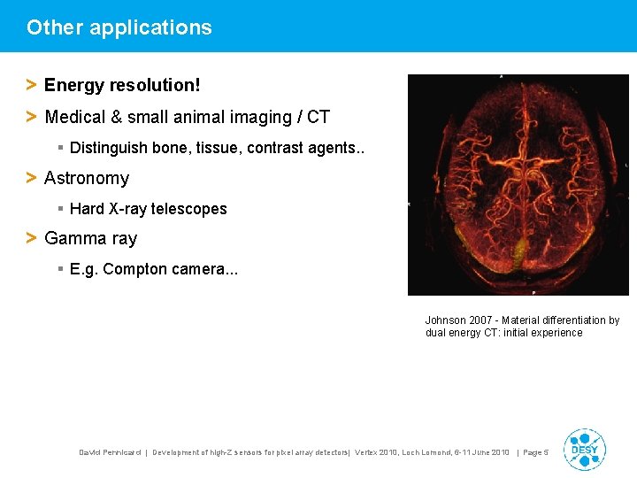
Other applications > Energy resolution! > Medical & small animal imaging / CT § Distinguish bone, tissue, contrast agents. . > Astronomy § Hard X-ray telescopes > Gamma ray § E. g. Compton camera. . . Johnson 2007 - Material differentiation by dual energy CT: initial experience David Pennicard | Development of high-Z sensors for pixel array detectors| Vertex 2010, Loch Lomond, 6 -11 June 2010 | Page 5

Collaborations > Hi. ZPAD (Hi-Z sensors for Pixel Array Detectors) § ESRF (coordinator), CNRS/D 2 AM, DESY, DLS, ELETTRA, PSI/SLS, SOLEIL § CPPM, RAL, University of Freiburg FMF, University of Surrey, DECTRIS > Medipix 3 § See Richard Plackett’s talk § Inter-pixel communication allows thick high-Z sensors David Pennicard | Development of high-Z sensors for pixel array detectors| Vertex 2010, Loch Lomond, 6 -11 June 2010 | Page 6

Development of high-Z sensors for pixel array detectors > Applications of high-Z pixel arrays > Overview of high-Z sensors § Cd. Te / CZT § Ga. As > Work on pixellated Ge sensors at DESY > Summary David Pennicard | Development of high-Z sensors for pixel array detectors| Vertex 2010, Loch Lomond, 6 -11 June 2010 | Page 7

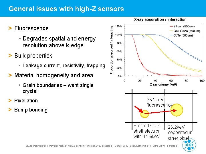
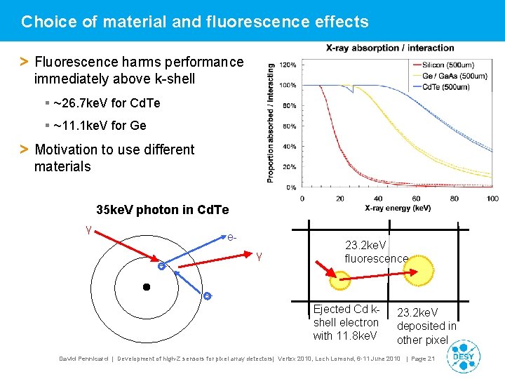
General issues with high-Z sensors > Fluorescence § Degrades spatial and energy resolution above k-edge > Bulk properties § Leakage current, resistivity, trapping > Material homogeneity and area § Grain boundaries – want single crystal > Pixellation > Bump bonding 23. 2 ke. V fluorescence Ejected Cd kshell electron with 11. 8 ke. V 23. 2 ke. V deposited in other pixel David Pennicard | Development of high-Z sensors for pixel array detectors| Vertex 2010, Loch Lomond, 6 -11 June 2010 | Page 8

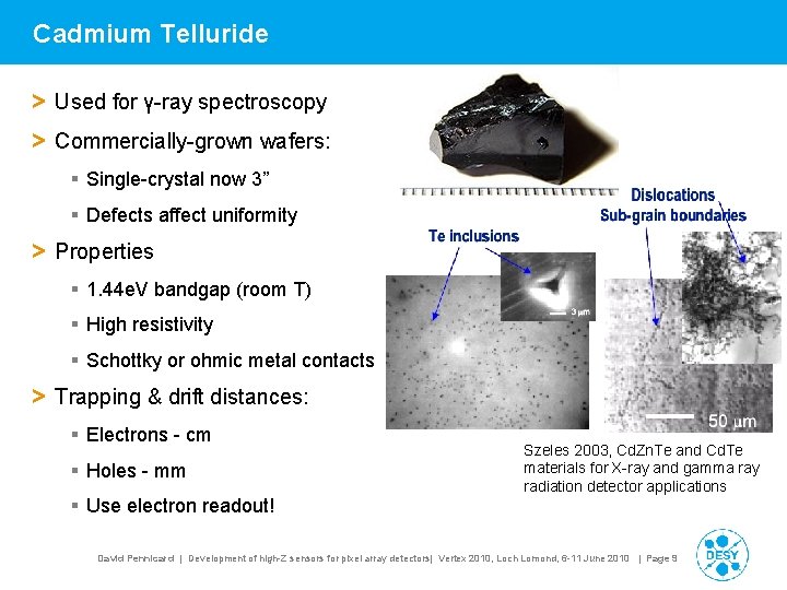
Cadmium Telluride > Used for γ-ray spectroscopy > Commercially-grown wafers: § Single-crystal now 3” § Defects affect uniformity > Properties § 1. 44 e. V bandgap (room T) § High resistivity § Schottky or ohmic metal contacts > Trapping & drift distances: § Electrons - cm § Holes - mm § Use electron readout! Szeles 2003, Cd. Zn. Te and Cd. Te materials for X-ray and gamma ray radiation detector applications David Pennicard | Development of high-Z sensors for pixel array detectors| Vertex 2010, Loch Lomond, 6 -11 June 2010 | Page 9

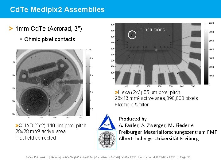
Cd. Te Medipix 2 Assemblies > 1 mm Cd. Te (Acrorad, 3”) Te inclusions § Ohmic pixel contacts >Hexa (2 x 3) 55 µm pixel pitch 28 x 43 mm 2 active area, 390, 000 pixels Flat field & filter >QUAD (2 x 2) 110 µm pixel pitch 28 x 28 mm 2 active area Flat field corrected Produced by A. Fauler, A. Zwerger, M. Fiederle Freiburger Materialforschungszentrum FMF Albert-Ludwigs-Universität Freiburg David Pennicard | Development of high-Z sensors for pixel array detectors| Vertex 2010, Loch Lomond, 6 -11 June 2010 | Page 10

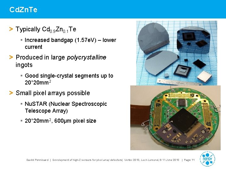
Cd. Zn. Te > Typically Cd 0. 9 Zn 0. 1 Te § Increased bandgap (1. 57 e. V) – lower current > Produced in large polycrystalline ingots § Good single-crystal segments up to 20*20 mm 2 > Small pixel arrays possible § Nu. STAR (Nuclear Spectroscopic Telescope Array) § 20*20 mm 2, 600μm pixel size David Pennicard | Development of high-Z sensors for pixel array detectors| Vertex 2010, Loch Lomond, 6 -11 June 2010 | Page 11

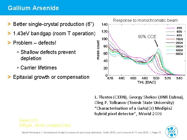
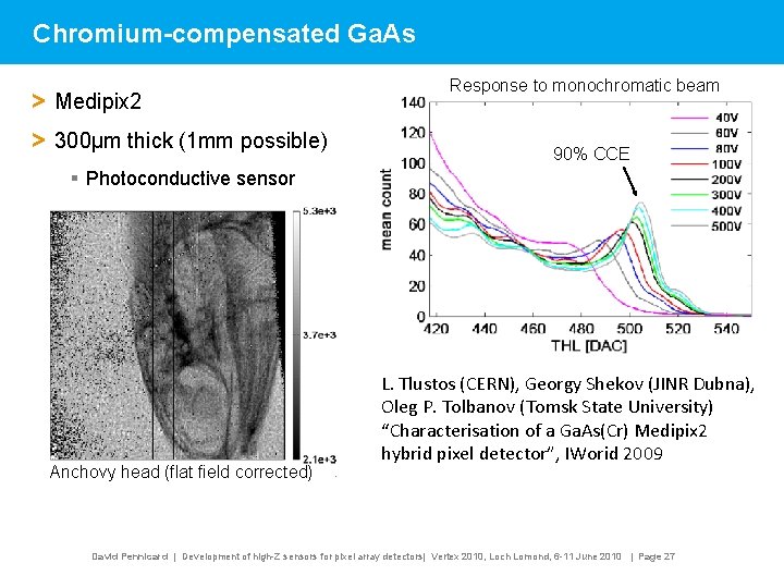
Gallium Arsenide Response to monochromatic beam > Better single-crystal production (6”) > 1. 43 e. V bandgap (room T operation) > Problem – defects! 90% CCE § Shallow defects prevent depletion § Carrier lifetimes > Epitaxial growth or compensation L. Tlustos (CERN), Georgy Shekov (JINR Dubna), Oleg P. Tolbanov (Tomsk State University) “Characterisation of a Ga. As(Cr) Medipix 2 hybrid pixel detector”, IWorid 2009 Ga. As (Cr) 300µm, ohmic contacts (Au) David Pennicard | Development of high-Z sensors for pixel array detectors| Vertex 2010, Loch Lomond, 6 -11 June 2010 | Page 12

Development of high-Z sensors for pixel array detectors > Applications of high-Z pixel arrays > Overview of high-Z sensors § Cd. Te / CZT § Ga. As > Work on pixellated Ge sensors at DESY > Summary David Pennicard | Development of high-Z sensors for pixel array detectors| Vertex 2010, Loch Lomond, 6 -11 June 2010 | Page 13

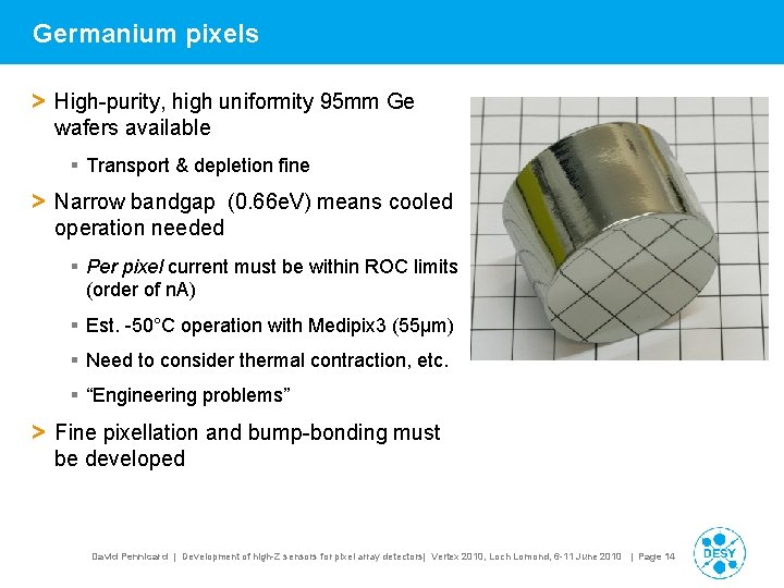
Germanium pixels > High-purity, high uniformity 95 mm Ge wafers available § Transport & depletion fine > Narrow bandgap (0. 66 e. V) means cooled operation needed § Per pixel current must be within ROC limits (order of n. A) § Est. -50°C operation with Medipix 3 (55µm) § Need to consider thermal contraction, etc. § “Engineering problems” > Fine pixellation and bump-bonding must be developed David Pennicard | Development of high-Z sensors for pixel array detectors| Vertex 2010, Loch Lomond, 6 -11 June 2010 | Page 14

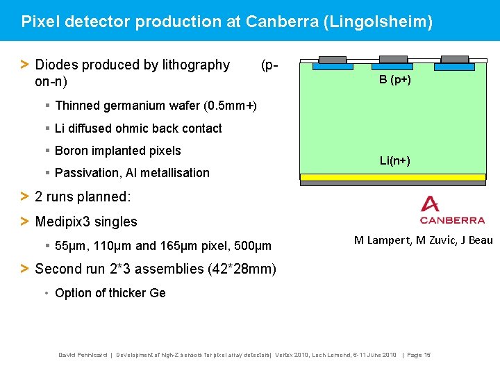
Pixel detector production at Canberra (Lingolsheim) > Diodes produced by lithography on-n) (p. B (p+) § Thinned germanium wafer (0. 5 mm+) § Li diffused ohmic back contact § Boron implanted pixels § Passivation, Al metallisation Li(n+) > 2 runs planned: > Medipix 3 singles § 55µm, 110µm and 165µm pixel, 500µm M Lampert, M Zuvic, J Beau > Second run 2*3 assemblies (42*28 mm) • Option of thicker Ge David Pennicard | Development of high-Z sensors for pixel array detectors| Vertex 2010, Loch Lomond, 6 -11 June 2010 | Page 15

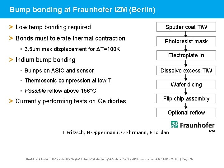
Bump bonding at Fraunhofer IZM (Berlin) > Low temp bonding required Sputter coat Ti. W > Bonds must tolerate thermal contraction Photoresist mask § 3. 5μm max displacement for ΔT=100 K > Indium bump bonding § Bumps on ASIC and sensor Electroplate In Dissolve excess Ti. W § Thermosonic compression at low T Wafer dicing § Possible reflow above 156°C > Currently performing tests on Ge diodes Flip chip assembly Optional reflow T Fritzsch, H Oppermann, O Ehrmann, R Jordan David Pennicard | Development of high-Z sensors for pixel array detectors| Vertex 2010, Loch Lomond, 6 -11 June 2010 | Page 16

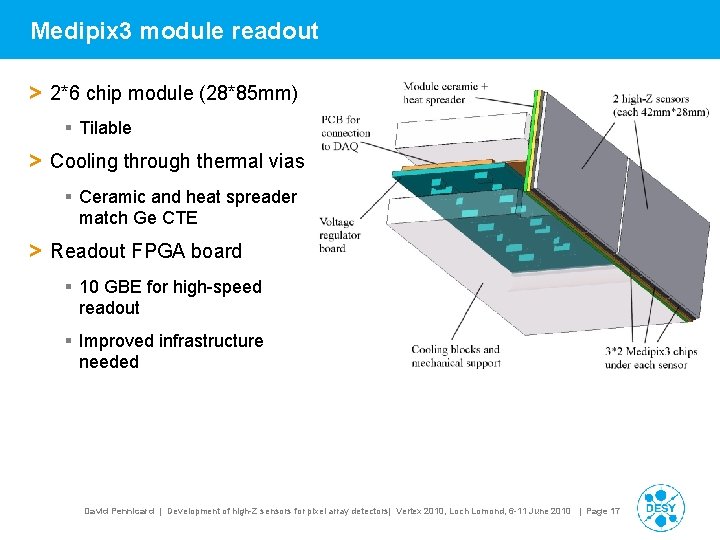
Medipix 3 module readout > 2*6 chip module (28*85 mm) § Tilable > Cooling through thermal vias § Ceramic and heat spreader match Ge CTE > Readout FPGA board § 10 GBE for high-speed readout § Improved infrastructure needed David Pennicard | Development of high-Z sensors for pixel array detectors| Vertex 2010, Loch Lomond, 6 -11 June 2010 | Page 17

Conclusions > Demand for high-Z hybrid pixels § Material science, biology / medicine, astronomy. . . > Promising results from Cd. Te / CZT, Ga. As § Commercial Cd. Te / CZT wafers improving § Improved Ga. As compensation > Ge pixels could provide high-uniformity sensors (albeit without room-temp operation) David Pennicard | Development of high-Z sensors for pixel array detectors| Vertex 2010, Loch Lomond, 6 -11 June 2010 | Page 18

Thanks for listening David Pennicard | Development of high-Z sensors for pixel array detectors| Vertex 2010, Loch Lomond, 6 -11 June 2010 | Page 19

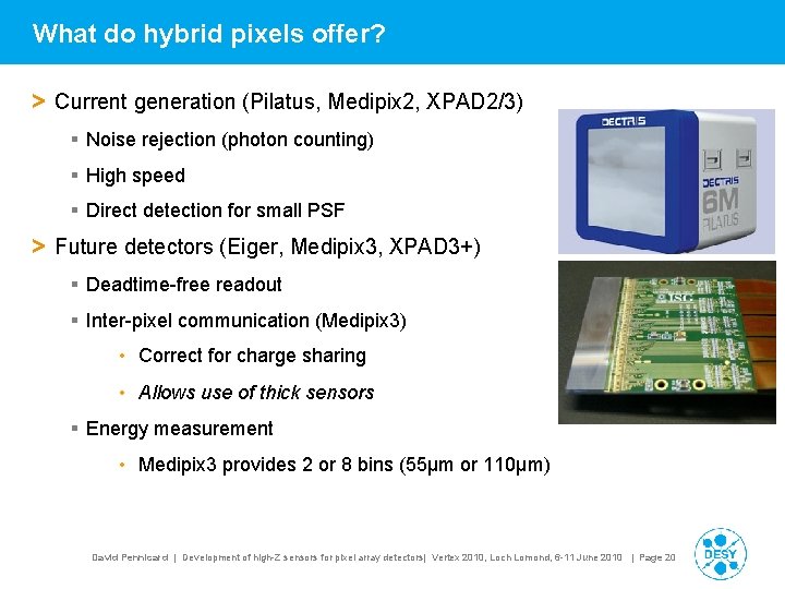
What do hybrid pixels offer? > Current generation (Pilatus, Medipix 2, XPAD 2/3) § Noise rejection (photon counting) § High speed § Direct detection for small PSF > Future detectors (Eiger, Medipix 3, XPAD 3+) § Deadtime-free readout § Inter-pixel communication (Medipix 3) • Correct for charge sharing • Allows use of thick sensors § Energy measurement • Medipix 3 provides 2 or 8 bins (55μm or 110μm) David Pennicard | Development of high-Z sensors for pixel array detectors| Vertex 2010, Loch Lomond, 6 -11 June 2010 | Page 20

Choice of material and fluorescence effects > Fluorescence harms performance immediately above k-shell § ~26. 7 ke. V for Cd. Te § ~11. 1 ke. V for Ge > Motivation to use different materials 35 ke. V photon in Cd. Te γ eγ e- 23. 2 ke. V fluorescence e. Ejected Cd kshell electron with 11. 8 ke. V 23. 2 ke. V deposited in other pixel David Pennicard | Development of high-Z sensors for pixel array detectors| Vertex 2010, Loch Lomond, 6 -11 June 2010 | Page 21

Choice of material and fluorescence effects > Fluorescence harms performance immediately above k-shell § ~26. 7 ke. V for Cd. Te § ~11. 1 ke. V for Ge > Motivation to use different materials 35 ke. V photon in Cd. Te γ eγ e- 23. 2 ke. V fluorescence e. Ejected Cd kshell electron with 11. 8 ke. V 23. 2 ke. V deposited in other pixel David Pennicard | Development of high-Z sensors for pixel array detectors| Vertex 2010, Loch Lomond, 6 -11 June 2010 | Page 22

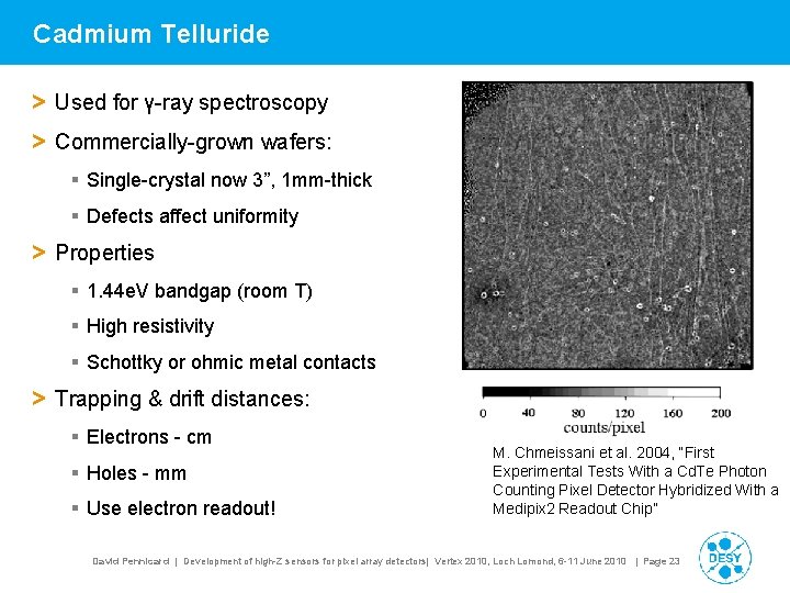
Cadmium Telluride > Used for γ-ray spectroscopy > Commercially-grown wafers: § Single-crystal now 3”, 1 mm-thick § Defects affect uniformity > Properties § 1. 44 e. V bandgap (room T) § High resistivity § Schottky or ohmic metal contacts > Trapping & drift distances: § Electrons - cm § Holes - mm § Use electron readout! M. Chmeissani et al. 2004, “First Experimental Tests With a Cd. Te Photon Counting Pixel Detector Hybridized With a Medipix 2 Readout Chip” David Pennicard | Development of high-Z sensors for pixel array detectors| Vertex 2010, Loch Lomond, 6 -11 June 2010 | Page 23

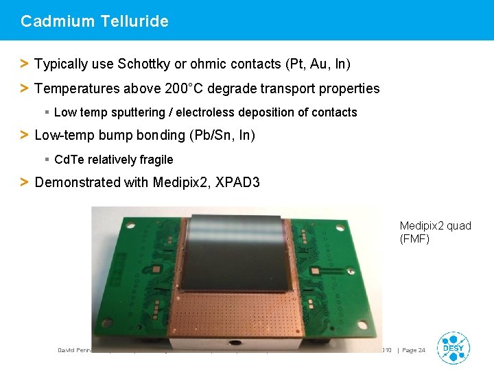
Cadmium Telluride > Typically use Schottky or ohmic contacts (Pt, Au, In) > Temperatures above 200°C degrade transport properties § Low temp sputtering / electroless deposition of contacts > Low-temp bump bonding (Pb/Sn, In) § Cd. Te relatively fragile > Demonstrated with Medipix 2, XPAD 3 Medipix 2 quad (FMF) David Pennicard | Development of high-Z sensors for pixel array detectors| Vertex 2010, Loch Lomond, 6 -11 June 2010 | Page 24

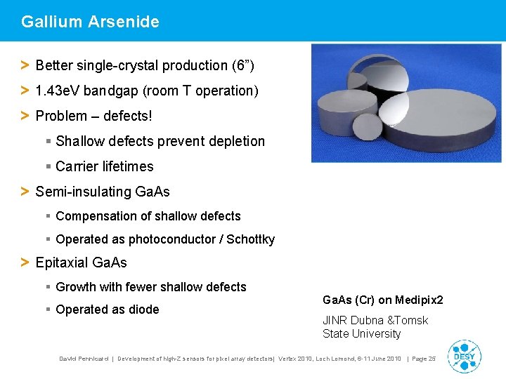
Gallium Arsenide > Better single-crystal production (6”) > 1. 43 e. V bandgap (room T operation) > Problem – defects! § Shallow defects prevent depletion § Carrier lifetimes > Semi-insulating Ga. As § Compensation of shallow defects § Operated as photoconductor / Schottky > Epitaxial Ga. As § Growth with fewer shallow defects § Operated as diode Ga. As (Cr) on Medipix 2 JINR Dubna &Tomsk State University David Pennicard | Development of high-Z sensors for pixel array detectors| Vertex 2010, Loch Lomond, 6 -11 June 2010 | Page 25

Gallium Arsenide – Semi insulating > As-rich growth produces deep defects (EL 2) § Compensate shallow traps § But increase electron trapping (~100μm) > Cr compensation promising § Dope n-type during growth, then overcompensate p-type with Cr diffusion > Metallised contacts § Au for photoconductor (right) § Pt-Ti-Au for Schottky > Moderate temp tolerance, physically fragile § Bonding at low temp § Indium / low T solder David Pennicard | Development of high-Z sensors for pixel array detectors| Vertex 2010, Loch Lomond, 6 -11 June 2010 | Page 26

Chromium-compensated Ga. As > Medipix 2 > 300μm thick (1 mm possible) Response to monochromatic beam 90% CCE § Photoconductive sensor Anchovy head (flat field corrected) L. Tlustos (CERN), Georgy Shekov (JINR Dubna), Oleg P. Tolbanov (Tomsk State University) “Characterisation of a Ga. As(Cr) Medipix 2 hybrid pixel detector”, IWorid 2009 David Pennicard | Development of high-Z sensors for pixel array detectors| Vertex 2010, Loch Lomond, 6 -11 June 2010 | Page 27

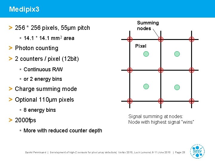
Medipix 3 > 256 * 256 pixels, 55µm pitch Summing nodes § 14. 1 * 14. 1 mm 2 area > Photon counting Pixel > 2 counters / pixel (12 bit) § Continuous R/W § or 2 energy bins > Charge summing mode > Optional 110µm pixels § 8 energy bins > 2000 fps Signal summing at nodes: Node with highest signal “wins” § More with reduced counter depth David Pennicard | Development of high-Z sensors for pixel array detectors| Vertex 2010, Loch Lomond, 6 -11 June 2010 | Page 29

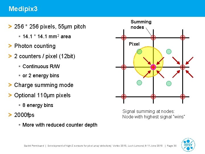
Medipix 3 > 256 * 256 pixels, 55µm pitch Summing nodes § 14. 1 * 14. 1 mm 2 area > Photon counting Pixel > 2 counters / pixel (12 bit) § Continuous R/W § or 2 energy bins > Charge summing mode > Optional 110µm pixels § 8 energy bins > 2000 fps Signal summing at nodes: Node with highest signal “wins” § More with reduced counter depth David Pennicard | Development of high-Z sensors for pixel array detectors| Vertex 2010, Loch Lomond, 6 -11 June 2010 | Page 30

Medipix 3 circuitry 2 counters allow continuous readwrite David Pennicard | Development of high-Z sensors for pixel array detectors| Vertex 2010, Loch Lomond, 6 -11 June 2010 | Page 31

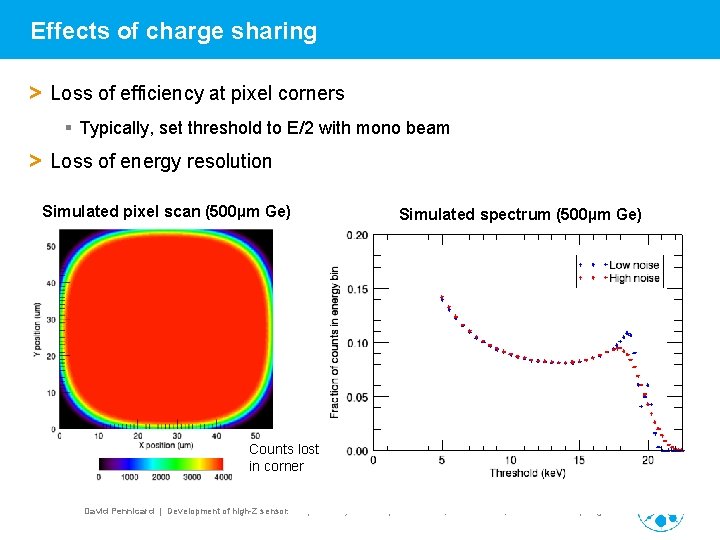
Effects of charge sharing > Loss of efficiency at pixel corners § Typically, set threshold to E/2 with mono beam > Loss of energy resolution Simulated pixel scan (500µm Ge) Simulated spectrum (500µm Ge) Counts lost in corner David Pennicard | Development of high-Z sensors for pixel array detectors| Vertex 2010, Loch Lomond, 6 -11 June 2010 | Page 32

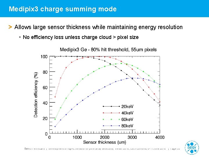
Medipix 3 charge summing mode > Allows large sensor thickness while maintaining energy resolution § No efficiency loss unless charge cloud > pixel size David Pennicard | Development of high-Z sensors for pixel array detectors| Vertex 2010, Loch Lomond, 6 -11 June 2010 | Page 33

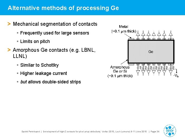
Alternative methods of processing Ge > Mechanical segmentation of contacts § Frequently used for large sensors § Limits on pitch > Amorphous Ge contacts (e. g. LBNL, LLNL) § Similar to Schottky § Higher leakage current § but allows double-sided strips David Pennicard | Development of high-Z sensors for pixel array detectors| Vertex 2010, Loch Lomond, 6 -11 June 2010 | Page 34