Development of a 3 D detector on a
,")


 Literature Simulation Relative permittivity 11. 8 -11. 9")


- Slides: 24
Development of a 3 D detector on a hydrogenated amorphous silicon substrate M. Menichelli(a), M. Boscardin(b)(c), M. Crivellari (c), J. Davis(f), S. Dunand(i) , L. Fanò(a)(d), A. Morozzi(a)(g), F. Moscatelli(a)(e), M. Movileanu-Ionica(a), D. Passeri(a)(g) , M. Petasecca(f), M. Piccini(a), A. Rossi(a)(d), A. Scorzoni(a)(g), G. Verzellesi(b)(h), N. Wyrsch(i). (a) INFN, Sez. di Perugia, Perugia (ITALY) (b) INFN TIPFA, Trento (ITALY) (c)Fondazione Bruno Kessler, Trento (ITALY) (d) Dip. Di Fisica dell’Università degli studi di Perugia, Perugia (ITALY) (e) CNR-IOM Perugia (ITALY) (f)Centre for Medical Radiation Physics, University of Wollongong, NSW 2522, (AUSTRALIA) (g)Dip. Di Ingegneria dell’Università degli studi di Perugia, Perugia (ITALY) (h) Università di Modena e Reggio Emilia, Modena (ITALY) (i) Ecole Polytechnique Federale de Lausanne (EPFL), Institute of Microengineering (IMT), Neuchatel, (SWITZERLAND)
Hydrogenated Amorphous Silicon a -Si: H �The first study on a-Si: H was reported by Chittik et al. in 1969 �Material was obtained by plasma-enhanced chemical vapor deposition (PECVD) of Si. H 4 (Silane) + Hydrogen. �Substantial progress of the a-Si: H technology were performed when Spear and Lecomber demonstrated that this material could be substitutionally doped (both in n and p-types); this led to the development of various types of electronic devices such as transistors, solar cells, memories and eventually, in the second half of the 80’, planar radiation detector in p-i-n structures.
A-Si: H Structure and density of states
A-Si: H planar detectors pros & cons I �Pros: �Extremely low radiation damage. �Low cost production (this technology is currently used in solar cells production) �Possible deposition in many different substrate materials
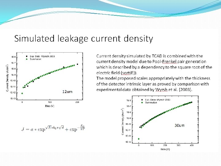
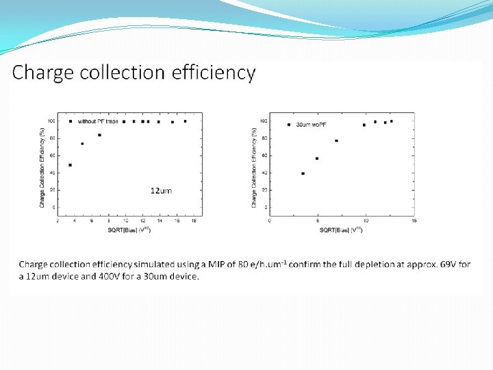
A-Si: H planar detectors pros & cons II �Cons �High depletion voltage (about 1100 V for 50 um thickness) �Growth on a non-removable substrate �Pretty low charge collection efficiency: 50%(on a 30 um thick detector) energy to create a e-h pair similar to crystalline silicon (3. 4 -4. 0 e. V) �High leakage current (in the order of few u. A/cm 2 on a 30 um detector) �Low mobility (from 1 to 10 cm 2 /Vs for electrons 2 orders of magnitude less for holes) �Limited thickness of substrates (max 100 -150 um)
Displacement damage on a 30 um a -Si: H planar detector
Signal formation on planar a-Si: H detectors
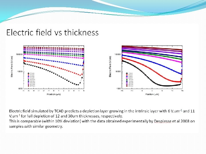
3 D technology on a-Si: H �The depletion potential applies on the interelectrode distance that is not coincident with the thickness of the detector �Never attempted before �Noise reduction test at cold temperature (e. g. -30°C)
Baseline 3 D detector structure
Possible 3 D detector configurations
Technological options for doping the electrodes �Option 1: Selective layers of metal oxide deposited via ALD �Option 2: Ion implantation and low temperature activation (250 °C or below )
Prototype development �Phase 1: construction of planar diodes with option 1 and 2 doping techniques. �Phase 2: Construction of basic 3 D structures in order to test the two proposed doping techniques. �Phase 3: Construction of 3 D detectors in various configurations.
Diodes and test structures layout in phase 1 prototypes �Before depositing a-Si: H the p-type silicon wafer is divided in two halves and in one of the two halves is oxidated. �In the non-oxidated half vertical diodes are fabricated �In oxidated half lateral diodes are fabricated
Vertical diodes
Lateral diodes
Final complete Layout
A-Si: H material simulation Parameter (units) Literature Simulation Relative permittivity 11. 8 -11. 9 11. 7 Electron mobility (cm 2 V− 1 s− 1) 0. 5 -20 10 Hole mobility (cm 2 V− 1 s− 1) 0. 003 -10 0. 01 Band Gap (e. V) 1. 7 -1. 9 1. 84 Dangling bond density (cm 3) 5 x 10¹⁴ – 5 x 10¹⁶ 4 x 10¹⁵ Activation energy (e. V) 0. 42 -0. 49 0. 52
Defects model
Timeline of the 3 years program �Tape out of the phase 1 prototype. DONE � Completion of production of the phase 1 prototype by January at most. �Testing of the phase 1 prototype and beginning of definition of the phase 2 prototype by april 2020 �Construction of phase 2 prototype by mid 2020. �Testing of phase 2 prototype and design of the phase 3 prototype by the end of 2020 �Production and testing of the phase 3 prototype by the end of 2021
The future of 3 D a-Si: H detector �Fabrication of an actual pixel detector bump-bonded on a readout chip. �Deposition of a-Si: H directly on the readout chip and construction of the 3 D detector on the deposited substrate.