Detailed Design Review Hybrid Audio Dynamics Processor Team
Detailed Design Review Hybrid Audio Dynamics Processor Team Lead: William Sender Jeffrey Auclair Bryan Beatrez Michael Ferry 1
Agenda ● Problem Definition ○ Problem Statement ○ Customer Requirements ○ Engineering Requirements ● System Design ○ Functional Decomposition ○ System Architecture 2
Agenda ● Detailed Design ○ Embedded Design ○ Hardware Design ○ Software Design ○ Auto-Mode ○ BOM ○ Risk Assessment ● MSD II Plan 3
Section One Problem Definition 4
Problem Statement • • Audio amplitude control for motion picture shows. Maintain the quality and dynamics of the sound. Improve flexibility while maintaining audio quality. Maintain usability that of previous devices. 5
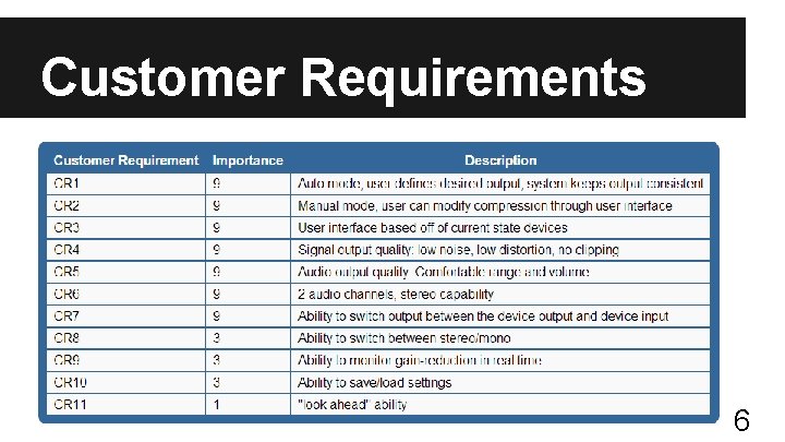
Customer Requirements 6
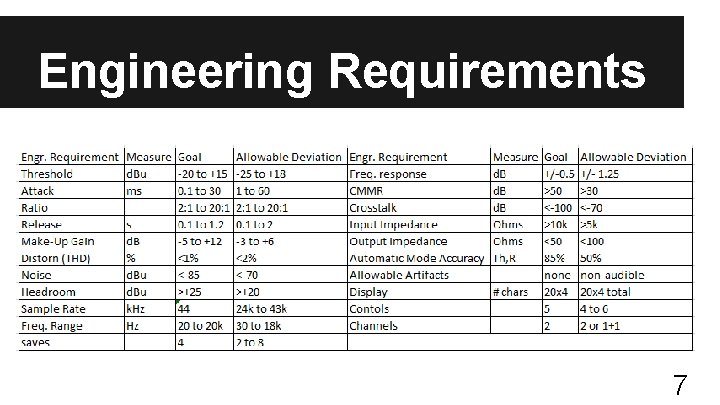
Engineering Requirements 7

Section Two System Design 8
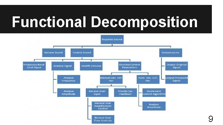
Functional Decomposition 9
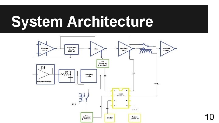
System Architecture 10
Section Three Detailed Design 11
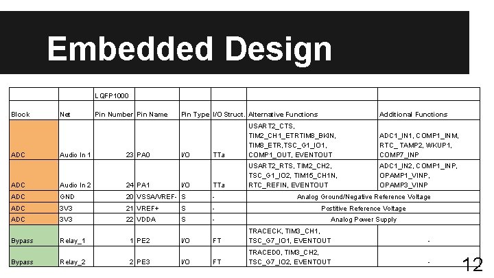
Embedded Design LQFP 1000 Block ADC Net Audio In 1 Pin Number Pin Name 23 PA 0 Pin Type I/O Struct. Alternative Functions I/O TTa USART 2_CTS, TIM 2_CH 1_ETRTIM 8_BKIN, TIM 8_ETR, TSC_G 1_IO 1, COMP 1_OUT, EVENTOUT ADC 1_IN 1, COMP 1_INM, RTC_ TAMP 2, WKUP 1, COMP 7_INP TTa USART 2_RTS, TIM 2_CH 2, TSC_G 1_IO 2, TIM 15_CH 1 N, RTC_REFIN, EVENTOUT ADC 1_IN 2, COMP 1_INP, OPAMP 1_VINP, OPAMP 3_VINP ADC Audio In 2 24 PA 1 ADC GND 20 VSSA/VREF- S - Analog Ground/Negative Reference Voltage ADC 3 V 3 21 VREF+ S - Postitive Reference Voltage ADC 3 V 3 22 VDDA S - Analog Power Supply Bypass Relay_1 I/O FT TRACECK, TIM 3_CH 1, TSC_G 7_IO 1, EVENTOUT - FT TRACED 0, TIM 3_CH 2, TSC_G 7_IO 2, EVENTOUT - Bypass Relay_2 1 PE 2 2 PE 3 I/O Additional Functions I/O 12
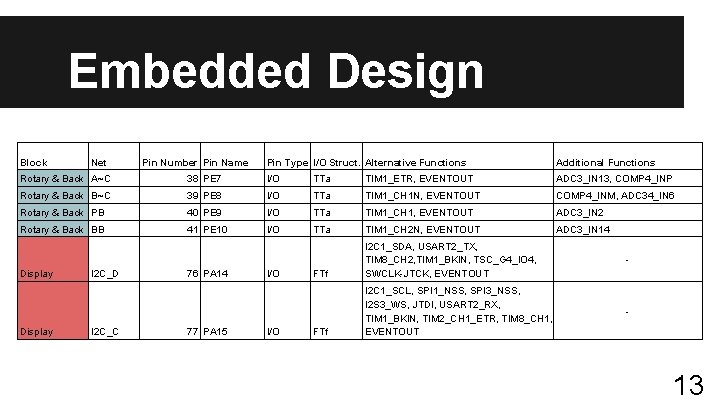
Embedded Design Block Net Pin Number Pin Name Pin Type I/O Struct. Alternative Functions Additional Functions Rotary & Back A~C 38 PE 7 I/O TTa TIM 1_ETR, EVENTOUT ADC 3_IN 13, COMP 4_INP Rotary & Back B~C 39 PE 8 I/O TTa TIM 1_CH 1 N, EVENTOUT COMP 4_INM, ADC 34_IN 6 Rotary & Back PB 40 PE 9 I/O TTa TIM 1_CH 1, EVENTOUT ADC 3_IN 2 Rotary & Back BB 41 PE 10 I/O TTa TIM 1_CH 2 N, EVENTOUT ADC 3_IN 14 - FTf I 2 C 1_SDA, USART 2_TX, TIM 8_CH 2, TIM 1_BKIN, TSC_G 4_IO 4, SWCLK-JTCK, EVENTOUT - FTf I 2 C 1_SCL, SPI 1_NSS, SPI 3_NSS, I 2 S 3_WS, JTDI, USART 2_RX, TIM 1_BKIN, TIM 2_CH 1_ETR, TIM 8_CH 1, EVENTOUT Display I 2 C_D I 2 C_C 76 PA 14 77 PA 15 I/O 13
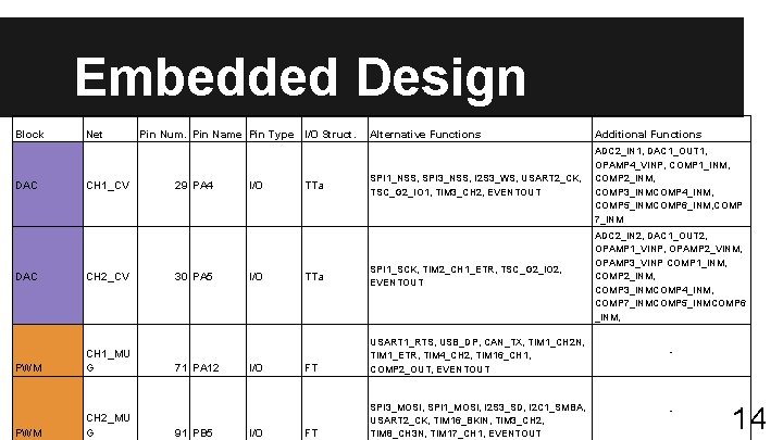
Embedded Design Block DAC Net CH 1_CV DAC CH 2_CV PWM CH 1_MU G PWM CH 2_MU G Pin Num. Pin Name Pin Type I/O Struct. 29 PA 4 30 PA 5 71 PA 12 91 PB 5 I/O I/O TTa Alternative Functions Additional Functions SPI 1_NSS, SPI 3_NSS, I 2 S 3_WS, USART 2_CK, TSC_G 2_IO 1, TIM 3_CH 2, EVENTOUT ADC 2_IN 1, DAC 1_OUT 1, OPAMP 4_VINP, COMP 1_INM, COMP 2_INM, COMP 3_INMCOMP 4_INM, COMP 5_INMCOMP 6_INM, COMP 7_INM SPI 1_SCK, TIM 2_CH 1_ETR, TSC_G 2_IO 2, EVENTOUT ADC 2_IN 2, DAC 1_OUT 2, OPAMP 1_VINP, OPAMP 2_VINM, OPAMP 3_VINP COMP 1_INM, COMP 2_INM, COMP 3_INMCOMP 4_INM, COMP 7_INMCOMP 5_INMCOMP 6 _INM, FT USART 1_RTS, USB_DP, CAN_TX, TIM 1_CH 2 N, TIM 1_ETR, TIM 4_CH 2, TIM 16_CH 1, COMP 2_OUT, EVENTOUT FT SPI 3_MOSI, SPI 1_MOSI, I 2 S 3_SD, I 2 C 1_SMBA, USART 2_CK, TIM 16_BKIN, TIM 3_CH 2, TIM 8_CH 3 N, TIM 17_CH 1, EVENTOUT - - 14
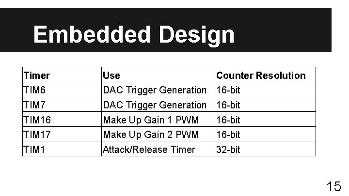
Embedded Design Timer Use Counter Resolution TIM 6 DAC Trigger Generation 16 -bit TIM 7 DAC Trigger Generation 16 -bit TIM 16 Make Up Gain 1 PWM 16 -bit TIM 17 Make Up Gain 2 PWM 16 -bit TIM 1 Attack/Release Timer 32 -bit 15
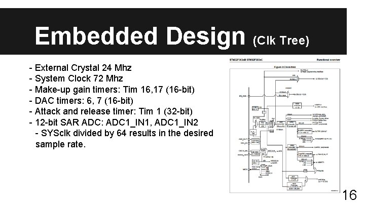
Embedded Design (Clk Tree) - External Crystal 24 Mhz - System Clock 72 Mhz - Make-up gain timers: Tim 16, 17 (16 -bit) - DAC timers: 6, 7 (16 -bit) - Attack and release timer: Tim 1 (32 -bit) - 12 -bit SAR ADC: ADC 1_IN 1, ADC 1_IN 2 - SYSclk divided by 64 results in the desired sample rate. 16
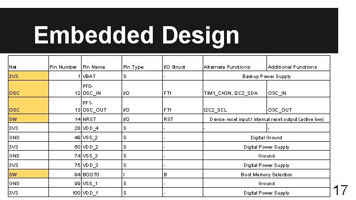
Embedded Design Net Pin Number Pin Name Pin Type I/O Struct S - Alternate Functions Additional Functions 3 V 3 1 VBAT Backup Power Supply OSC PF 012 OSC_IN I/O FTf TIM 1_CH 3 N, I 2 C 2_SDA OSC_IN OSC PF 113 OSC_OUT I/O FTf I 2 C 2_SCL OSC_OUT SW 14 NRST I/O RST 3 V 3 28 VDD_4 S - GND 49 VSS_2 S - Digital Ground 3 V 3 50 VDD_2 S - Digital Power Supply GND 74 VSS_3 S - Ground 3 V 3 75 VDD_3 S - Digital Power Supply SW 94 BOOT 0 I B Boot Memory Selection GND 99 VSS_1 S - Ground 3 V 3 100 VDD_1 S - Digital Power Supply Device reset input / internal reset output (active low) - - 17
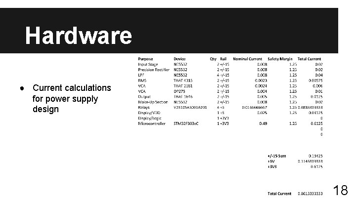
Hardware ● Current calculations for power supply design 18

Hardware 19
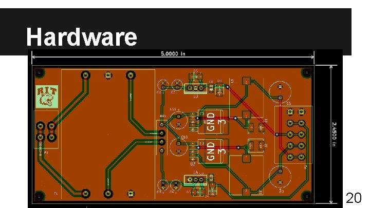
Hardware 20
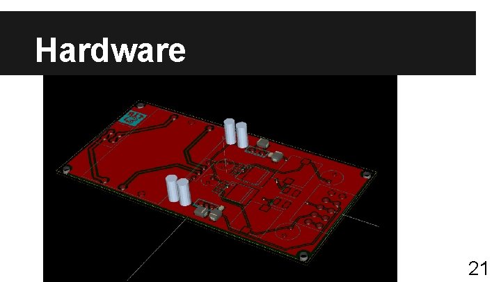
Hardware 21
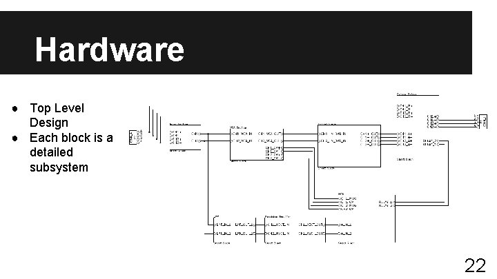
Hardware ● Top Level Design ● Each block is a detailed subsystem 22
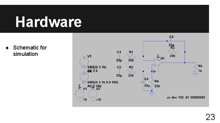
Hardware ● Schematic for simulation 23
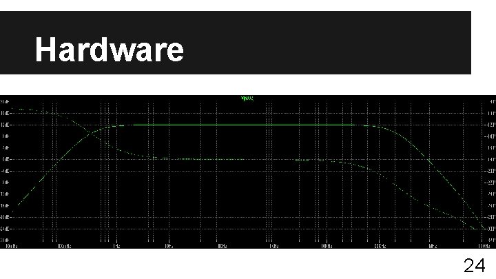
Hardware 24
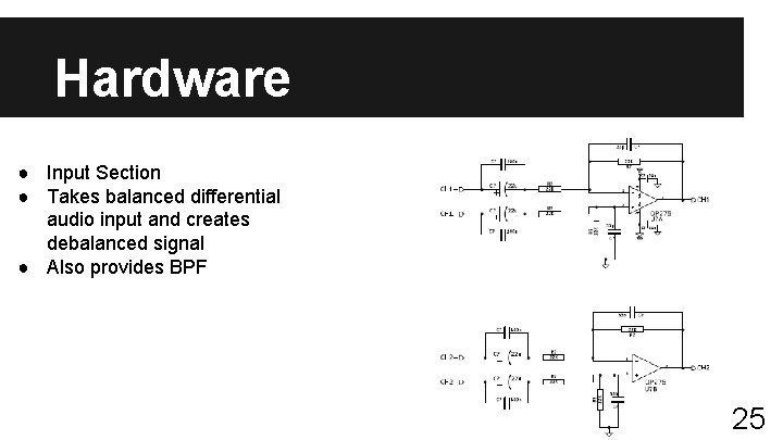
Hardware ● Input Section ● Takes balanced differential audio input and creates debalanced signal ● Also provides BPF 25
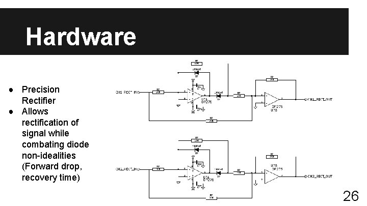
Hardware ● Precision Rectifier ● Allows rectification of signal while combating diode non-idealities (Forward drop, recovery time) 26
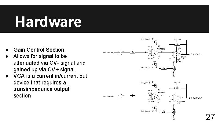
Hardware ● Gain Control Section ● Allows for signal to be attenuated via CV- signal and gained up via CV+ signal. ● VCA is a current in/current out device that requires a transimpedance output section 27
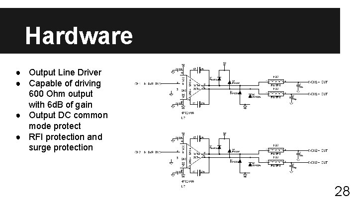
Hardware ● Output Line Driver ● Capable of driving 600 Ohm output with 6 d. B of gain ● Output DC common mode protect ● RFI protection and surge protection 28
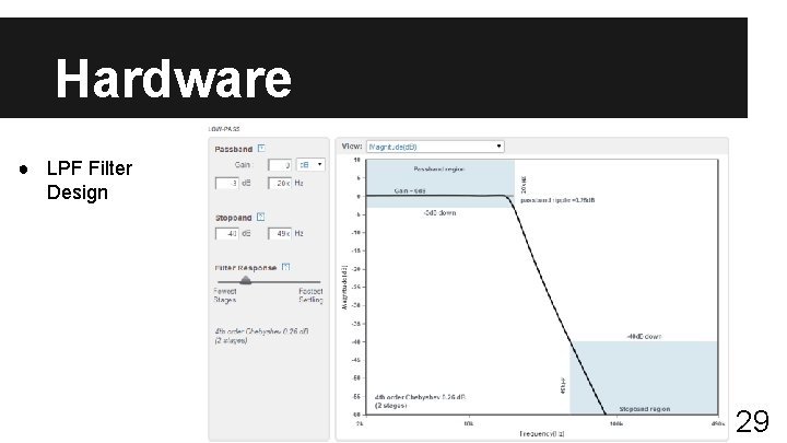
Hardware ● LPF Filter Design 29
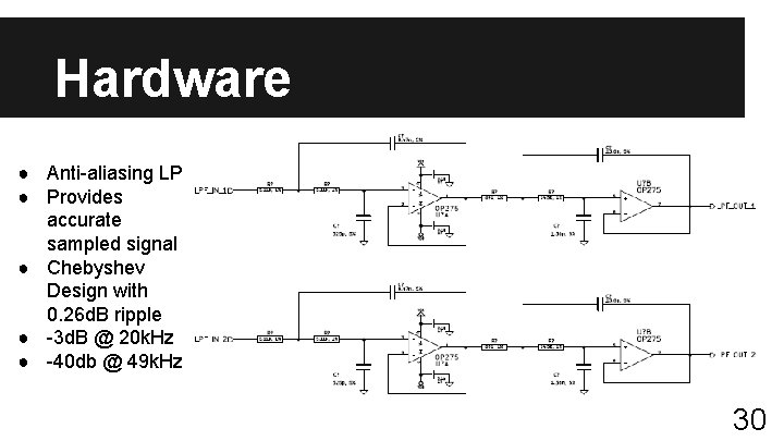
Hardware ● Anti-aliasing LPF ● Provides accurate sampled signal ● Chebyshev Design with 0. 26 d. B ripple ● -3 d. B @ 20 k. Hz ● -40 db @ 49 k. Hz 30
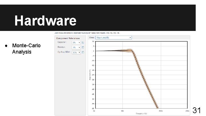
Hardware ● Monte-Carlo Analysis 31
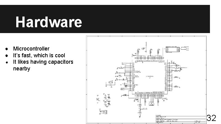
Hardware ● Microcontroller ● It’s fast, which is cool ● It likes having capacitors nearby 32

Hardware ● Takes 3. 3 V signals from the microcontroller and converts them to 5 V. ● Same in either direction. 33
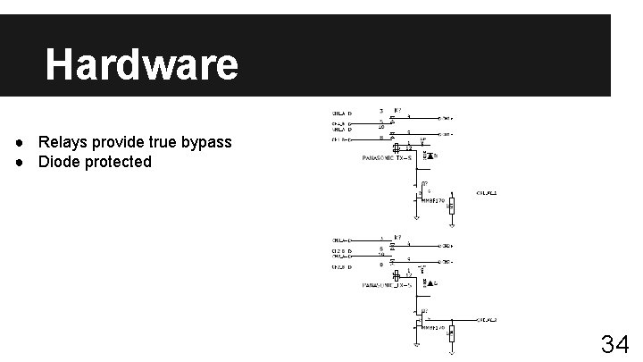
Hardware ● Relays provide true bypass ● Diode protected 34

Software Top-Level 35
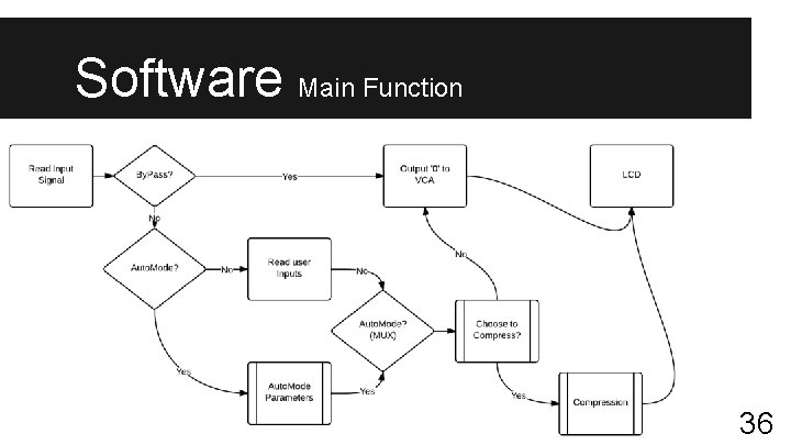
Software Main Function 36
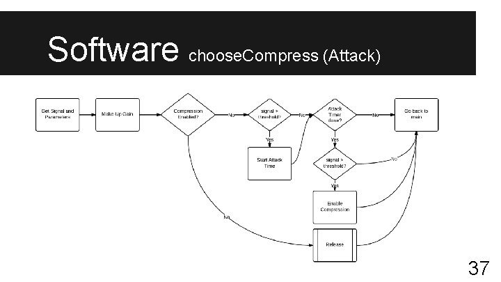
Software choose. Compress (Attack) 37
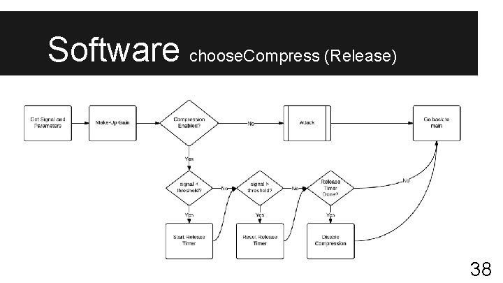
Software choose. Compress (Release) 38
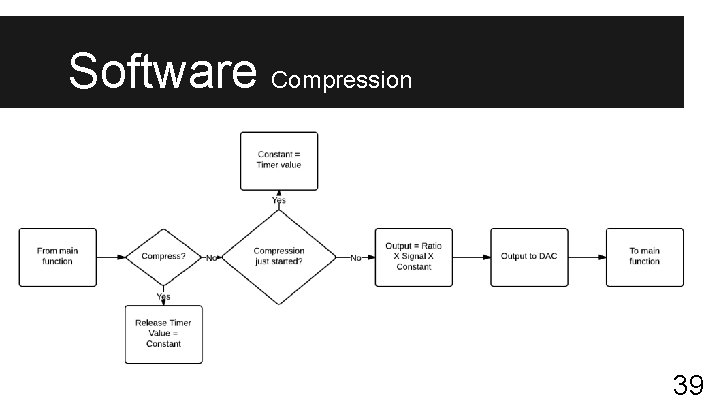
Software Compression 39
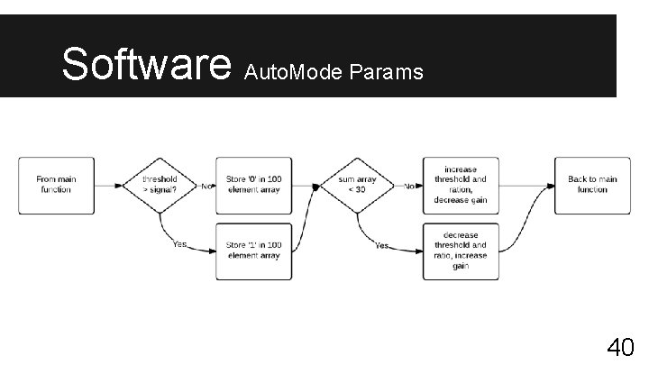
Software Auto. Mode Params 40
Software Pseudo Code Break from powerpoint to show pseudo code 41
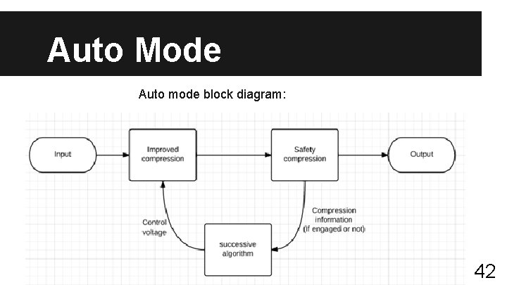
Auto Mode Auto mode block diagram: 42
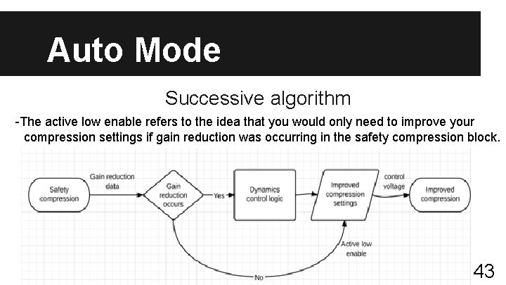
Auto Mode Successive algorithm -The active low enable refers to the idea that you would only need to improve your compression settings if gain reduction was occurring in the safety compression block. 43
Auto Mode Safety Mode - When auto mode is initialized this all the signal conditioning that occurs. - Safety mode is a limiter to the incoming signal, +3 dbu threshold 20: 1 ratio. - It also helps balance the system by feeding back compression data. 44
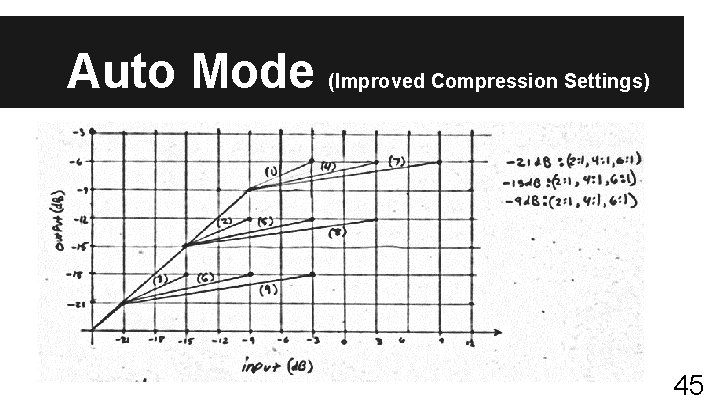
Auto Mode (Improved Compression Settings) 45
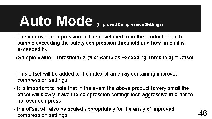
Auto Mode (Improved Compression Settings) - The improved compression will be developed from the product of each sample exceeding the safety compression threshold and how much it is exceeded by. (Sample Value - Threshold) X (# of Samples Exceeding Threshold) = Offset - This offset will be added to the index of an array containing improved compression settings. - It is important to note that in the event the above product is very small the offset will slowly make the compression settings less aggressive in order to not over compress. - the offset will also be scaled appropriately for the array of improved compression settings. 46
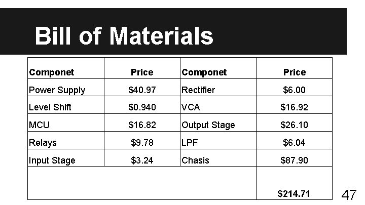
Bill of Materials Componet Price Power Supply $40. 97 Rectifier $6. 00 Level Shift $0. 940 VCA $16. 92 MCU $16. 82 Output Stage $26. 10 Relays $9. 78 LPF $6. 04 Input Stage $3. 24 Chasis $87. 90 $214. 71 47
Bill of Materials Break from powerpoint to show full Bill of Materials 48
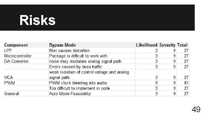
Risks 49
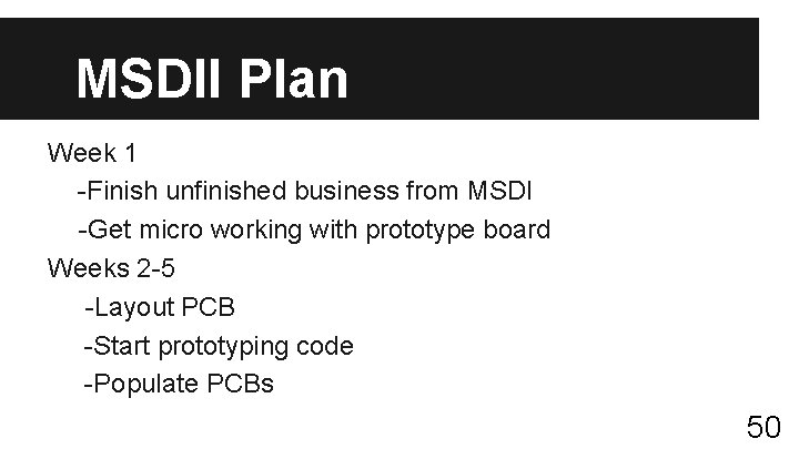
MSDII Plan Week 1 -Finish unfinished business from MSDI -Get micro working with prototype board Weeks 2 -5 -Layout PCB -Start prototyping code -Populate PCBs 50
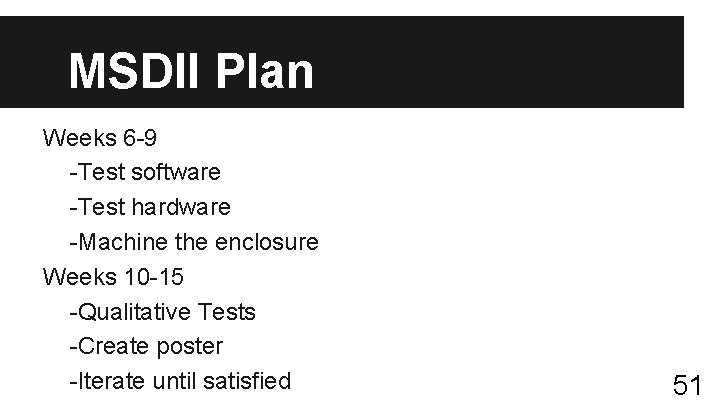
MSDII Plan Weeks 6 -9 -Test software -Test hardware -Machine the enclosure Weeks 10 -15 -Qualitative Tests -Create poster -Iterate until satisfied 51

Questions ? 52
- Slides: 52