DET 2183 Analogue Electronics CHAPTER 1 Lecture I
- Slides: 16

DET 218/3 Analogue Electronics CHAPTER 1 Lecture I Introduction to BJT Amplifier

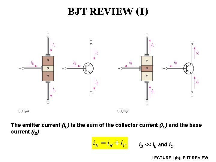
BJT REVIEW (I) The emitter current (i. E) is the sum of the collector current (i. C) and the base current (i. B) i. B << i. E and i. C LECTURE I (b): BJT REVIEW

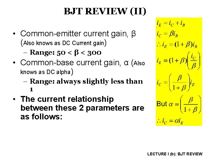
BJT REVIEW (II) • Common-emitter current gain, β (Also knows as DC Current gain) – Range: 50 < β < 300 • Common-base current gain, α (Also knows as DC alpha) – Range: always slightly less than 1 • The current relationship between these 2 parameters are as follows: LECTURE I (b): BJT REVIEW

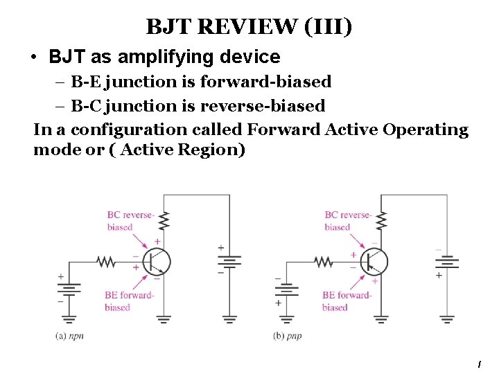
BJT REVIEW (III) • BJT as amplifying device – B-E junction is forward-biased – B-C junction is reverse-biased In a configuration called Forward Active Operating mode or ( Active Region) LECTURE I (b): BJT REVIEW

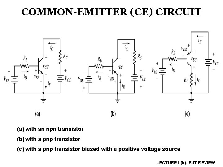
COMMON-EMITTER (CE) CIRCUIT (a) with an npn transistor (b) with a pnp transistor (c) with a pnp transistor biased with a positive voltage source LECTURE I (b): BJT REVIEW

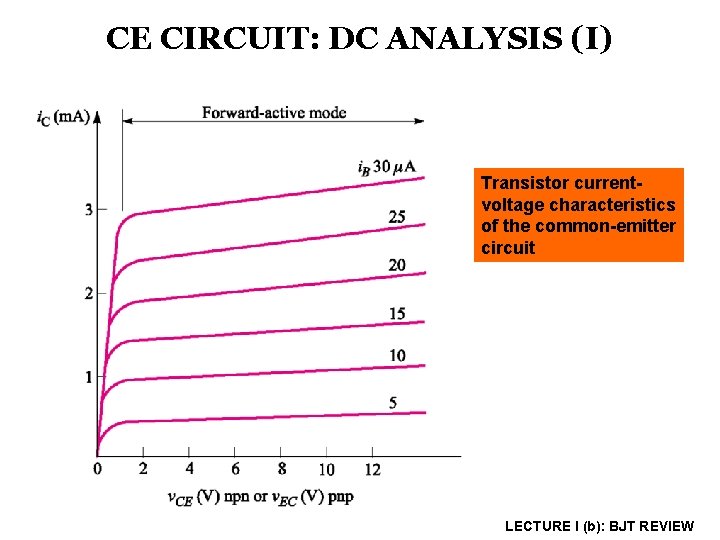
CE CIRCUIT: DC ANALYSIS (I) Transistor currentvoltage characteristics of the common-emitter circuit LECTURE I (b): BJT REVIEW

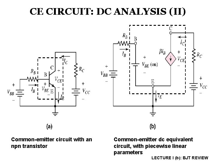
CE CIRCUIT: DC ANALYSIS (II) Common-emitter circuit with an npn transistor Common-emitter dc equivalent circuit, with piecewise linear parameters LECTURE I (b): BJT REVIEW

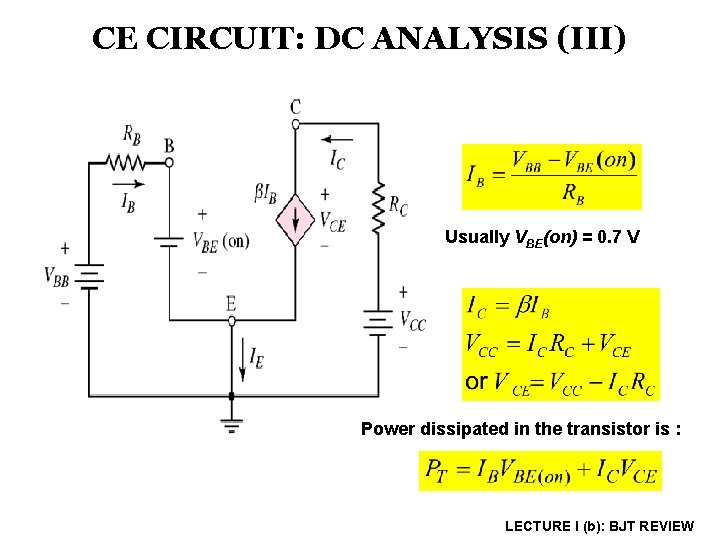
CE CIRCUIT: DC ANALYSIS (III) Usually VBE(on) = 0. 7 V Power dissipated in the transistor is : LECTURE I (b): BJT REVIEW

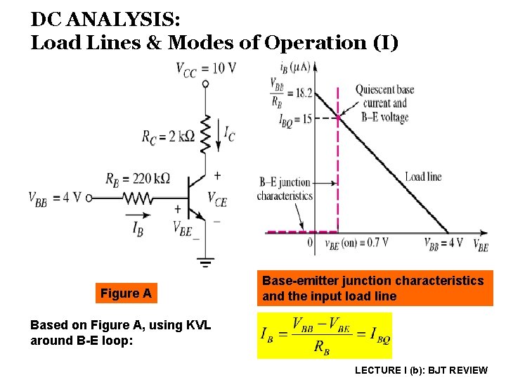
DC ANALYSIS: Load Lines & Modes of Operation (I) Figure A Base-emitter junction characteristics and the input load line Based on Figure A, using KVL around B-E loop: LECTURE I (b): BJT REVIEW

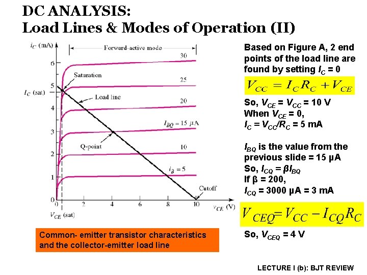
DC ANALYSIS: Load Lines & Modes of Operation (II) Based on Figure A, 2 end points of the load line are found by setting IC = 0 So, VCE = VCC = 10 V When VCE = 0, IC = VCC/RC = 5 m. A IBQ is the value from the previous slide = 15 µA So, ICQ = βIBQ If β = 200, ICQ = 3000 µA = 3 m. A Common- emitter transistor characteristics and the collector-emitter load line So, VCEQ = 4 V LECTURE I (b): BJT REVIEW

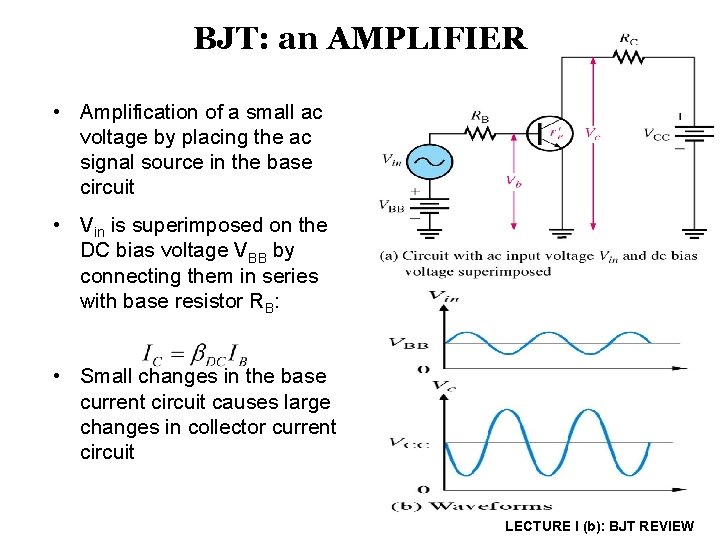
BJT: an AMPLIFIER • Amplification of a small ac voltage by placing the ac signal source in the base circuit • Vin is superimposed on the DC bias voltage VBB by connecting them in series with base resistor RB: • Small changes in the base current circuit causes large changes in collector current circuit LECTURE I (b): BJT REVIEW

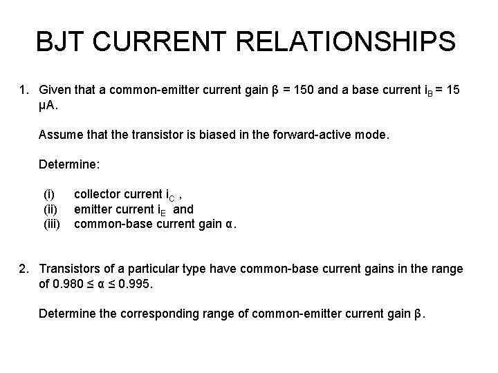
BJT CURRENT RELATIONSHIPS 1. Given that a common-emitter current gain β = 150 and a base current i. B = 15 µA. Assume that the transistor is biased in the forward-active mode. Determine: (i) (iii) collector current i. C , emitter current i. E and common-base current gain α. 2. Transistors of a particular type have common-base current gains in the range of 0. 980 ≤ α ≤ 0. 995. Determine the corresponding range of common-emitter current gain β.

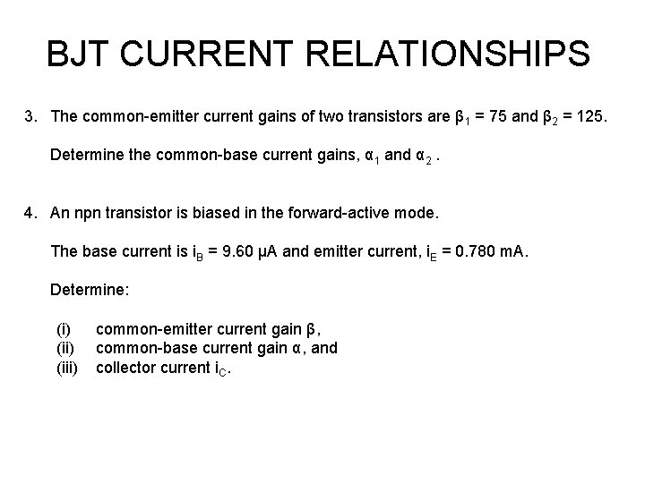
BJT CURRENT RELATIONSHIPS 3. The common-emitter current gains of two transistors are β 1 = 75 and β 2 = 125. Determine the common-base current gains, α 1 and α 2. 4. An npn transistor is biased in the forward-active mode. The base current is i. B = 9. 60 µA and emitter current, i. E = 0. 780 m. A. Determine: (i) (iii) common-emitter current gain β, common-base current gain α, and collector current i. C.

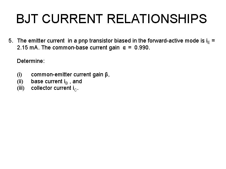
BJT CURRENT RELATIONSHIPS 5. The emitter current in a pnp transistor biased in the forward-active mode is i. E = 2. 15 m. A. The common-base current gain α = 0. 990. Determine: (i) (iii) common-emitter current gain β, base current i. B , and collector current i. C.

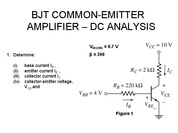
BJT COMMON-EMITTER AMPLIFIER – DC ANALYSIS VBE(ON) = 0. 7 V 1. Determine: (i) (iii) (iv) β = 200 base current IB , emitter current IE , collector current IC collector-emitter voltage, VCE and Figure 1

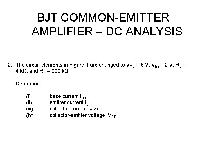
BJT COMMON-EMITTER AMPLIFIER – DC ANALYSIS 2. The circuit elements in Figure 1 are changed to VCC = 5 V, VBB = 2 V, RC = 4 kΩ, and RB = 200 kΩ Determine: (i) (iii) (iv) base current IB , emitter current IE , collector current IC and collector-emitter voltage, VCE