Designing with MAXPLUS II Copyright 1997 Altera Corporation



- Slides: 119

Designing with MAX+PLUS II Copyright © 1997 Altera Corporation

Class Agenda n MAX+PLUS II Design Environment n MAX+PLUS II Design Methodology – – – Design Entry Compilation Simulation Timing Analysis Device Programming n Review and Support Copyright © 1997 Altera Corporation

MAX+PLUS II Design Environment Copyright © 1997 Altera Corporation

MAX+PLUS II IS. . . n A fully integrated CPLD development system – Provides an architecture-independent design environment • Supports ALL Altera devices (one Library for all devices) – Supports broad range of design needs • Design Entry • Synthesis • Place & Route (fitting) • Simulation • Timing Analysis • Device Programming – Provides extensive on-line help – Supports multiple platforms ( PC, Workstation ) – Supports multiple EDA vendors and standards Copyright © 1997 Altera Corporation

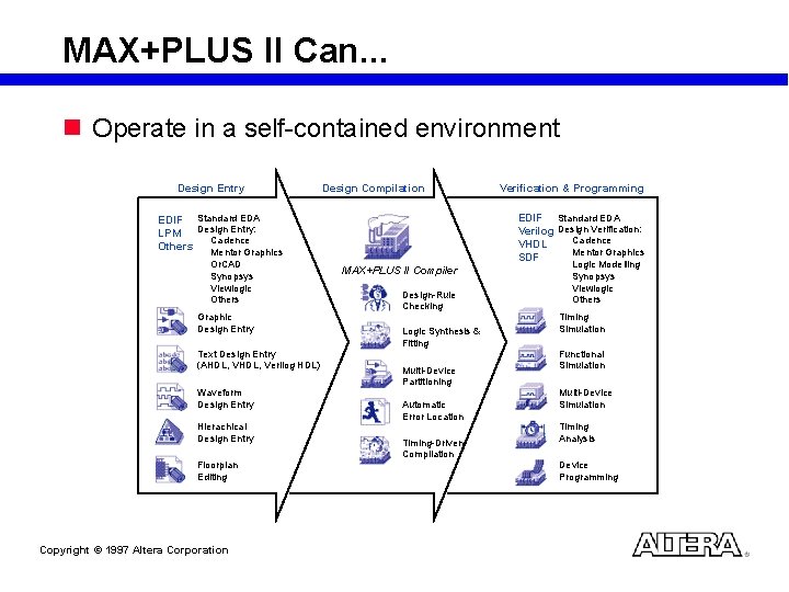
MAX+PLUS II Can. . . n Operate in a self-contained environment Design Entry Design Compilation EDIF Standard EDA Verilog Design Verification: Cadence VHDL Mentor Graphics SDF EDIF Standard EDA LPM Design Entry: Cadence Others Mentor Graphics Or. CAD Synopsys Viewlogic Others Graphic Design Entry Text Design Entry (AHDL, Verilog HDL) Waveform Design Entry Hierachical Design Entry Floorplan Editing Copyright © 1997 Altera Corporation Verification & Programming MAX+PLUS II Compiler Design-Rule Checking Logic Synthesis & Fitting Multi-Device Partitioning Automatic Error Location Timing-Driven Compilation Logic Modelling Synopsys Viewlogic Others Timing Simulation Functional Simulation Multi-Device Simulation Timing Analysis Device Programming

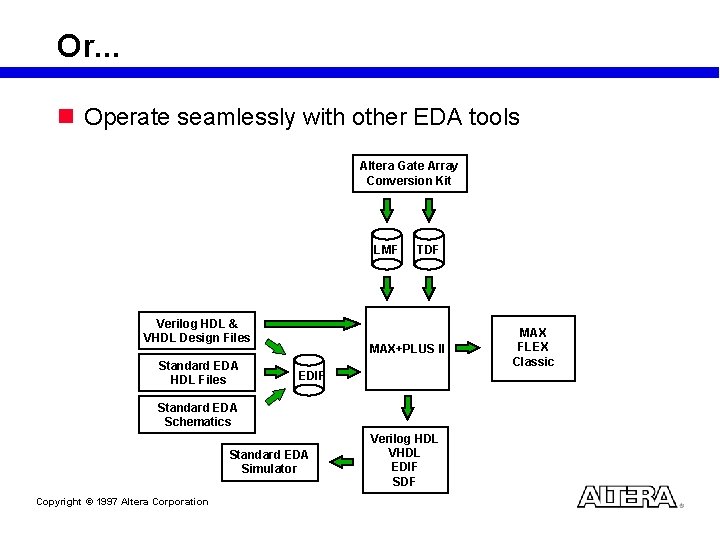
Or. . . n Operate seamlessly with other EDA tools Altera Gate Array Conversion Kit LMF Verilog HDL & VHDL Design Files Standard EDA HDL Files TDF MAX+PLUS II EDIF Standard EDA Schematics Standard EDA Simulator Copyright © 1997 Altera Corporation Verilog HDL VHDL EDIF SDF MAX FLEX Classic

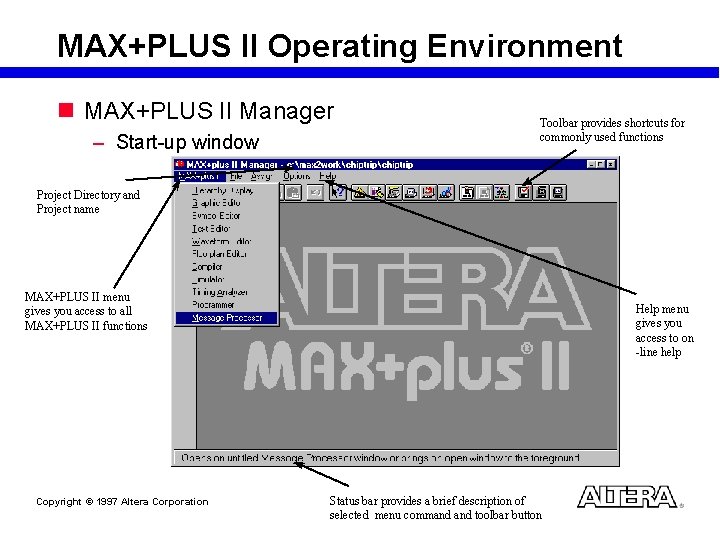
MAX+PLUS II Operating Environment n MAX+PLUS II Manager – Start-up window Toolbar provides shortcuts for commonly used functions Project Directory and Project name MAX+PLUS II menu gives you access to all MAX+PLUS II functions Copyright © 1997 Altera Corporation Help menu gives you access to on -line help Status bar provides a brief description of selected menu command toolbar button

Questions about MAX+PLUS II? n MAX+PLUS II On-Line Help has the answers – Contains the complete up-to-date information on MAX+PLUS II – Provides tips on how to effectively work with MAX+PLUS II tools – Provides answers and examples n Digital Library CD-ROM Copyright © 1997 Altera Corporation

MAX+PLUS II Design Methodology Copyright © 1997 Altera Corporation

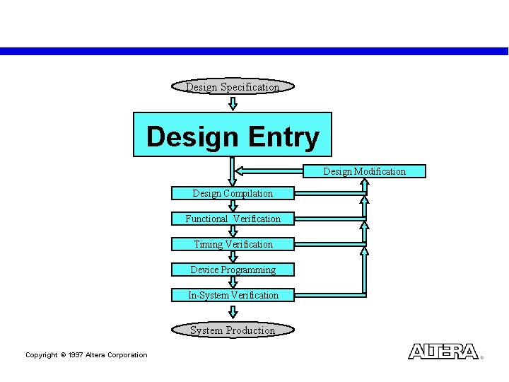
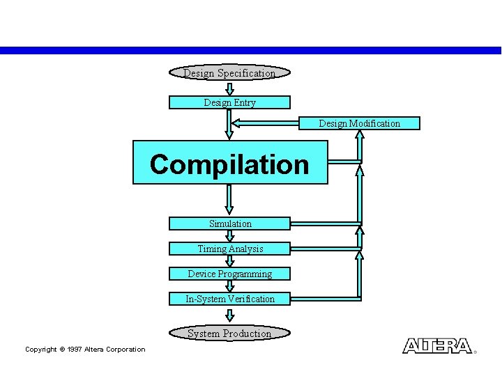
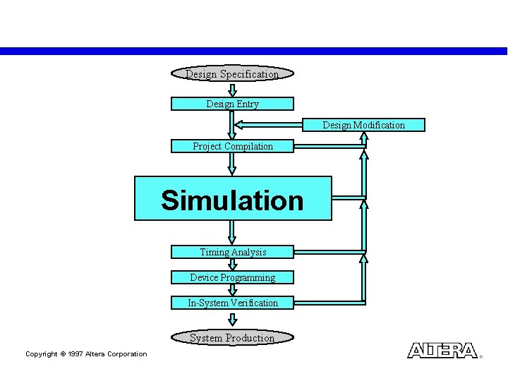
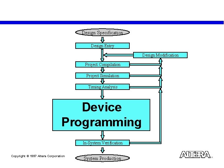
Design Specification Design Entry Design Modification Design Compilation Functional Verification Timing Verification Device Programming In-System Verification System Production Copyright © 1997 Altera Corporation

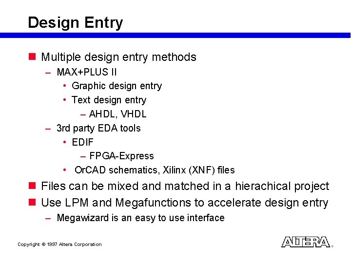
Design Entry n Multiple design entry methods – MAX+PLUS II • Graphic design entry • Text design entry – AHDL, VHDL – 3 rd party EDA tools • EDIF – FPGA-Express • Or. CAD schematics, Xilinx (XNF) files n Files can be mixed and matched in a hierachical project n Use LPM and Megafunctions to accelerate design entry – Megawizard is an easy to use interface Copyright © 1997 Altera Corporation

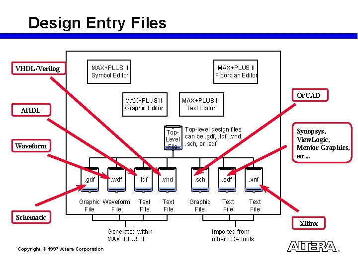
Design Entry Files VHDL/Verilog MAX+PLUS II Symbol Editor MAX+PLUS II Floorplan Editor MAX+PLUS II Graphic Editor AHDL Or. CAD MAX+PLUS II Text Editor Top-level design files Level can be. gdf, . tdf, . vhd, File. sch, or. edf Waveform . gdf . wdf Graphic Waveform File Synopsys, View. Logic, Mentor Graphics, etc. . tdf . vhd . sch . edf . xnf Text File Graphic File Text File Schematic Xilinx Generated within MAX+PLUS II Copyright © 1997 Altera Corporation Imported from other EDA tools

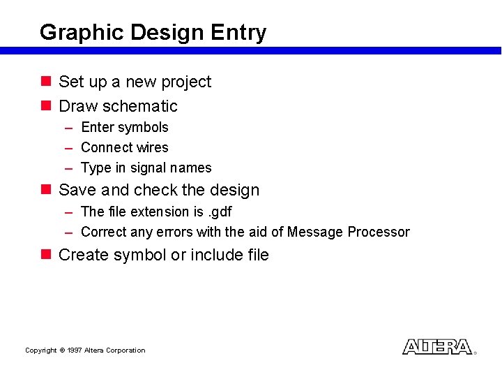
Graphic Design Entry n Set up a new project n Draw schematic – Enter symbols – Connect wires – Type in signal names n Save and check the design – The file extension is. gdf – Correct any errors with the aid of Message Processor n Create symbol or include file Copyright © 1997 Altera Corporation

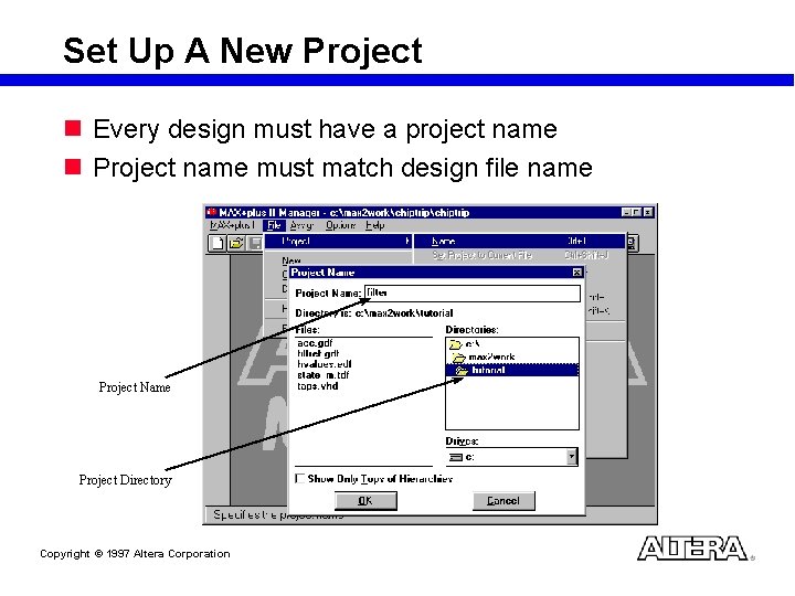
Set Up A New Project n Every design must have a project name n Project name must match design file name Project Name Project Directory Copyright © 1997 Altera Corporation

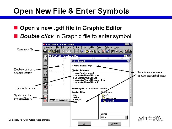
Open New File & Enter Symbols n Open a new. gdf file in Graphic Editor n Double click in Graphic file to enter symbol Open new file Double click in Graphic Editor Symbol libraries Symbols in the selected library Copyright © 1997 Altera Corporation Type in symbol name or click on symbol name

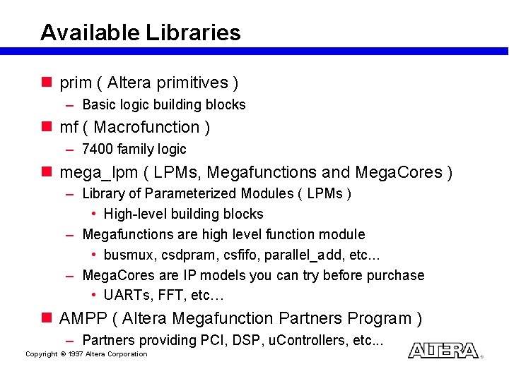
Available Libraries n prim ( Altera primitives ) – Basic logic building blocks n mf ( Macrofunction ) – 7400 family logic n mega_lpm ( LPMs, Megafunctions and Mega. Cores ) – Library of Parameterized Modules ( LPMs ) • High-level building blocks – Megafunctions are high level function module • busmux, csdpram, csfifo, parallel_add, etc. . . – Mega. Cores are IP models you can try before purchase • UARTs, FFT, etc… n AMPP ( Altera Megafunction Partners Program ) – Partners providing PCI, DSP, u. Controllers, etc. . . Copyright © 1997 Altera Corporation

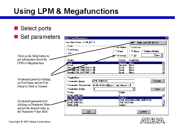
Using LPM & Megafunctions n Select ports n Set parameters Click on the Help button to get information about the LPM or Megafunction Set desired ports by clicking on Port Name and set Port Status to Used or Unused Set desired parameters by clicking on Parameter Name and set the desired value in the Parameter Value field Copyright © 1997 Altera Corporation

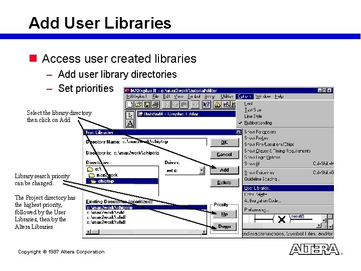
Add User Libraries n Access user created libraries – Add user library directories – Set priorities Select the library directory then click on Add Library search priority can be changed. The Project directory has the highest priority, followed by the User Libraries, then by the Altera Libraries Copyright © 1997 Altera Corporation

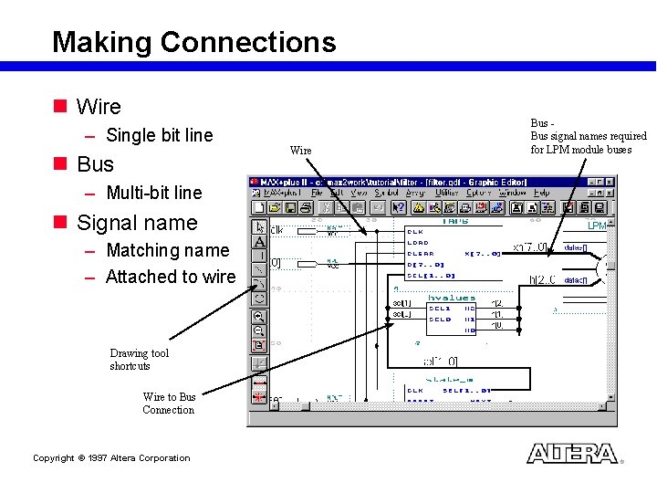
Making Connections n Wire – Single bit line n Bus – Multi-bit line n Signal name – Matching name – Attached to wire Drawing tool shortcuts Wire to Bus Connection Copyright © 1997 Altera Corporation Wire Bus signal names required for LPM module buses

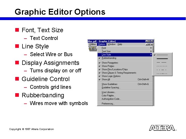
Graphic Editor Options n Font, Text Size – Text Control n Line Style – Select Wire or Bus n Display Assignments – Turns display on or off n Guideline Control – Controls grid lines n Rubberbanding – Wires move with symbols Copyright © 1997 Altera Corporation

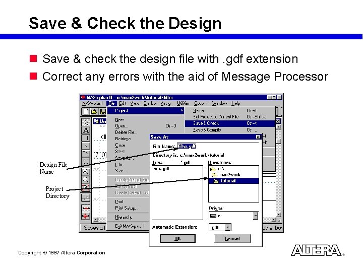
Save & Check the Design n Save & check the design file with. gdf extension n Correct any errors with the aid of Message Processor Design File Name Project Directory Copyright © 1997 Altera Corporation

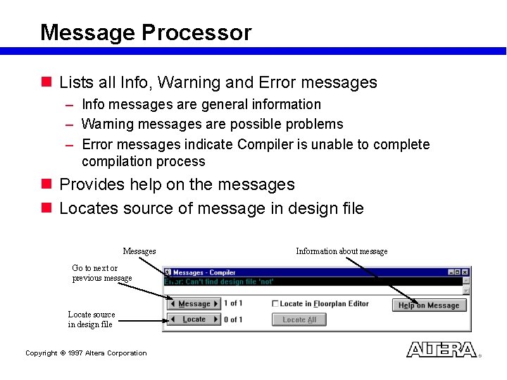
Message Processor n Lists all Info, Warning and Error messages – Info messages are general information – Warning messages are possible problems – Error messages indicate Compiler is unable to complete compilation process n Provides help on the messages n Locates source of message in design file Messages Go to next or previous message Locate source in design file Copyright © 1997 Altera Corporation Information about message

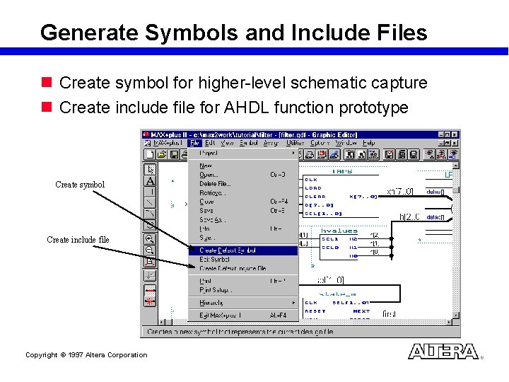
Generate Symbols and Include Files n Create symbol for higher-level schematic capture n Create include file for AHDL function prototype Create symbol Create include file Copyright © 1997 Altera Corporation

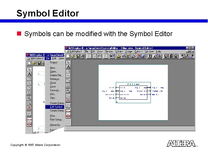
Symbol Editor n Symbols can be modified with the Symbol Editor Copyright © 1997 Altera Corporation

Example Section (LAB 1) Copyright © 1997 Altera Corporation

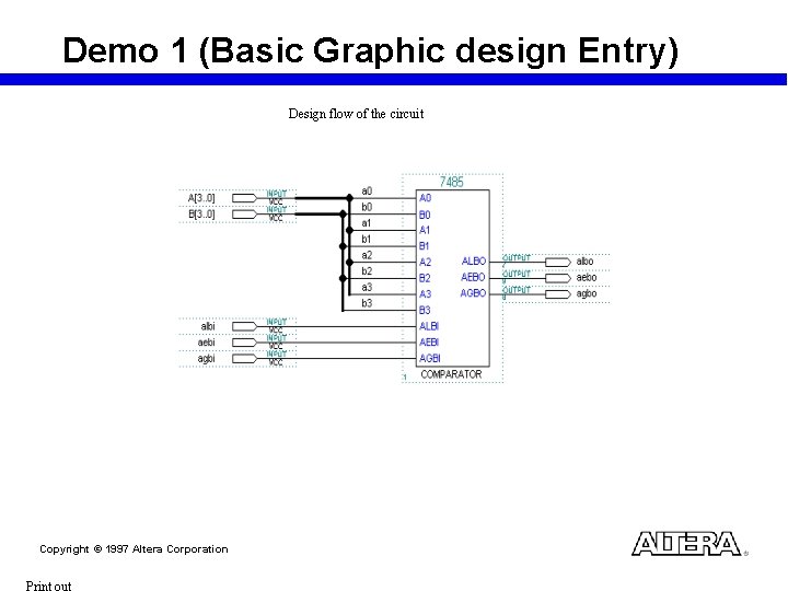
Demo 1 (Basic Graphic design Entry) Design flow of the circuit Copyright © 1997 Altera Corporation

Demo 2 (1) Draw the following circuit (2) Use the Save & Check Option (3) Use the Error Message to Locate the Error (4) Correct the Error Copyright © 1997 Altera Corporation

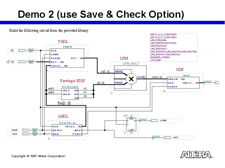
Demo 2 (use Save & Check Option) Build the following circuit from the provided library VHDL LPM GDF Viewlogic EDIF Sel[1. . 0] AHDL Copyright © 1997 Altera Corporation

Text Design Entry n Set up a new project – Same as Graphic Design Entry n Enter text description – AHDL – VHDL n Save & check the design – Similar to Graphic Design Entry – The file extension is. tdf or. vhd Copyright © 1997 Altera Corporation

AHDL n Altera Hardware Description Language n High-level hardware behavior description language n Uses Boolean equations, arithmetic operators, truth tables, conditional statements, etc. n Especially well-suited for large or complex state machines n All described behavior is implemented concurrently n Use Insert AHDL Template in the Text Editor Learn more about AHDL in the customer training class: Designing with MAX+plus II Using AHDL Copyright © 1997 Altera Corporation

VHDL n n n VHSIC Hardware Description Language IEEE standard High-level hardware behavior description language Especially well-suited for large or complex designs Use Insert VHDL Template in the Text Editor Learn more about VHDL in the customer training class: Designing with MAX+plus II Using VHDL Copyright © 1997 Altera Corporation

Imported Design n Top-level Design – Some top-level designs can be read directly by the compiler • EDIF Netlist files • VHDL Netlist files • Xilinx Netlist files – Save top-level Or. CAD schematics as. gdf file in Graphic Editor n Subdesigns (lower level modules) – EDIF, VHDL, Or. CAD schematics, Xilinx files • Create symbols and include files • Embed symbols or include files in Graphic or Text Editor – Other proprietary files • JEDEC, ABEL, PALASM • Conversion ultilities exist in Altera ftp site Copyright © 1997 Altera Corporation

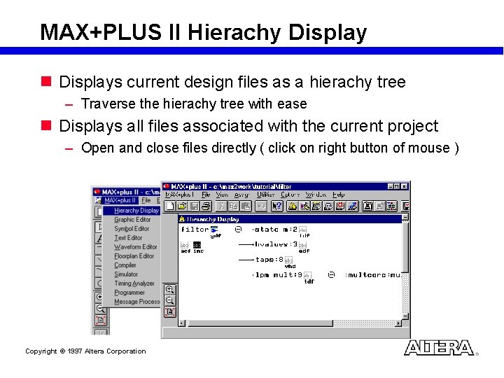
MAX+PLUS II Hierachy Display n Displays current design files as a hierachy tree – Traverse the hierachy tree with ease n Displays all files associated with the current project – Open and close files directly ( click on right button of mouse ) Copyright © 1997 Altera Corporation

Design Entry Recommendations n Use LPM/Megafunction whenever possible n Use hierarachical design methodology n Use Hierarachy Display for fast access to design file at any level n Use Message Processor to locate source of error in design file Copyright © 1997 Altera Corporation

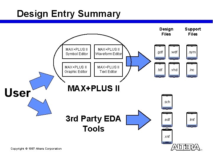
Design Entry Summary Design Files User Support Files MAX+PLUS II Symbol Editor MAX+PLUS II Waveform Editor . gdf . wdf . sym MAX+PLUS II Graphic Editor MAX+PLUS II Text Editor . tdf . vhd . inc MAX+PLUS II. sch 3 rd Party EDA Tools . edf . xnf Copyright © 1997 Altera Corporation . lmf

Design Specification Design Entry Design Modification Compilation Simulation Timing Analysis Device Programming In-System Verification System Production Copyright © 1997 Altera Corporation

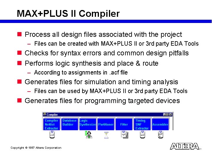
MAX+PLUS II Compiler n Process all design files associated with the project – Files can be created with MAX+PLUS II or 3 rd party EDA Tools n Checks for syntax errors and common design pitfalls n Performs logic synthesis and place & route – According to assignments in. acf file n Generates files for simulation and timing analysis – Files can be used by MAX+PLUS II or 3 rd party EDA Tools n Generates files for programming targeted devices Copyright © 1997 Altera Corporation

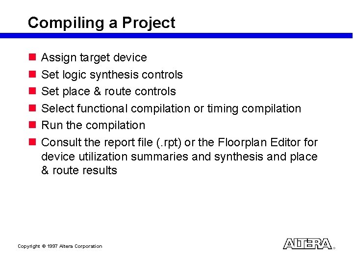
Compiling a Project n n n Assign target device Set logic synthesis controls Set place & route controls Select functional compilation or timing compilation Run the compilation Consult the report file (. rpt) or the Floorplan Editor for device utilization summaries and synthesis and place & route results Copyright © 1997 Altera Corporation

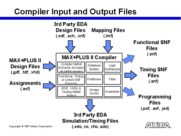
Compiler Input and Output Files 3 rd Party EDA Design Files Mapping Files (. edf, . sch, . xnf) (. lmf) Functional SNF Files MAX+PLUS II Design Files MAX+PLUS II Compiler (. gdf, . tdf, . vhd) Compiler Netlist Extractor (includes all netlist readers Database Builder Logic Synthesizer Assignments Functional, Timing, or Linked SNF Extractor Partitioner Fitter EDIF, VHDL & Verilog Netlist Writers Design Doctor Assembler (. acf) (. snf) Timing SNF Files (. snf) Programming Files (. pof, . sof, . jed) 3 rd Party EDA Simulation/Timing Files Copyright © 1997 Altera Corporation (. edo, vho, sdo)

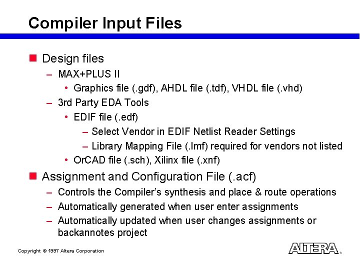
Compiler Input Files n Design files – MAX+PLUS II • Graphics file (. gdf), AHDL file (. tdf), VHDL file (. vhd) – 3 rd Party EDA Tools • EDIF file (. edf) – Select Vendor in EDIF Netlist Reader Settings – Library Mapping File (. lmf) required for vendors not listed • Or. CAD file (. sch), Xilinx file (. xnf) n Assignment and Configuration File (. acf) – Controls the Compiler’s synthesis and place & route operations – Automatically generated when user enter assignments – Automatically updated when user changes assignments or backannotes project Copyright © 1997 Altera Corporation

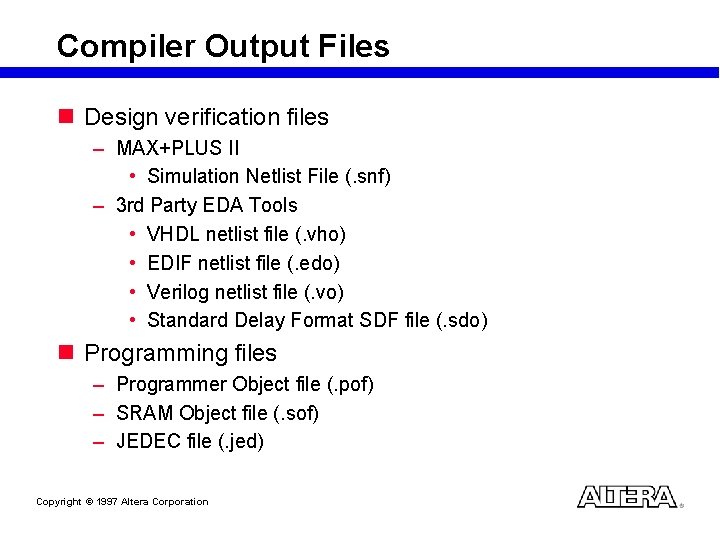
Compiler Output Files n Design verification files – MAX+PLUS II • Simulation Netlist File (. snf) – 3 rd Party EDA Tools • VHDL netlist file (. vho) • EDIF netlist file (. edo) • Verilog netlist file (. vo) • Standard Delay Format SDF file (. sdo) n Programming files – Programmer Object file (. pof) – SRAM Object file (. sof) – JEDEC file (. jed) Copyright © 1997 Altera Corporation

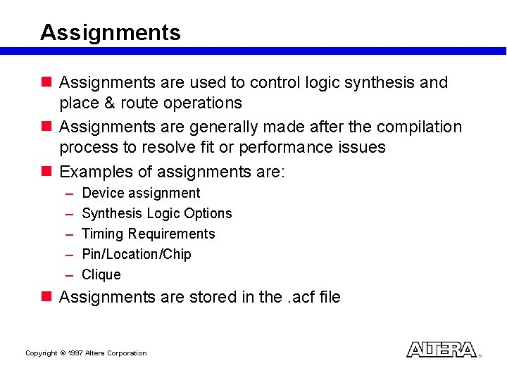
Assignments n Assignments are used to control logic synthesis and place & route operations n Assignments are generally made after the compilation process to resolve fit or performance issues n Examples of assignments are: – – – Device assignment Synthesis Logic Options Timing Requirements Pin/Location/Chip Clique n Assignments are stored in the. acf file Copyright © 1997 Altera Corporation

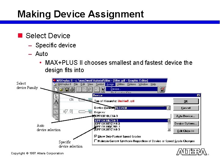
Making Device Assignment n Select Device – Specific device – Auto • MAX+PLUS II chooses smallest and fastest device the design fits into Select device Family Auto device selection Specific device selection Copyright © 1997 Altera Corporation

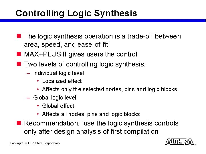
Controlling Logic Synthesis n The logic synthesis operation is a trade-off between area, speed, and ease-of-fit n MAX+PLUS II gives users the control n Two levels of controlling logic synthesis: – Individual logic level • Localized effect • Affects only the selected nodes, pins and logic blocks – Global logic level • Global effect • Affects all nodes, pins and logic blocks n Recommendation: use the logic synthesis controls only after design analysis of first compilation Copyright © 1997 Altera Corporation

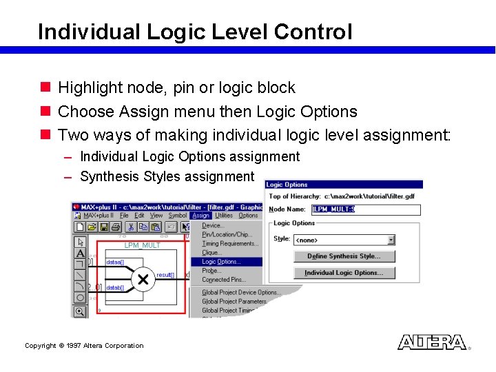
Individual Logic Level Control n Highlight node, pin or logic block n Choose Assign menu then Logic Options n Two ways of making individual logic level assignment: – Individual Logic Options assignment – Synthesis Styles assignment Copyright © 1997 Altera Corporation

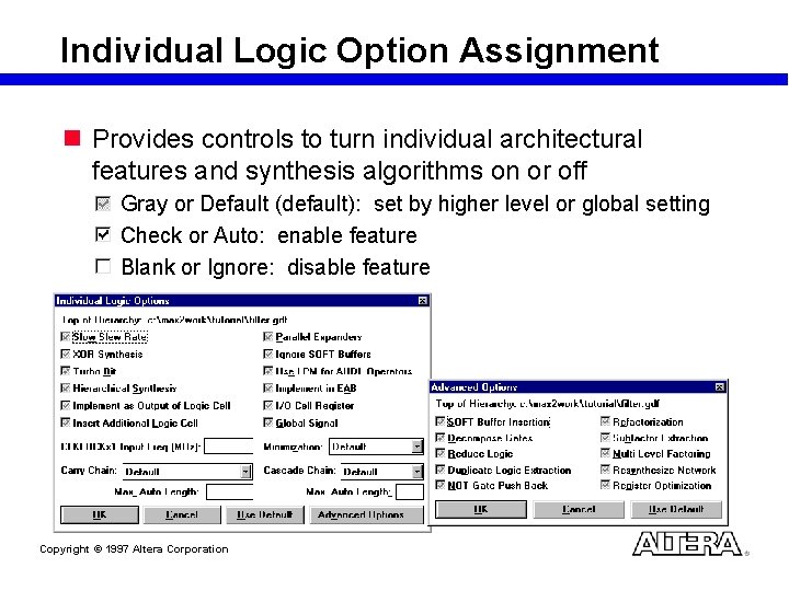
Individual Logic Option Assignment n Provides controls to turn individual architectural features and synthesis algorithms on or off Gray or Default (default): set by higher level or global setting Check or Auto: enable feature Blank or Ignore: disable feature Copyright © 1997 Altera Corporation

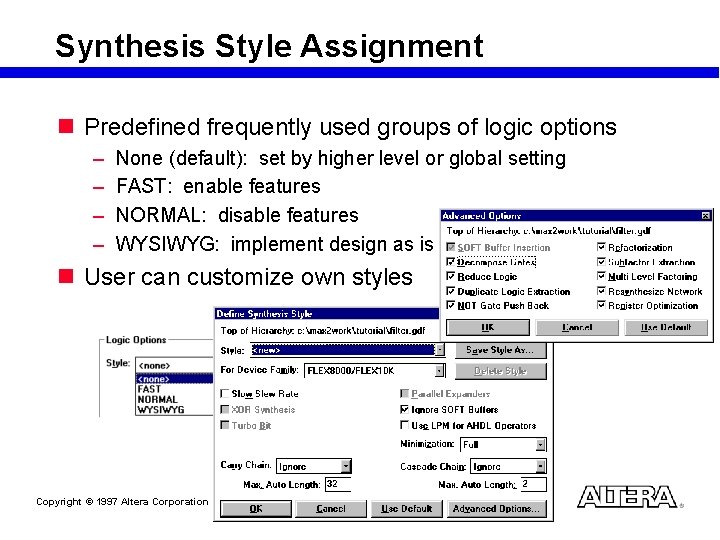
Synthesis Style Assignment n Predefined frequently used groups of logic options – – None (default): set by higher level or global setting FAST: enable features NORMAL: disable features WYSIWYG: implement design as is n User can customize own styles Copyright © 1997 Altera Corporation

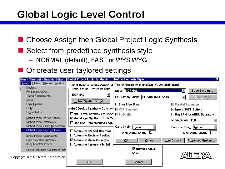
Global Logic Level Control n Choose Assign then Global Project Logic Synthesis n Select from predefined synthesis style – NORMAL (default), FAST or WYSIWYG n Or create user taylored settings Copyright © 1997 Altera Corporation

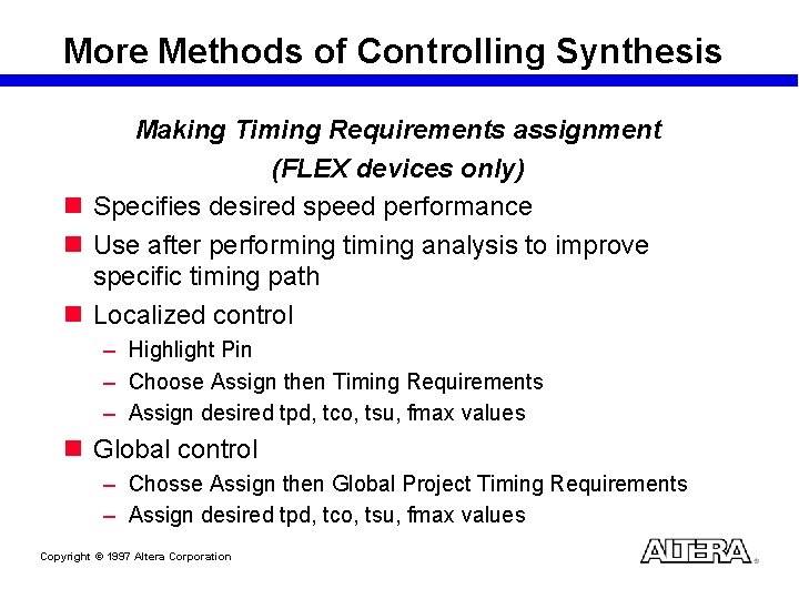
More Methods of Controlling Synthesis Making Timing Requirements assignment (FLEX devices only) n Specifies desired speed performance n Use after performing timing analysis to improve specific timing path n Localized control – Highlight Pin – Choose Assign then Timing Requirements – Assign desired tpd, tco, tsu, fmax values n Global control – Chosse Assign then Global Project Timing Requirements – Assign desired tpd, tco, tsu, fmax values Copyright © 1997 Altera Corporation

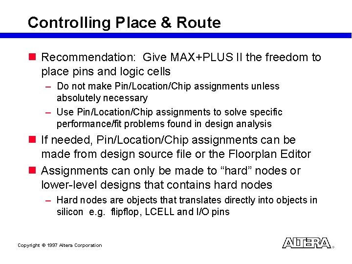
Controlling Place & Route n Recommendation: Give MAX+PLUS II the freedom to place pins and logic cells – Do not make Pin/Location/Chip assignments unless absolutely necessary – Use Pin/Location/Chip assignments to solve specific performance/fit problems found in design analysis n If needed, Pin/Location/Chip assignments can be made from design source file or the Floorplan Editor n Assignments can only be made to “hard” nodes or lower-level designs that contains hard nodes – Hard nodes are objects that translates directly into objects in silicon e. g. flipflop, LCELL and I/O pins Copyright © 1997 Altera Corporation

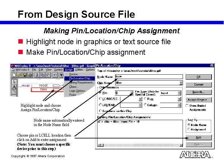
From Design Source File Making Pin/Location/Chip Assignment n Highlight node in graphics or text source file n Make Pin/Location/Chip assignment Highlight node and choose Assign Pin/Location/Chip Node name automatically entered in the Node Name field Choose pin or LCELL location then click on Add to enter assignment (Note: You must choose a specific device prior to this step) Copyright © 1997 Altera Corporation

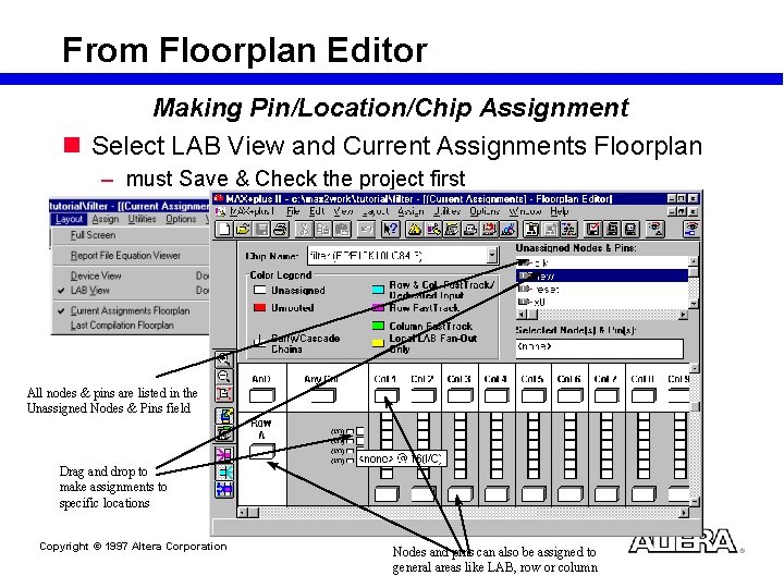
From Floorplan Editor Making Pin/Location/Chip Assignment n Select LAB View and Current Assignments Floorplan – must Save & Check the project first All nodes & pins are listed in the Unassigned Nodes & Pins field Drag and drop to make assignments to specific locations Copyright © 1997 Altera Corporation Nodes and pins can also be assigned to general areas like LAB, row or column

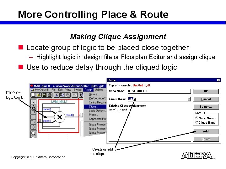
More Controlling Place & Route Making Clique Assignment n Locate group of logic to be placed close together – Highlight logic in design file or Floorplan Editor and assign clique n Use to reduce delay through the cliqued logic Highlight logic block Copyright © 1997 Altera Corporation Create or add to clique

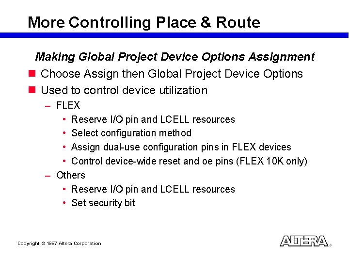
More Controlling Place & Route Making Global Project Device Options Assignment n Choose Assign then Global Project Device Options n Used to control device utilization – FLEX • Reserve I/O pin and LCELL resources • Select configuration method • Assign dual-use configuration pins in FLEX devices • Control device-wide reset and oe pins (FLEX 10 K only) – Others • Reserve I/O pin and LCELL resources • Set security bit Copyright © 1997 Altera Corporation

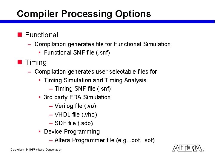
Compiler Processing Options n Functional – Compilation generates file for Functional Simulation • Functional SNF file (. snf) n Timing – Compilation generates user selectable files for • Timing Simulation and Timing Analysis – Timing SNF file (. snf) • 3 rd party EDA Simulation – Verilog file (. vo) – VHDL file (. vho) – SDF file (. sdo) • Device Programming – Altera Programmer file (e. g. . pof, . sof) Copyright © 1997 Altera Corporation

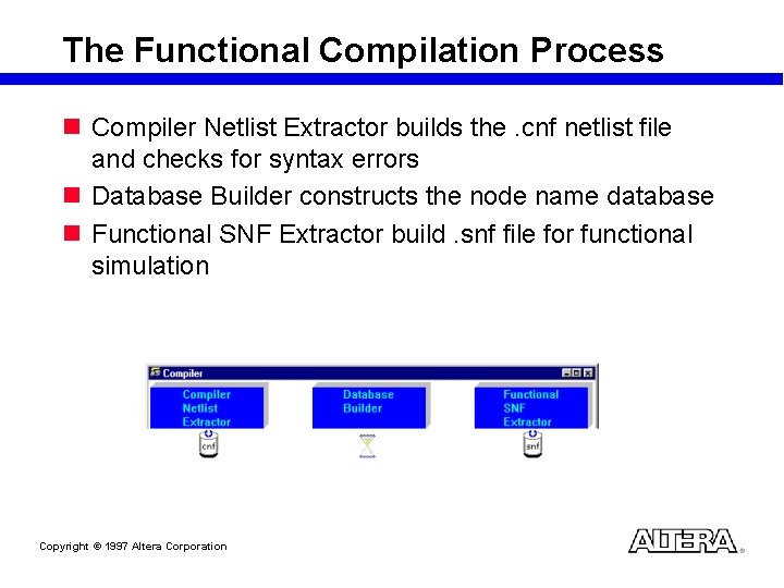
The Functional Compilation Process n Compiler Netlist Extractor builds the. cnf netlist file and checks for syntax errors n Database Builder constructs the node name database n Functional SNF Extractor build. snf file for functional simulation Copyright © 1997 Altera Corporation

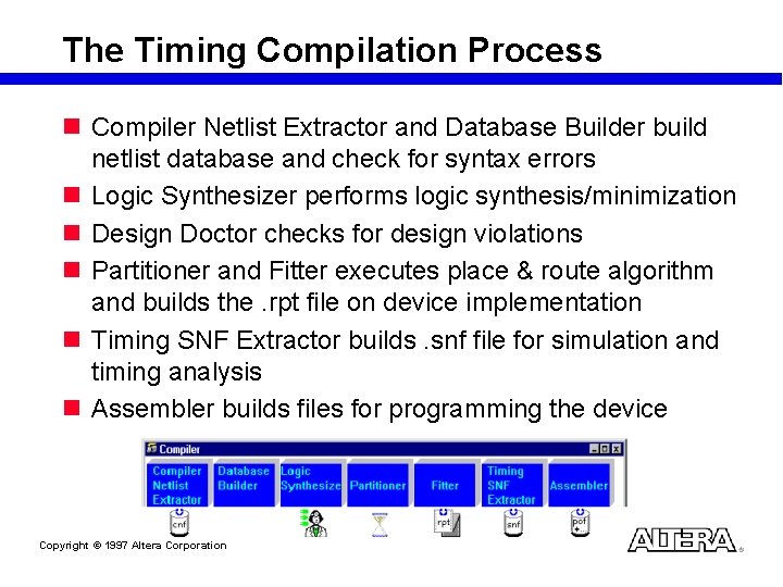
The Timing Compilation Process n Compiler Netlist Extractor and Database Builder build netlist database and check for syntax errors n Logic Synthesizer performs logic synthesis/minimization n Design Doctor checks for design violations n Partitioner and Fitter executes place & route algorithm and builds the. rpt file on device implementation n Timing SNF Extractor builds. snf file for simulation and timing analysis n Assembler builds files for programming the device Copyright © 1997 Altera Corporation

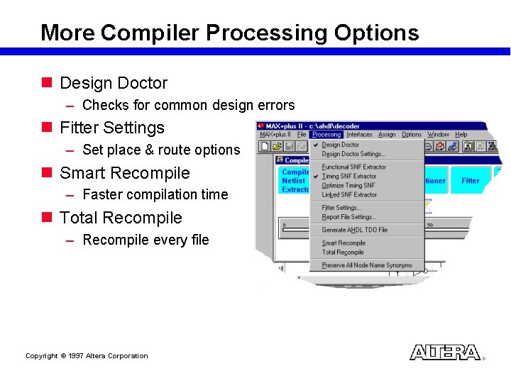
More Compiler Processing Options n Design Doctor – Checks for common design errors n Fitter Settings – Set place & route options n Smart Recompile – Faster compilation time n Total Recompile – Recompile every file Copyright © 1997 Altera Corporation

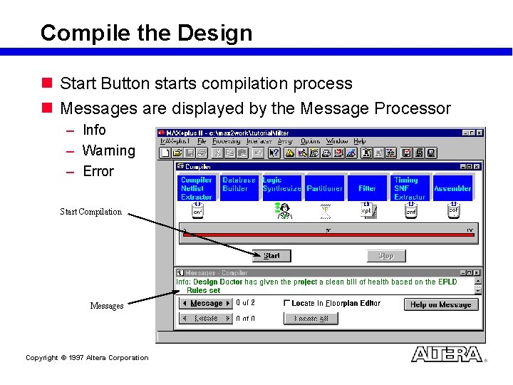
Compile the Design n Start Button starts compilation process n Messages are displayed by the Message Processor – Info – Warning – Error Start Compilation Messages Copyright © 1997 Altera Corporation

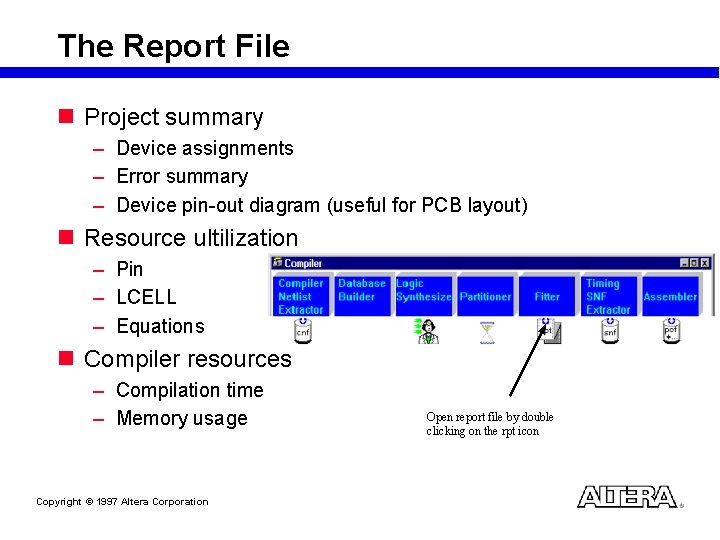
The Report File n Project summary – Device assignments – Error summary – Device pin-out diagram (useful for PCB layout) n Resource ultilization – Pin – LCELL – Equations n Compiler resources – Compilation time – Memory usage Copyright © 1997 Altera Corporation Open report file by double clicking on the rpt icon

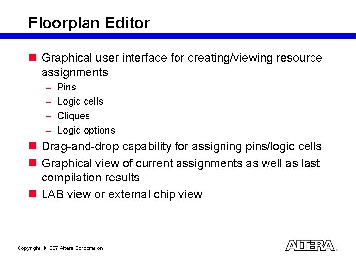
Floorplan Editor n Graphical user interface for creating/viewing resource assignments – – Pins Logic cells Cliques Logic options n Drag-and-drop capability for assigning pins/logic cells n Graphical view of current assignments as well as last compilation results n LAB view or external chip view Copyright © 1997 Altera Corporation

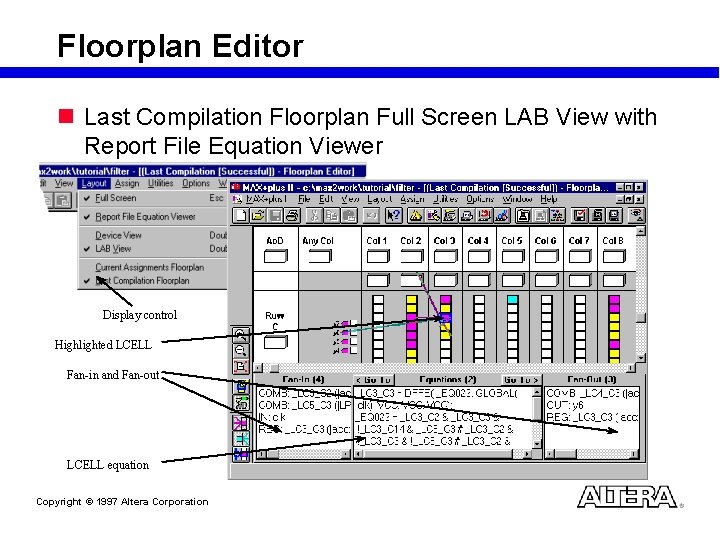
Floorplan Editor n Last Compilation Floorplan Full Screen LAB View with Report File Equation Viewer Display control Highlighted LCELL Fan-in and Fan-out LCELL equation Copyright © 1997 Altera Corporation

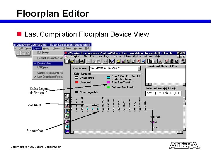
Floorplan Editor n Last Compilation Floorplan Device View Color Legend definition Pin name Pin number Copyright © 1997 Altera Corporation

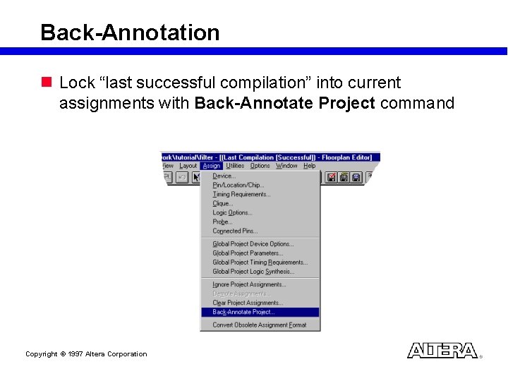
Back-Annotation n Lock “last successful compilation” into current assignments with Back-Annotate Project command Copyright © 1997 Altera Corporation

Example Section (LAB 2) Copyright © 1997 Altera Corporation

Demo 1 (1) Compile the file from previous design (2) Correct the Error (3) Demo the Functional/Timing Compilation step (4) Demo some Assign Option - turn on Cascade/Carry Chain - Synthesis Style Option on different module (5) Step through the RPT file (6) Step through the Floor. Plan Editor Copyright © 1997 Altera Corporation

Project Compilation Recommendations n Use assignments after design analysis to improve fitting or performance n Use the Report File to find specific information on the design n Use the Floorplan Editor to see results of Assignments n Back Annotate your design only when necessary for board layout to give MAX+PLUS II the best chance of fitting design into device Copyright © 1997 Altera Corporation

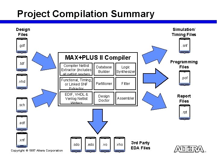
Project Compilation Summary Design Files Simulation/ Timing Files . gdf . snf MAX+PLUS II Compiler. tdf . vhd Compiler Netlist Extractor (includes all netlist readers Database Builder Functional, Timing, or Linked SNF Extractor Partitioner Fitter EDIF, VHDL & Verilog Netlist Writers Design Doctor Assembler . sch Logic Synthesizer Programming Files. pof Report Files. rpt . edf . xnf. sdo Copyright © 1997 Altera Corporation . edo . vho 3 rd Party EDA Files

Design Specification Design Entry Design Modification Project Compilation Simulation Timing Analysis Device Programming In-System Verification System Production Copyright © 1997 Altera Corporation

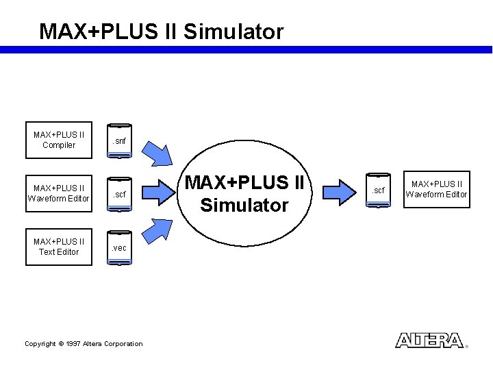
MAX+PLUS II Simulator MAX+PLUS II Compiler . snf MAX+PLUS II Waveform Editor . scf MAX+PLUS II Text Editor . vec Copyright © 1997 Altera Corporation MAX+PLUS II Simulator . scf MAX+PLUS II Waveform Editor

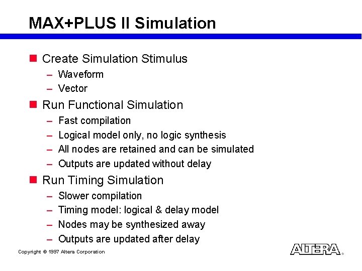
MAX+PLUS II Simulation n Create Simulation Stimulus – Waveform – Vector n Run Functional Simulation – – Fast compilation Logical model only, no logic synthesis All nodes are retained and can be simulated Outputs are updated without delay n Run Timing Simulation – – Slower compilation Timing model: logical & delay model Nodes may be synthesized away Outputs are updated after delay Copyright © 1997 Altera Corporation

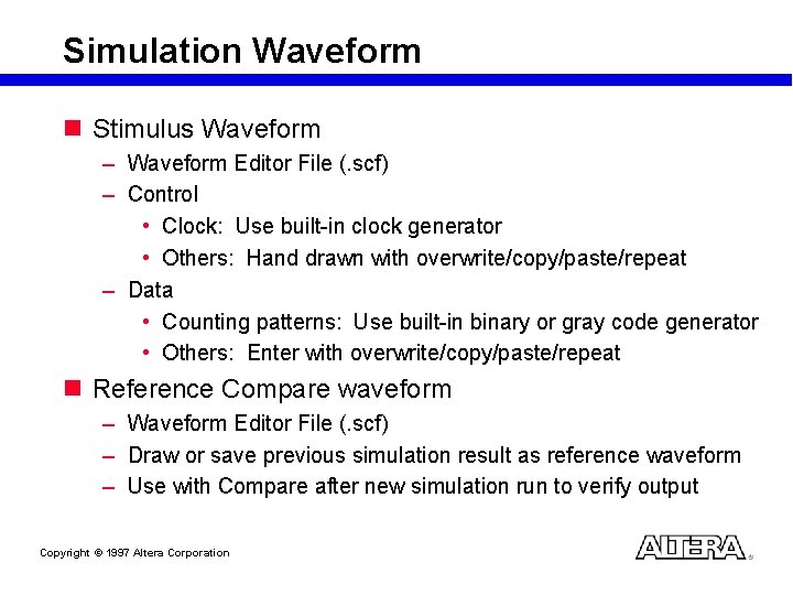
Simulation Waveform n Stimulus Waveform – Waveform Editor File (. scf) – Control • Clock: Use built-in clock generator • Others: Hand drawn with overwrite/copy/paste/repeat – Data • Counting patterns: Use built-in binary or gray code generator • Others: Enter with overwrite/copy/paste/repeat n Reference Compare waveform – Waveform Editor File (. scf) – Draw or save previous simulation result as reference waveform – Use with Compare after new simulation run to verify output Copyright © 1997 Altera Corporation

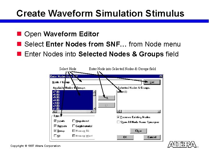
Create Waveform Simulation Stimulus n Open Waveform Editor n Select Enter Nodes from SNF… from Node menu n Enter Nodes into Selected Nodes & Groups field Select Node Copyright © 1997 Altera Corporation Enter Node into Selected Nodes & Groups field

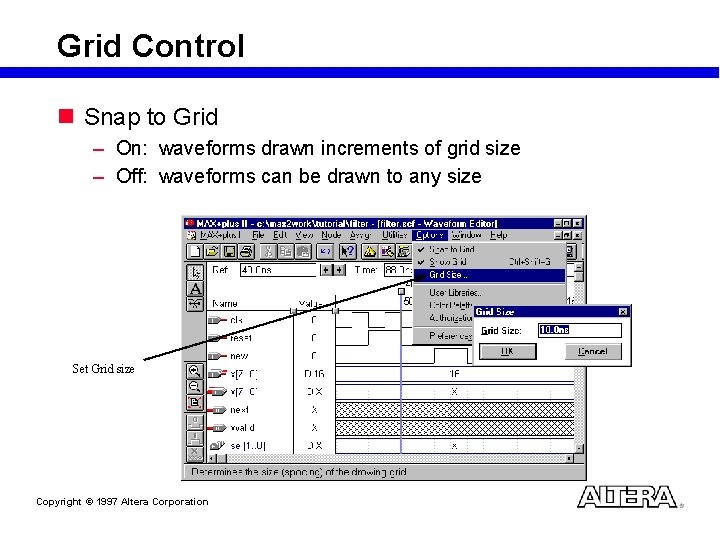
Grid Control n Snap to Grid – On: waveforms drawn increments of grid size – Off: waveforms can be drawn to any size Set Grid size Copyright © 1997 Altera Corporation

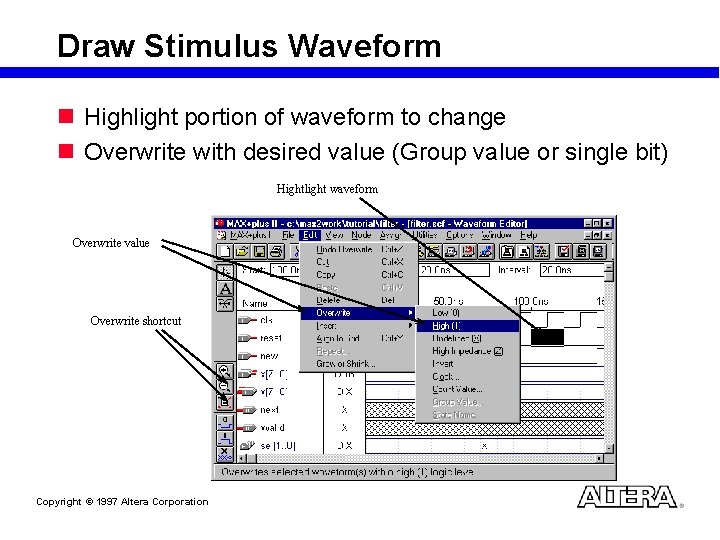
Draw Stimulus Waveform n Highlight portion of waveform to change n Overwrite with desired value (Group value or single bit) Hightlight waveform Overwrite value Overwrite shortcut Copyright © 1997 Altera Corporation

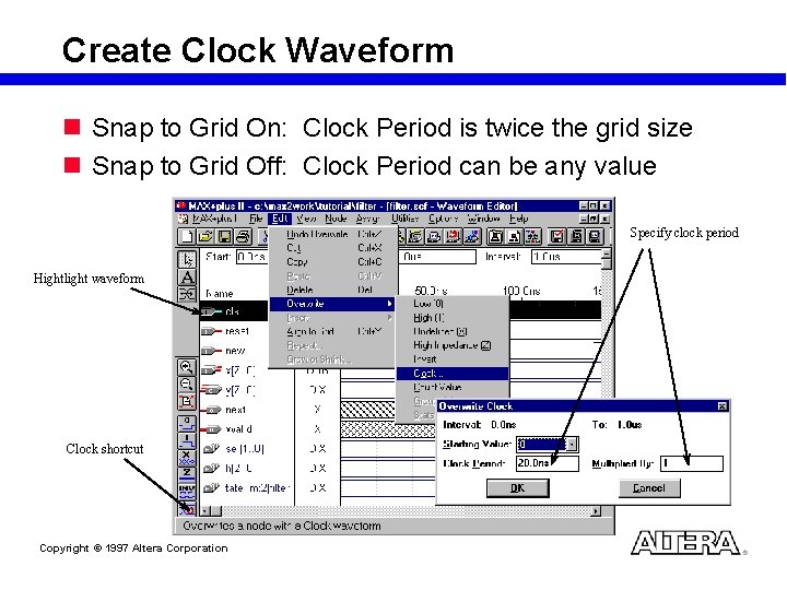
Create Clock Waveform n Snap to Grid On: Clock Period is twice the grid size n Snap to Grid Off: Clock Period can be any value Specify clock period Hightlight waveform Clock shortcut Copyright © 1997 Altera Corporation

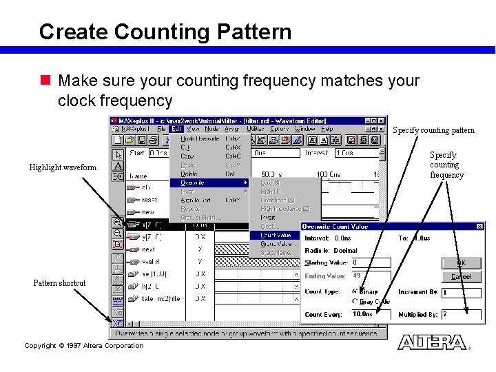
Create Counting Pattern n Make sure your counting frequency matches your clock frequency Specify counting pattern Highlight waveform Pattern shortcut Copyright © 1997 Altera Corporation Specify counting frequency

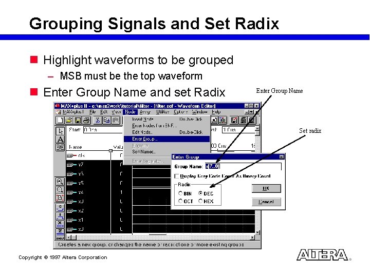
Grouping Signals and Set Radix n Highlight waveforms to be grouped – MSB must be the top waveform n Enter Group Name and set Radix Enter Group Name Set radix Copyright © 1997 Altera Corporation

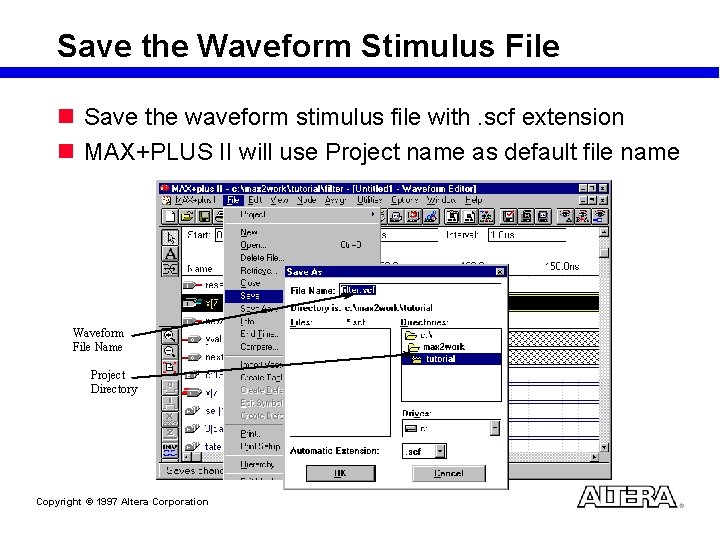
Save the Waveform Stimulus File n Save the waveform stimulus file with. scf extension n MAX+PLUS II will use Project name as default file name Waveform File Name Project Directory Copyright © 1997 Altera Corporation

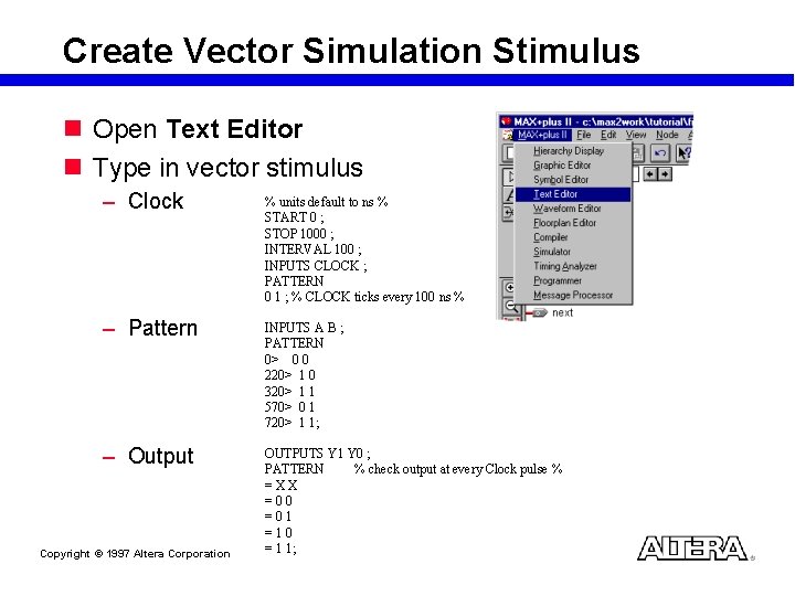
Create Vector Simulation Stimulus n Open Text Editor n Type in vector stimulus – Clock % units default to ns % START 0 ; STOP 1000 ; INTERVAL 100 ; INPUTS CLOCK ; PATTERN 0 1 ; % CLOCK ticks every 100 ns % – Pattern INPUTS A B ; PATTERN 0> 0 0 220> 1 0 320> 1 1 570> 0 1 720> 1 1; – Output OUTPUTS Y 1 Y 0 ; PATTERN % check output at every Clock pulse % =XX =00 =01 =10 = 1 1; Copyright © 1997 Altera Corporation

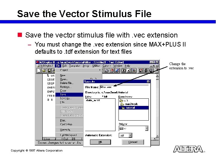
Save the Vector Stimulus File n Save the vector stimulus file with. vec extension – You must change the. vec extension since MAX+PLUS II defaults to. tdf extension for text files Change the extension to. vec Copyright © 1997 Altera Corporation

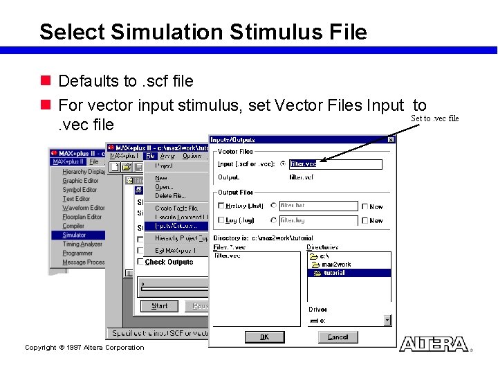
Select Simulation Stimulus File n Defaults to. scf file n For vector input stimulus, set Vector Files Input to Set to. vec file Copyright © 1997 Altera Corporation

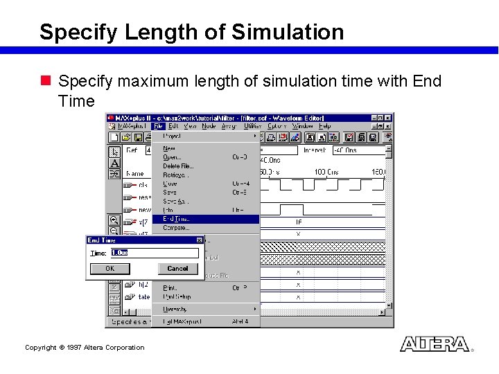
Specify Length of Simulation n Specify maximum length of simulation time with End Time Copyright © 1997 Altera Corporation

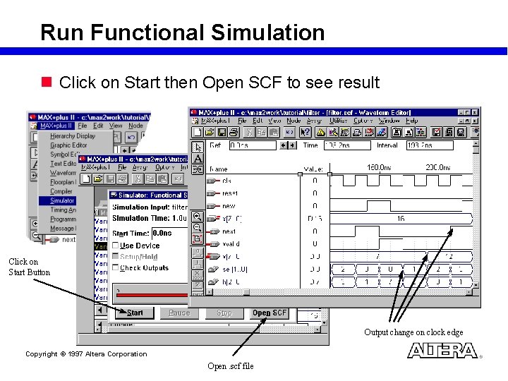
Run Functional Simulation n Click on Start then Open SCF to see result Click on Start Button Output change on clock edge Copyright © 1997 Altera Corporation Open. scf file

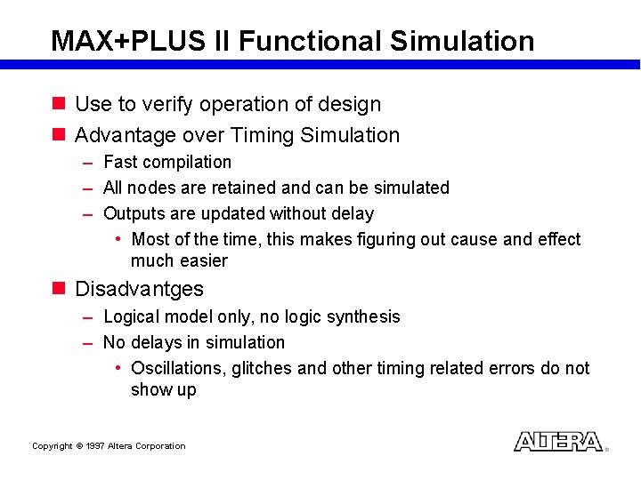
MAX+PLUS II Functional Simulation n Use to verify operation of design n Advantage over Timing Simulation – Fast compilation – All nodes are retained and can be simulated – Outputs are updated without delay • Most of the time, this makes figuring out cause and effect much easier n Disadvantges – Logical model only, no logic synthesis – No delays in simulation • Oscillations, glitches and other timing related errors do not show up Copyright © 1997 Altera Corporation

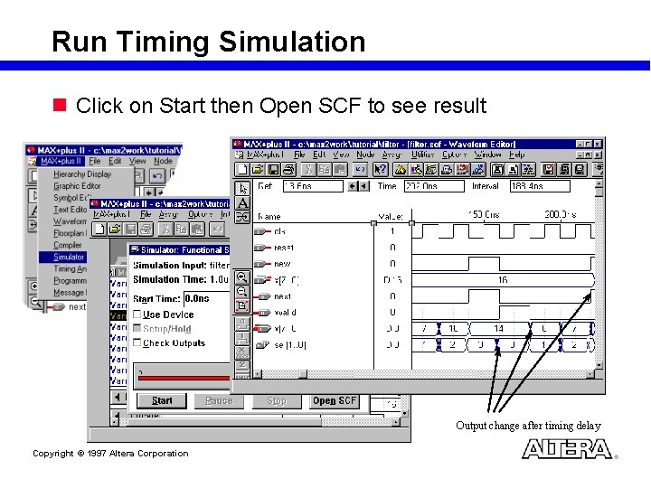
Run Timing Simulation n Click on Start then Open SCF to see result Output change after timing delay Copyright © 1997 Altera Corporation

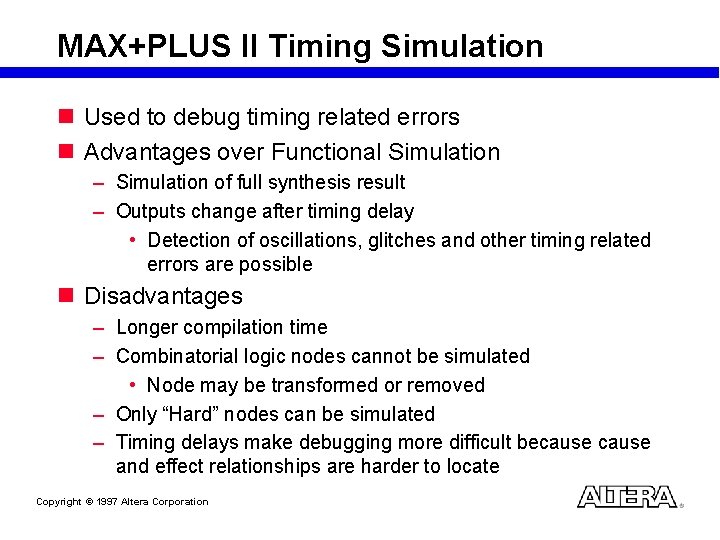
MAX+PLUS II Timing Simulation n Used to debug timing related errors n Advantages over Functional Simulation – Simulation of full synthesis result – Outputs change after timing delay • Detection of oscillations, glitches and other timing related errors are possible n Disadvantages – Longer compilation time – Combinatorial logic nodes cannot be simulated • Node may be transformed or removed – Only “Hard” nodes can be simulated – Timing delays make debugging more difficult because and effect relationships are harder to locate Copyright © 1997 Altera Corporation

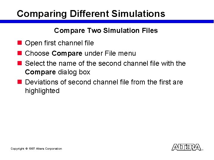
Comparing Different Simulations Compare Two Simulation Files n Open first channel file n Choose Compare under File menu n Select the name of the second channel file with the Compare dialog box n Deviations of second channel file from the first are highlighted Copyright © 1997 Altera Corporation

Example Section (LAB 3) Copyright © 1997 Altera Corporation

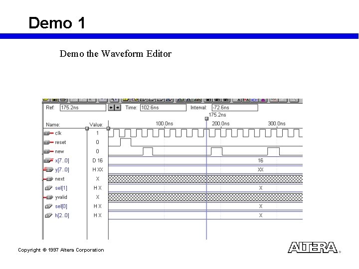
Demo 1 Demo the Waveform Editor Copyright © 1997 Altera Corporation

Project Simulation Recommendations n n n Use built-in clock generator to create clock Use built-in count generator to create test pattern Use Functional Simulation to verify properation Use Timing Simulation to examine signal delay effects Use Compare function to verify output Use the dynamic link ( Find Node in Design File ) to go to source file to make any necessary corrections Copyright © 1997 Altera Corporation

Project Simulation Summary n Two types of simulation – Functional simulation • No logic synthesis • No delay model • All nodes can be simulated – Timing simulation • Logic synthesis • Delay model • Only hard nodes can be simulated n Two types of stimulus file – Waveform – Vector n Simulation result is stored in. scf file Copyright © 1997 Altera Corporation

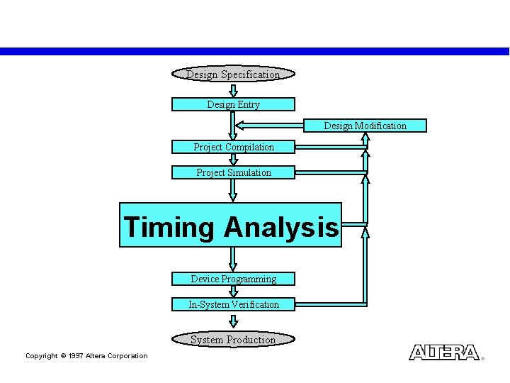
Design Specification Design Entry Design Modification Project Compilation Project Simulation Timing Analysis Device Programming In-System Verification System Production Copyright © 1997 Altera Corporation

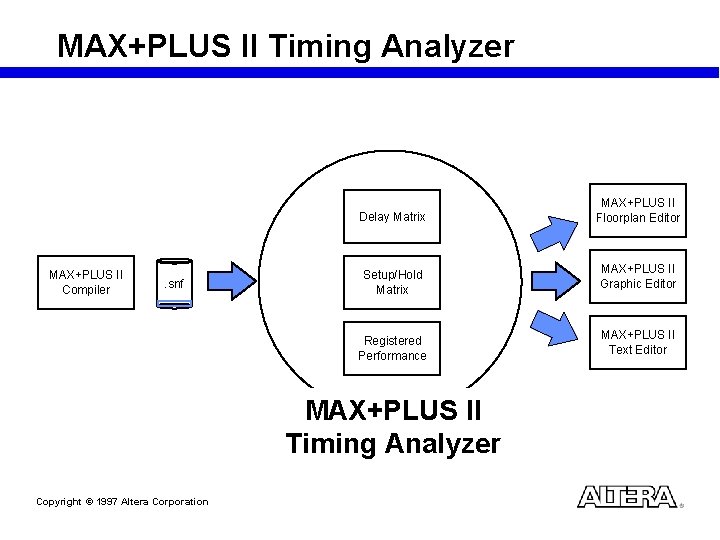
MAX+PLUS II Timing Analyzer Delay Matrix MAX+PLUS II Compiler . snf Setup/Hold Matrix Registered Performance MAX+PLUS II Timing Analyzer Copyright © 1997 Altera Corporation MAX+PLUS II Floorplan Editor MAX+PLUS II Graphic Editor MAX+PLUS II Text Editor

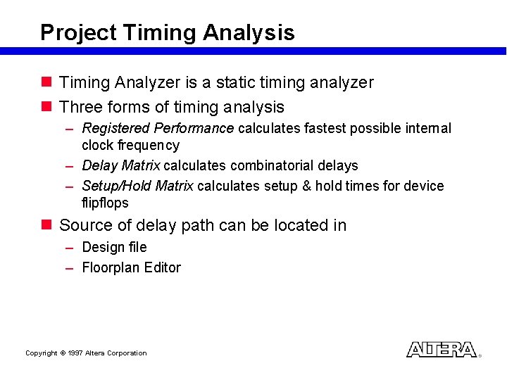
Project Timing Analysis n Timing Analyzer is a static timing analyzer n Three forms of timing analysis – Registered Performance calculates fastest possible internal clock frequency – Delay Matrix calculates combinatorial delays – Setup/Hold Matrix calculates setup & hold times for device flipflops n Source of delay path can be located in – Design file – Floorplan Editor Copyright © 1997 Altera Corporation

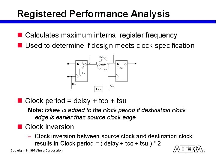
Registered Performance Analysis n Calculates maximum internal register frequency n Used to determine if design meets clock specification n Clock period = delay + tco + tsu Note: tskew is added to the clock period if destination clock edge is earlier than source clock edge n Clock inversion – Clock inversion between source clock and destination clock results in Clock period = ( delay + tco + tsu ) * 2 Copyright © 1997 Altera Corporation

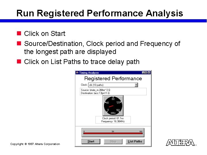
Run Registered Performance Analysis n Click on Start n Source/Destination, Clock period and Frequency of the longest path are displayed n Click on List Paths to trace delay path Copyright © 1997 Altera Corporation

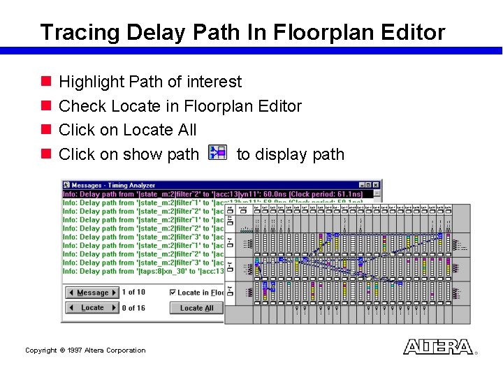
Tracing Delay Path In Floorplan Editor n n Highlight Path of interest Check Locate in Floorplan Editor Click on Locate All Click on show path to display path Copyright © 1997 Altera Corporation

Application of Registered Performance n Use Registered Performance Analysis to see if design meets clock frequency requirement n What to do if frequency is less than desired – Use List Path to display the worst case delays – Use Floorplan Editor to view the entire path • Are Logic Cells and pins scattered among different rows? • Can the Logic Cells benefit from carry/cascade chains (FLEX) or parallel expanders (MAX)? – Use Assignments ( Clique, Logic Options, etc… ) on the critical path to improve performance – If still less than desired, consider pipelining technique or different design implementations where appropriate Copyright © 1997 Altera Corporation

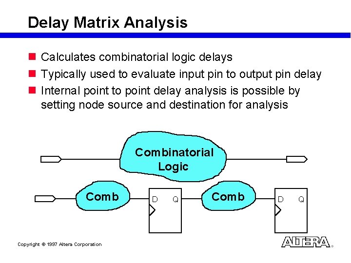
Delay Matrix Analysis n Calculates combinatorial logic delays n Typically used to evaluate input pin to output pin delay n Internal point to point delay analysis is possible by setting node source and destination for analysis Combinatorial Logic Comb Copyright © 1997 Altera Corporation D Q Comb D Q

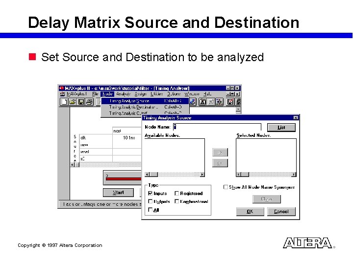
Delay Matrix Source and Destination n Set Source and Destination to be analyzed Copyright © 1997 Altera Corporation

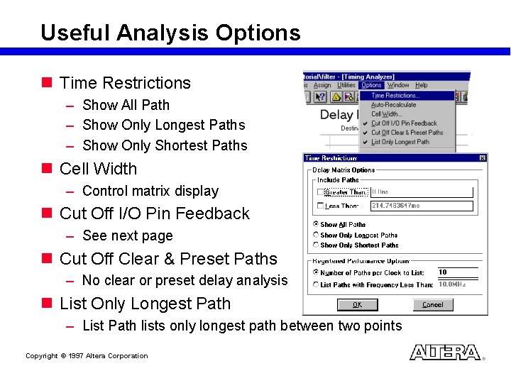
Useful Analysis Options n Time Restrictions – Show All Path – Show Only Longest Paths – Show Only Shortest Paths n Cell Width – Control matrix display n Cut Off I/O Pin Feedback – See next page n Cut Off Clear & Preset Paths – No clear or preset delay analysis n List Only Longest Path – List Path lists only longest path between two points Copyright © 1997 Altera Corporation

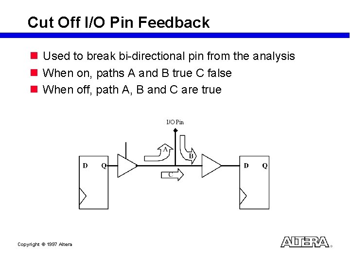
Cut Off I/O Pin Feedback n Used to break bi-directional pin from the analysis n When on, paths A and B true C false n When off, path A, B and C are true I/O Pin Copyright © 1997 Altera Corporation

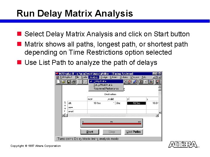
Run Delay Matrix Analysis n Select Delay Matrix Analysis and click on Start button n Matrix shows all paths, longest path, or shortest path depending on Time Restrictions option selected n Use List Path to analyze the path of delays Copyright © 1997 Altera Corporation

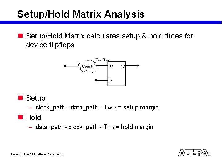
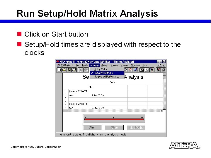
Setup/Hold Matrix Analysis n Setup/Hold Matrix calculates setup & hold times for device flipflops n Setup – clock_path - data_path - Tsetup = setup margin n Hold – data_path - clock_path - Thold = hold margin Copyright © 1997 Altera Corporation

Run Setup/Hold Matrix Analysis n Click on Start button n Setup/Hold times are displayed with respect to the clocks Copyright © 1997 Altera Corporation

Example Section (LAB 4) Copyright © 1997 Altera Corporation

Demo 1 (1) Compile the previous design by Timing Compilation (2) Run the Timing Analysis - Delay Matrix - Setup/Hold time Matrix - Clock Performance (3) Play around with some Timing Analysis Option Copyright © 1997 Altera Corporation

Timing Analysis Recommendations n Use Timing Analyzer to locate performance bottleneck n Use Registered Performance Analysis to determine internal clock frequency performance of the design n Use Show Only Longest Path Time Restrictions in Delay Matrix to get the longest delay time from input pin to output pin n Use List Path and Locate in Floorplan Editor to view worst case paths n Use List Path and Locate to trace through path in design file n Use assignments and recompile to fine-tune performance Copyright © 1997 Altera Corporation

Project Timing Analysis Summary n Timing Analyzer is a static timing analyzer n Three modes of Timing Analysis – Registered Performance – Delay Matrix – Setup/Hold Matrix n Provides ability to trace path through Floorplan Editor or design file Copyright © 1997 Altera Corporation

Design Specification Design Entry Design Modification Project Compilation Project Simulation Timing Analysis Device Programming In-System Verification Copyright © 1997 Altera Corporation System Production

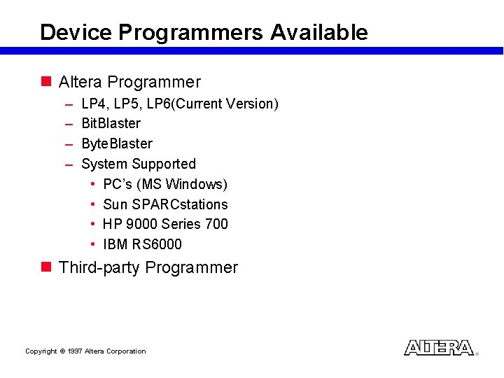
Device Programmers Available n Altera Programmer – – LP 4, LP 5, LP 6(Current Version) Bit. Blaster Byte. Blaster System Supported • PC’s (MS Windows) • Sun SPARCstations • HP 9000 Series 700 • IBM RS 6000 n Third-party Programmer Copyright © 1997 Altera Corporation

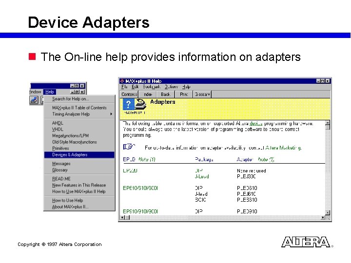
Device Adapters n The On-line help provides information on adapters Copyright © 1997 Altera Corporation

Programming a Device Using the Programmer & the MPU n Initiate programming with the Programmer module in MAX+PLUS II n Programmer defaults to programming file for specified project n Use Select Programming File (File menu) to select another programming file n Perform programming operation with buttons in Programmer n Master Programming Unit (MPU) stores last command (use Start button to repeat) Copyright © 1997 Altera Corporation

Altera Design Methodology The Big Picture Copyright © 1997 Altera Corporation

Hierarchical Design n Break design into modules n Enter and debug each module separately n Create Default Symbols or Include Files for each module n Use these modules in the top-level design file n Assign each module with individual logic options, if necessary Copyright © 1997 Altera Corporation

Compile n Select the targeted device n Remember the 80/80 rule. Reserve 20% logic and 20% I/O pin resources to accommodate potential design modifications n Compile top-level design without any pin assignments first to determine if the design actually fits in the targeted device n If absolutely necessary, pin and logic locations can be assigned through design editor or Floorplan Editor or directly to the assignment & configuration file (. acf) Copyright © 1997 Altera Corporation

Verify n Simulate. – Functionally correct? – Any glitches? n Perform Timing Analysis – Resolve performance bottlenecks n Satisfied with design: Back annotate Project to lock down pin and logic option assignments Copyright © 1997 Altera Corporation

Program n Program the device n Run system verification tests n If necessary, modify the design, recompile with the back annotated assignments and reprogram the device Copyright © 1997 Altera Corporation