Designing Smart HallEffect Sensors over Conventional IC processes


 • Hall Effect : For any given material with 4 square-corner")
 • Smart Sensor : signal conditioning is integrated in a chip")
 • Applications want to sense with high")
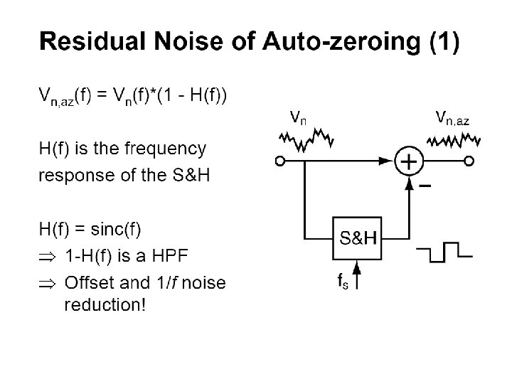
 • • How much offset does the")

 + • • -")
 - At room temp")


")

 Unit 2")
 1 MHz 400")
 1/f reduction INPUT CHOPPER FLICKER")


- Slides: 31
Designing Smart Hall-Effect Sensors over Conventional IC processes. Part 1 Gerardo Monreal – Hernan Romero Allegro Microsystems Argentina 21/07/06 @ UNS – Bahia Blanca.
Allegro World. Wide Facts – – Allegro is successor to Sprague Semi Group, over 2, 500 employees worldwide, headquartered in Worcester, MA, The Company also has manufacturing as well as sales, design and marketing offices in Scotland, UK, France and Argentina. – Sales are balanced worldwide – The Company is ISO 9000 and QS-9000 registered. – Allegro is owned by Sanken Electric Co. (Japan)
Allegro Argentina Facts. • Established in 2001 – However since 1981 Mr. Alberto Bilotti worked as consultant. • • • 6 Design Eng, 5 Layout Eng, 2 Product Eng. Develops Products for the Sensor BU Portfolio. Emphasis in High-End front-end Solutions. More than 15 complete products fully designed in ARG. Complete IC design LAB: – Full Simulation tools. (Cadence: Sch + Layout). – Full Characterization analysis • Auto wafer level test, -40 C to 150 C. • Auto Packaged level analysis.
Some Definitions… (1) • Hall Effect : For any given material with 4 square-corner contacts, if a current (I) is forced in a diagonal THEN a voltage is generated which is proportional to the material mobility. I F = q. E + qv x B B
Some Definitions… (2) • Smart Sensor : signal conditioning is integrated in a chip in such a way that non-idealities (offset, noise, sensitivity) are reduced as much as possible. • Over Regular IC processes: means that the sensor cell itself can be manufactured using regular layers present on the process flow.
What do we design for ? (1) • Applications want to sense with high Accuracy. – Position Intensity of B – Speed & Direction Intensity B – Current Intensity of B However the Hall Cell Sensor is not ideal OFFSET (at B=0, output is not 0 V). NOISE (at B=0, ouput is not purely “DC”) SENSITIVITY (spread, temp, non linearity, etc. . )
What do we design for ? (2) • • How much offset does the CELL have ? How much offset does the Input Amplifier have ? How much NOISE do the CELL and the AMP have ? Are those large compared to what we want to sense ? – SENS is approx 15 uv/G (WEAK we are in trouble). • Solutions: – Static Techniques for CELLS (Quads). – Dynamic Techniques for CELLS + AMPLIFIERS • Trimming • Auto zeroing • Chopping – Techniques for NOISE REDUCTION • Device level optimization (sizing and biasing) • Chopping again
Hall Sensor System overview Switch/Latch Linear Hall sensor FRONT END Input switches Input amp Signal recovery BACK END LPF Output amp Comparator OUTPUT INTERFACE Most of the offset, noise and sensitivity problems are here!!!
How we reduce HALL CELL offset ? Static Techniques (QUADS) + • • - + + - Dynamic Techniques (current spinnig) + CELL Offset is spatially averaged, thus highly reduced Residual offset depends on individual offset contribution mismatches + Phase 0 Phase 90 Current QUADS spinning Offset from each single cell can be Celloffsetreducedtotoalmost +/- 100 uv zero as high as 10 mv!!!
How we reduce HALL CELL noise ? Current driving (CD) - At room temp SNR is worse than VD - At 150 C is the same as VD - Sensitivity linearity over temp is better Voltage driving (VD) -At room temp SNR is better than CD -At 150 C is the same as CD -Sensitivity over temp is parabolic
How we reduce INPUT AMPLIFIER offset ?
AUTOZEROING
Offset Trimming
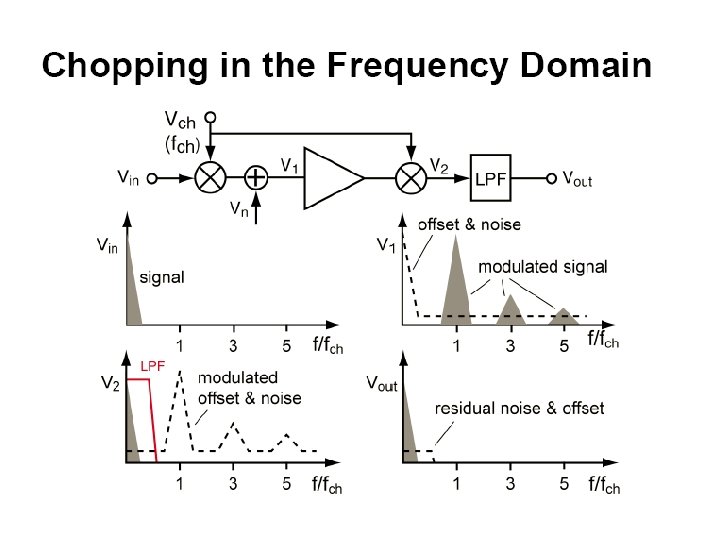
CHOPPING (the way to go)
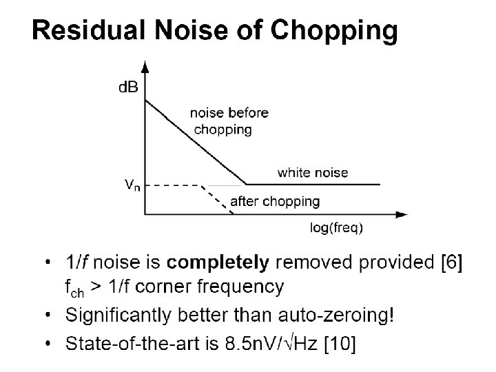
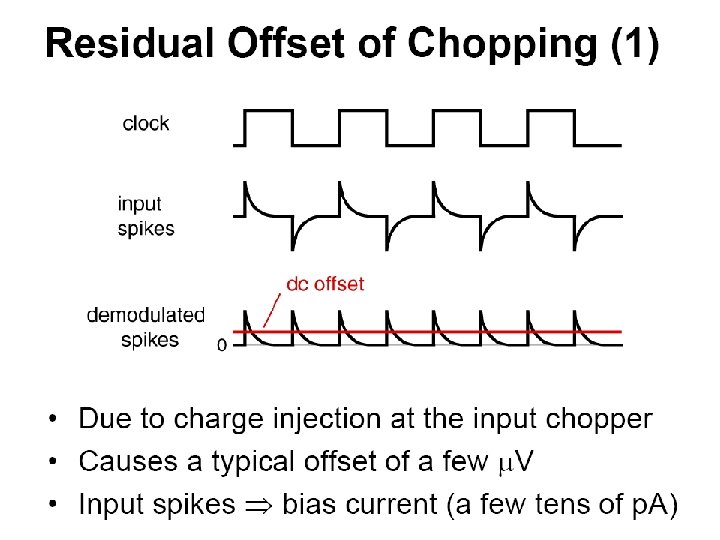
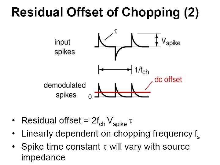
Residual offset of chopping…. how we reduce it?
Some results from the actual world - offset CHOPPER-STABILIZED AMP Residual OFF=F(fck) Unit 2 Unit 3 Unit 4 Unit 5 700 DC OFFSET 600 VSH IS ON 400 300 200 100 200 400 freq [KHz] 600 800 1000 Output referred (G=115 x) 500 Res off ][mv] Unit 1
Some results from the actual world – ripple Ripple (modulated offset) 1 MHz 400 KHz 800 KHz 200 KHz 600 KHz 100 KHz
Some results from the actual world – noise (1) 1/f reduction INPUT CHOPPER FLICKER NOISE POST-CH LPF f f. CK f fk ~ 2 KHz ~ 90 nv/ Hz
However… • • How do we ADD amplifier + Hall Cell offsets ? What freq do we chop at ? What about noise modulation ? What about the LPF recovery system ? – Is it too large ? Too much delay ? • For many years Patented technique SH RECOVERY was used. • NO LPF (but Sinc Filter) , No delay. but Aliasing Noise. • Just now new ideas are being developed to use Topologies that combine no LPF with low noise amplifiers (aliasing free).
Chopper with SH RECOVERY First DOC FE improvement: SH RECOVERY chopper (1995 – DB 2) Goal was to obtain a relaxed LPF, with small area and delay LPF A Vsig Voff Demodulation + S&H Vsig Voff
Chopper Amplifiers
Conclusions - Hall cell : Current spinning allows to separate Hall cell offset from signal offset or signal could be modulated (chopped) - Input Amplifier: - Chopping is the most suited DOC technique for high accuracy (low offset, low noise) systems + Totally removes 1/f noise and offset - Limits amplifier bandwidth - SH RECOVERY + Helps reduce delay with small area - Introduces aliasing - Hall Cell and Amplifier offset can be added in the base band while the signal is modulated.
We have the signal … now what ? • Offset was reduced, Gain stabilized over temp… what else ? • Process Variations & Application errors Trimming. – Needs to be NON-VOLATILE memory. Poly fuses. • Bank of fuses to affect analog parameters (Gain, Sens, etc) • Can also be EEprom … but 150 C is a problem. • Output the signal What format ? – Binary (H or L)… if B>Bop , Vout = L or B<Brp , Vout = H // Bop-Brp=Bhy – Linear … requires output amplifier (class A or AB), Ro < 10 ohm. – Digitized , need a AD converter. High resolution (12 bit)… sigma-delta.