Designing Embedded Systems with PIC Microcontrollers Principles and
Designing Embedded Systems with PIC Microcontrollers: Principles and Applications 2 nd Edition. Tim Wilmshurst Chapter 3 Parallel Ports, Power Supply and the Clock Oscillator The aims of this chapter are to introduce: • Why we need parallel input/output; • • • How simple parallel i/o logic circuits can be developed; How external devices can be connected to the parallel port; The parallel i/o available on the PIC 16 F 84 A; The essential features of power supply and clock oscillator; The Microchip approach to power supply and oscillator; The hardware design of the electronic ping-pong game. Instructors using Designing Embedded Systems with PIC Microcontrollers are welcome to use or change these slides as they see fit. Feedback, to t. j. wilmshurst@derby. ac. uk, is welcomed. The copyright to all diagrams is held by Microchip Technology, or T. Wilmshurst, unless otherwise stated
Why Digital Input/Output? Almost any embedded system needs to transfer digital data between its CPU and the outside world. This transfer falls into a number of categories, which can be summarised as: Direct user interface, including switches, keypads, light emitting diodes (leds) and displays; Input measurement information, from external sensors, possibly being acquired through an analog to digital converter; Output control information, for example to motors or other actuators; Bulk data transfer to or from other systems or sub-systems, moving in serial or parallel form, for example sending serial data to an external memory. How can we provide the required interface between the microcontroller core and the outside world? More precisely, how do we get the data onto or off the data bus at the right moment?
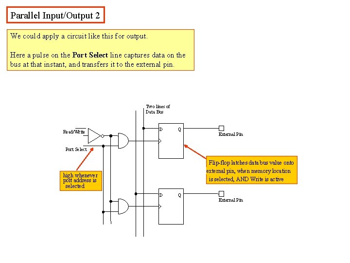
Parallel Input/Output 2 We could apply a circuit like this for output. Here a pulse on the Port Select line captures data on the bus at that instant, and transfers it to the external pin. Two lines of Data Bus Read/Write D Q External Pin Port Select Flip-flop latches data bus value onto external pin, when memory location is selected, AND Write is active high whenever port address is selected D Q External Pin
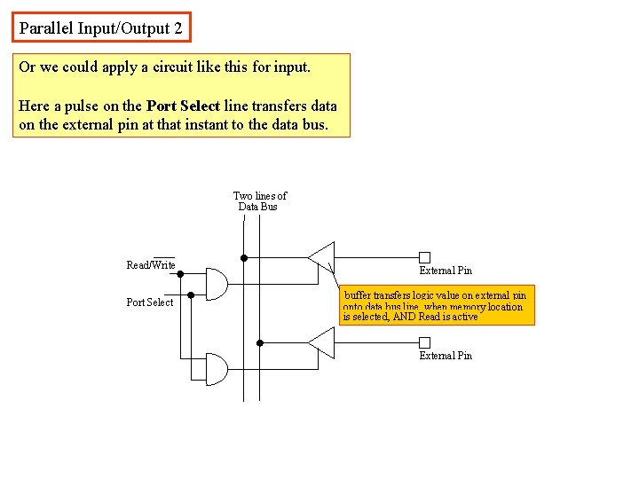
Parallel Input/Output 2 Or we could apply a circuit like this for input. Here a pulse on the Port Select line transfers data on the external pin at that instant to the data bus. Two lines of Data Bus Read/Write Port Select External Pin buffer transfers logic value on external pin onto data bus line, when memory location is selected, AND Read is active External Pin
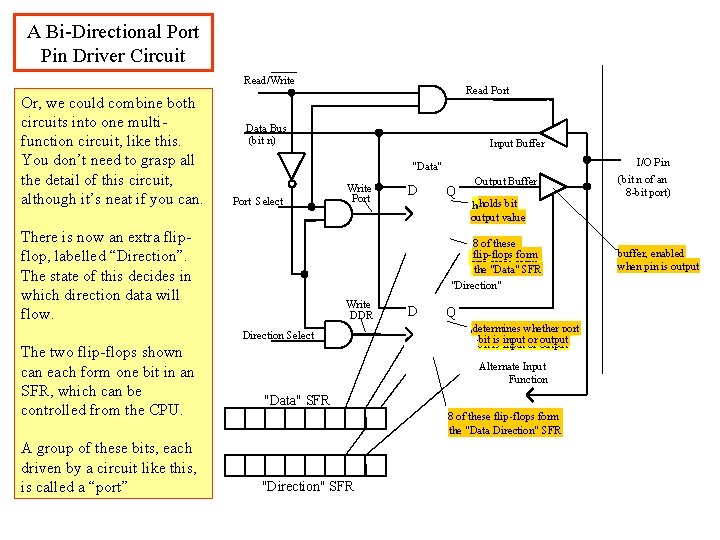
A Bi-Directional Port Pin Driver Circuit Read/Write Or, we could combine both circuits into one multifunction circuit, like this. You don’t need to grasp all the detail of this circuit, although it’s neat if you can. Read Port Data Bus (bit n) Input Buffer Port Select There is now an extra flipflop, labelled “Direction”. The state of this decides in which direction data will flow. Write Port A group of these bits, each driven by a circuit like this, is called a “port” D Q Output Buffer holdsbitbit holds output value 88 of of these flip-flops form the "Data" SFR "Direction" Write DDR Direction Select The two flip-flops shown can each form one bit in an SFR, which can be controlled from the CPU. I/O Pin "Data" D Q determines whether port determines bit is input or output Alternate Input Function "Data" SFR 8 of these flip-flops form the "Data Direction" SFR "Direction" SFR (bit n of an 8 -bit port) buffer, enabled when pin is output
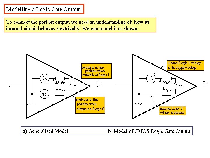
Modelling a Logic Gate Output To connect the port bit output, we need an understanding of how its internal circuit behaves electrically. We can model it as shown. VLH VLL switch is in this position when output is at Logic 1 R S(high) VL R S(low) VS R S(high) R S(low) switch is in this position when output is at Logic 0 a) Generalised Model internal Logic 1 voltage is the supply voltage internal Logic 0 voltage is ground b) Model of CMOS Logic Gate Output VL
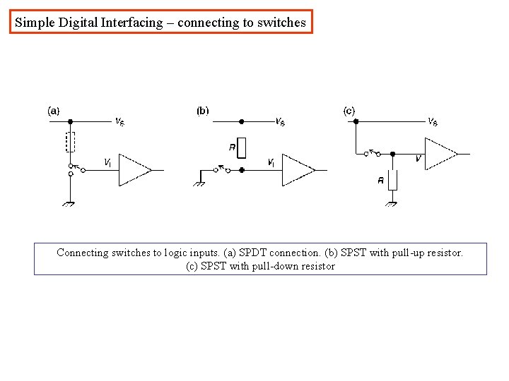
Simple Digital Interfacing – connecting to switches Connecting switches to logic inputs. (a) SPDT connection. (b) SPST with pull-up resistor. (c) SPST with pull-down resistor
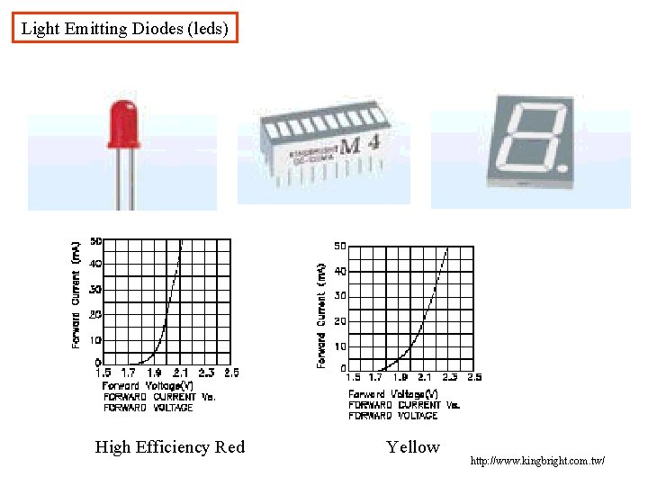
Light Emitting Diodes (leds) High Efficiency Red Yellow http: //www. kingbright. com. tw/
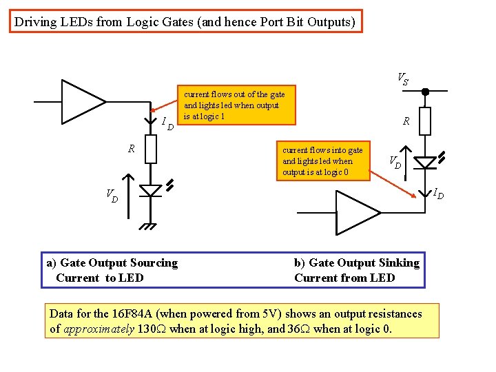
Driving LEDs from Logic Gates (and hence Port Bit Outputs) VS ID R current flows out of the gate and lights led when output is at logic 1 R current flows into gate and lights led when output is at logic 0 VD ID VD a) Gate Output Sourcing Current to LED b) Gate Output Sinking Current from LED Data for the 16 F 84 A (when powered from 5 V) shows an output resistances of approximately 130 when at logic high, and 36 when at logic 0.
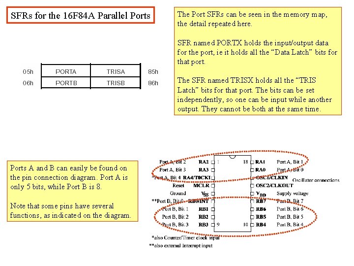
SFRs for the 16 F 84 A Parallel Ports The Port SFRs can be seen in the memory map, the detail repeated here. SFR named PORTX holds the input/output data for the port, ie it holds all the “Data Latch” bits for that port. The SFR named TRISX holds all the “TRIS Latch” bits for that port. The bits can be set independently, so one can be input while another output. They cannot be both at the same time. Ports A and B can easily be found on the pin connection diagram. Port A is only 5 bits, while Port B is 8. Note that some pins have several functions, as indicated on the diagram.
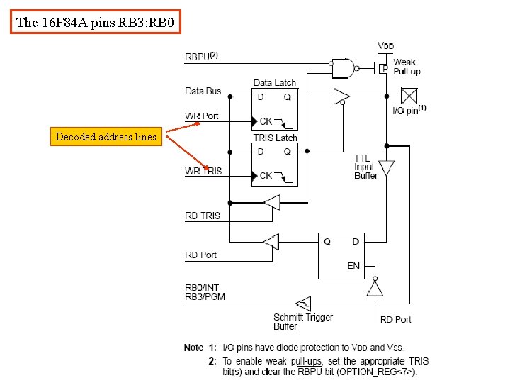
The 16 F 84 A pins RB 3: RB 0 Decoded address lines
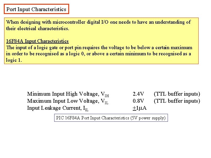
Port Input Characteristics When designing with microcontroller digital I/O one needs to have an understanding of their electrical characteristics. 16 F 84 A Input Characteristics The input of a logic gate or port pin requires the voltage to be below a certain maximum in order to be recognised as a logic 0, or above a certain minimum to be recognised as a logic 1. Minimum Input High Voltage, VIH Maximum Input Low Voltage, VIL Input Leakage Current, IIL 2. 4 V 0. 8 V +1 A (TTL buffer inputs) PIC 16 F 84 A Port Input Characteristics (5 V power supply)
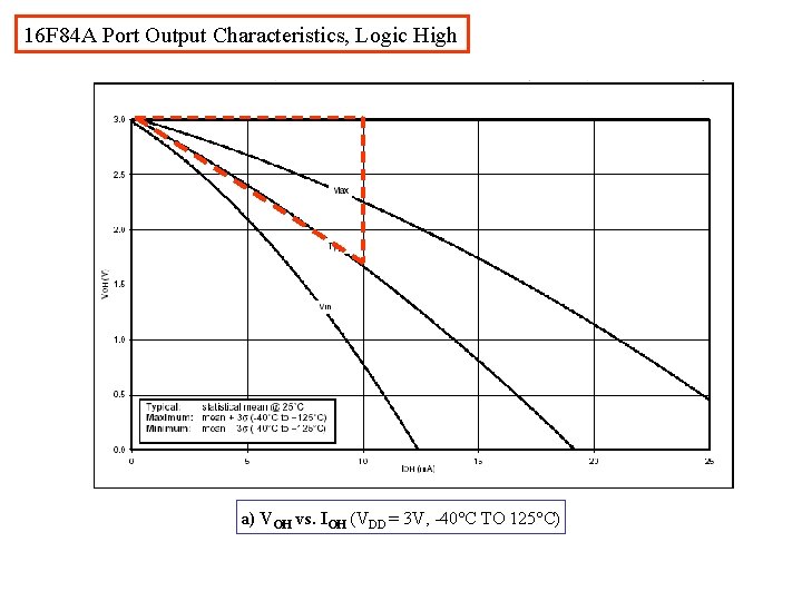
16 F 84 A Port Output Characteristics, Logic High a) VOH vs. IOH (VDD = 3 V, -40°C TO 125°C)
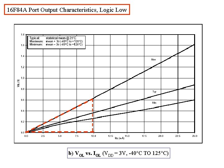
16 F 84 A Port Output Characteristics, Logic Low b) VOL vs. IOL (VDD = 3 V, -40°C TO 125°C)
The Microcontroller Oscillator The choice of microcontroller clock source determines some of its fundamental operating characteristics. While “faster is better” in terms of operating speed and programming execution, faster is definitely worse in terms of power consumption. All timed elements within the microcontroller almost invariably depend on the clock characteristics. If stable and accurate timing is required, then the clock oscillator must be stable and accurate. The clock source must therefore be chosen with care. Oscillators can be based on resistor-capacitor circuits, quartz crystal or ceramic. Read up about the relative advantages. R-C Oscillator Circuits The Quartz Crystal
The 16 F 84 A Oscillator Modes The 16 F 84 A can be configured to operate in four different oscillator modes, using R-C, crystal or ceramic oscillators. It can also accept an external clock source. The user selects which mode is to be used by setting bits in the Configuration Word. XT – Crystal The standard crystal configuration, intended for crystals or ceramics in the range 1 MHz to 4 MHz. HS – High Speed A higher drive version of the XT configuration, for higher frequency crystals and ceramic resonators. Intended for frequencies in the region of 4 MHz or greater. It leads to the highest current consumption of all the oscillator modes. LP – Low Power Intended for low frequency crystal applications, and gives the lowest power consumption possible. Will however operate at any frequency below around 200 k. Hz. RC - Resistor-Capacitor Requires connection of an external resistor and capacitor. The lowest cost way of getting an oscillator, but should not be used when any timing accuracy is required.
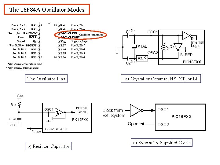
The 16 F 84 A Oscillator Modes The Oscillator Pins b) Resistor-Capacitor a) Crystal or Ceramic, HS, XT, or LP c) Externally Supplied Clock
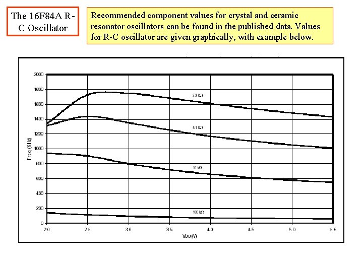
The 16 F 84 A RC Oscillator Recommended component values for crystal and ceramic resonator oscillators can be found in the published data. Values for R-C oscillator are given graphically, with example below.
The 16 F 84 A Power Supply The power supply connections are easily seen on the pin connection diagram. It is easy to get these mixed up – don’t!
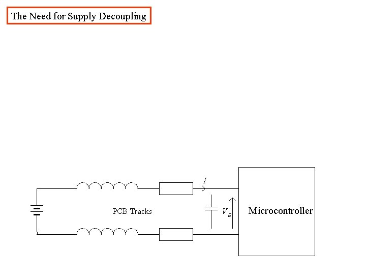
The Need for Supply Decoupling I PCB Tracks Vs Microcontroller
The Hardware Design of the Electronic Pingpong End of Lecture Note
- Slides: 21