Designing Embedded Systems with PIC Microcontrollers Principles and
Designing Embedded Systems with PIC Microcontrollers: Principles and Applications 2 nd Edition. Tim Wilmshurst Chapter 7 Larger Systems and the PIC 16 F 873 A The aims of this chapter are to introduce: • The architecture of the 16 F 873 A microcontroller; • The 16 F 873 A memory map; • The 16 F 873 A interrupt structure; • The use of the Microchip in-circuit debugger. Instructors using Designing Embedded Systems with PIC Microcontrollers are welcome to use or change these slides as they see fit. Feedback, to t. j. wilmshurst@derby. ac. uk, is welcomed. The copyright to all diagrams is held by Microchip Technology, or T. Wilmshurst, unless otherwise stated
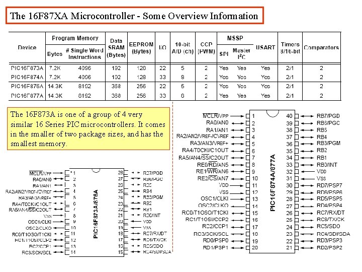
The 16 F 87 XA Microcontroller - Some Overview Information The 16 F 873 A is one of a group of 4 very similar 16 Series PIC microcontrollers. It comes in the smaller of two package sizes, and has the smallest memory.
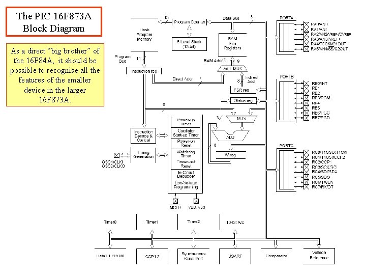
The PIC 16 F 873 A Block Diagram As a direct “big brother” of the 16 F 84 A, it should be possible to recognise all the features of the smaller device in the larger 16 F 873 A.
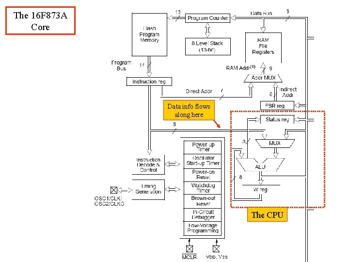
The 16 F 873 A Core Data info flows along here The CPU
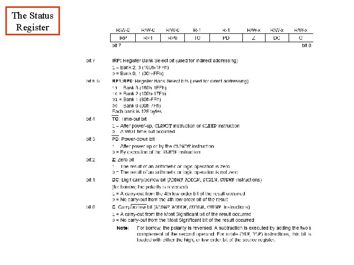
The Status Register
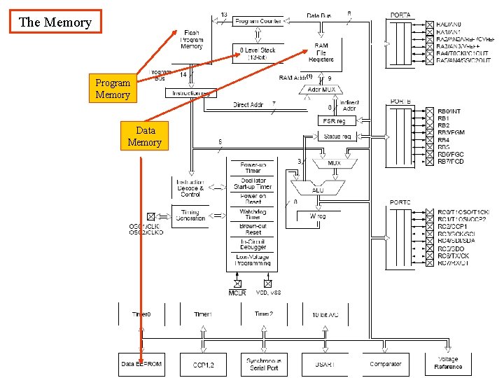
The Memory Program Memory Data Memory
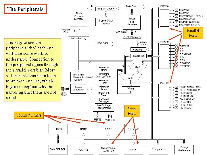
The Peripherals Parallel Ports It is easy to see the peripherals, tho’ each one will take some work to understand. Connection to the peripherals goes through the parallel port bits. Most of these bits therefore have more than one use, which begins to explain why the names against them are not simple. Counter/Timers Serial Ports
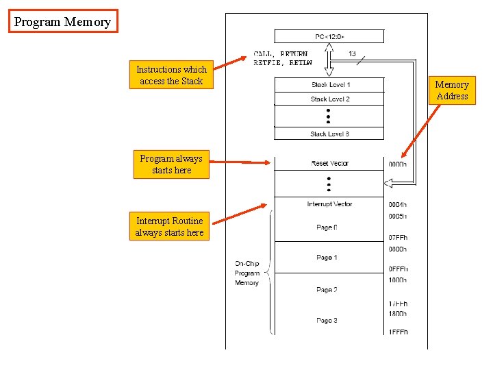
Program Memory Instructions which access the Stack Program always starts here Interrupt Routine always starts here Memory Address
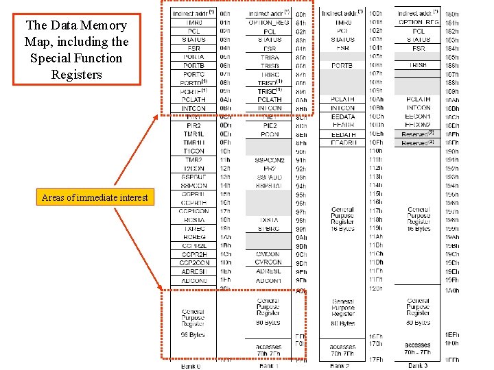
The Data Memory Map, including the Special Function Registers Areas of immediate interest
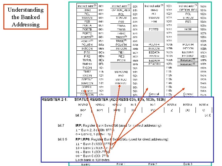
Understanding the Banked Addressing
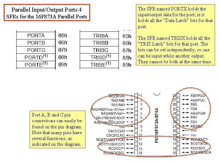
Parallel Input/Output Ports 4 SFRs for the 16 F 873 A Parallel Ports The SFR named PORTX holds the input/output data for the port, ie it holds all the “Data Latch” bits for that port. The SFR named TRISX holds all the “TRIS Latch” bits for that port. The bits can be set independently, so one can be input while another output. They cannot be both at the same time. Port A, B and C pin connections can easily be found on the pin diagram. Note that many pins have several functions, as indicated on the diagram.
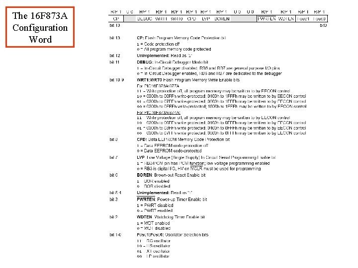
The 16 F 873 A Configuration Word
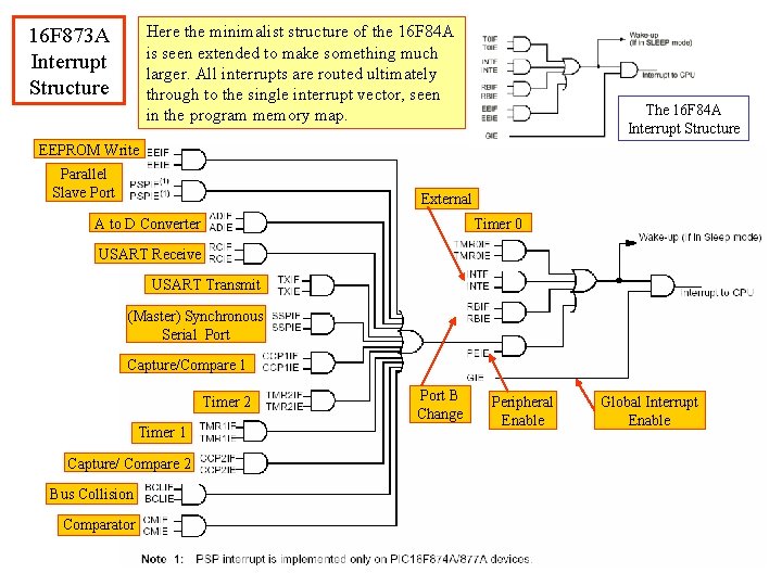
Here the minimalist structure of the 16 F 84 A is seen extended to make something much larger. All interrupts are routed ultimately through to the single interrupt vector, seen in the program memory map. 16 F 873 A Interrupt Structure The 16 F 84 A Interrupt Structure EEPROM Write Parallel Slave Port External A to D Converter Timer 0 USART Receive USART Transmit (Master) Synchronous Serial Port Capture/Compare 1 Timer 2 Timer 1 Capture/ Compare 2 Bus Collision Comparator Port B Change Peripheral Enable Global Interrupt Enable
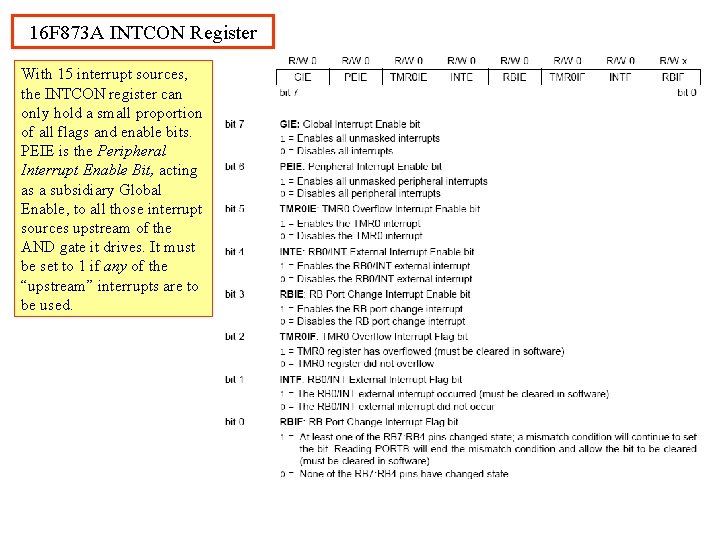
16 F 873 A INTCON Register With 15 interrupt sources, the INTCON register can only hold a small proportion of all flags and enable bits. PEIE is the Peripheral Interrupt Enable Bit, acting as a subsidiary Global Enable, to all those interrupt sources upstream of the AND gate it drives. It must be set to 1 if any of the “upstream” interrupts are to be used.
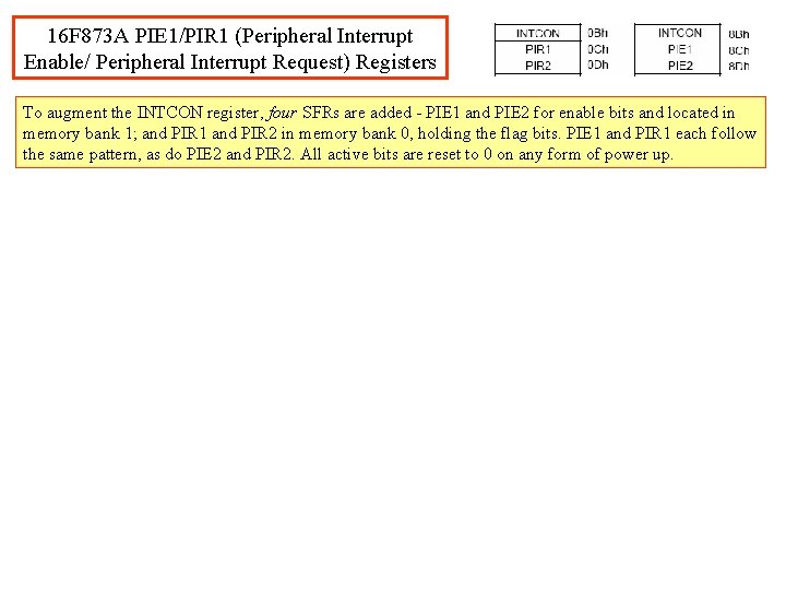
16 F 873 A PIE 1/PIR 1 (Peripheral Interrupt Enable/ Peripheral Interrupt Request) Registers To augment the INTCON register, four SFRs are added - PIE 1 and PIE 2 for enable bits and located in memory bank 1; and PIR 1 and PIR 2 in memory bank 0, holding the flag bits. PIE 1 and PIR 1 each follow the same pattern, as do PIE 2 and PIR 2. All active bits are reset to 0 on any form of power up.

16 F 873 A PIE 2/PIR 2 Registers
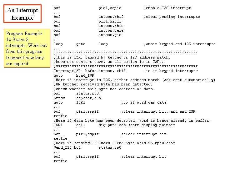
An Interrupt Example Program Example 10. 3 uses 2 interrupts. Work out from this program fragment how they are applied. bsf pie 1, sspie ; enable I 2 C interrupt. . . bcf intcon, rbif ; clear pending interrupts bcf pir 1, sspif bsf intcon, rbie bsf intcon, peie bsf intcon, gie. . . loop goto loop ; await keypad and I 2 C interrupts. . . ; ******************************** ; This is ISR, caused by keypad or I 2 C address match. ; Does not context save, as all action is in ISRs. ; ******************************** Interrupt_SR btfsc intcon, rbif ; is it keypad interrupt? goto kpad_ISR ; Here if interrupt is I 2 C, either address match (Ack sent automatically) ; OR further received byte has been detected. ; check whether this byte was address or data bsf status, rp 0 btfsc sspstat, d_a goto ISR 1 ; go if word was data. . . bcf pir 1, sspif ; clear interrupt bit, and end ISR retfie ; Here if data byte has been detected, word is hence already in buffer. ISR 1 call dig_pntr_set ; sort display pointer. . . bcf pir 1, sspif ; clear interrupt bit retfie ; here if sending I 2 C word. Send byte held in kpad_char Send_I 2 C bcf status, rp 0. . . bcf pir 1, sspif ; clear interrupt bit retfie
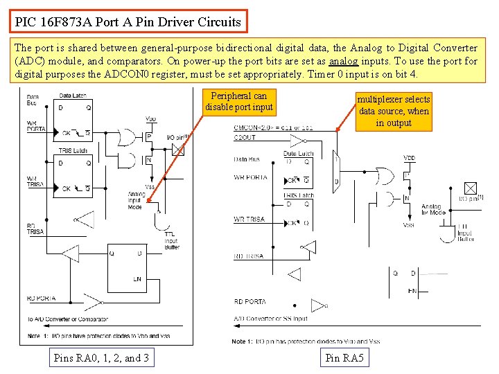
PIC 16 F 873 A Port A Pin Driver Circuits The port is shared between general-purpose bidirectional digital data, the Analog to Digital Converter (ADC) module, and comparators. On power-up the port bits are set as analog inputs. To use the port for digital purposes the ADCON 0 register, must be set appropriately. Timer 0 input is on bit 4. Peripheral can disable port input Pins RA 0, 1, 2, and 3 multiplexer selects data source, when in output Pin RA 5
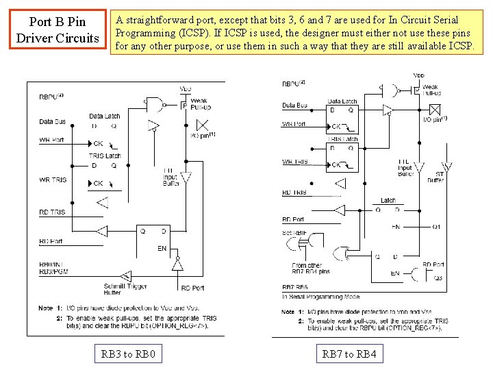
Port B Pin Driver Circuits A straightforward port, except that bits 3, 6 and 7 are used for In Circuit Serial Programming (ICSP). If ICSP is used, the designer must either not use these pins for any other purpose, or use them in such a way that they are still available ICSP. RB 3 to RB 0 RB 7 to RB 4
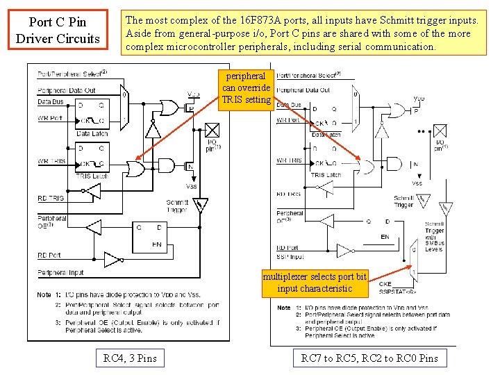
Port C Pin Driver Circuits The most complex of the 16 F 873 A ports, all inputs have Schmitt trigger inputs. Aside from general-purpose i/o, Port C pins are shared with some of the more complex microcontroller peripherals, including serial communication. peripheral can override TRIS setting multiplexer selects port bit input characteristic RC 4, 3 Pins RC 7 to RC 5, RC 2 to RC 0 Pins
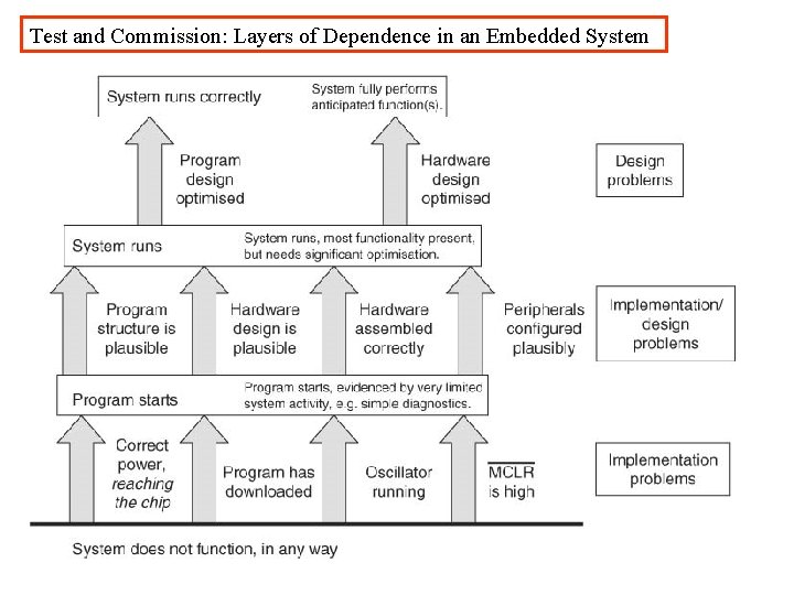
Test and Commission: Layers of Dependence in an Embedded System
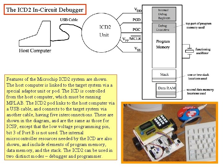
The ICD 2 In-Circuit Debugger Features of the Microchip ICD 2 system are shown. The host computer is linked to the target system via a special adaptor unit or pod. The ICD is controlled from the host computer, which must be running MPLAB. The ICD 2 pod links to the host computer via a USB cable, and connects to the target system via another cable, having five interconnections. These are shown in the diagram, and are the same as those for ICSP, except that the low voltage programming pin, bit 3 of Port B is not used. The internal microcontroller resources needed by the ICD are also shown, and include elements of program memory, data memory, and the stack. The ICD 2 can be used in two distinct modes – debugger and programmer.
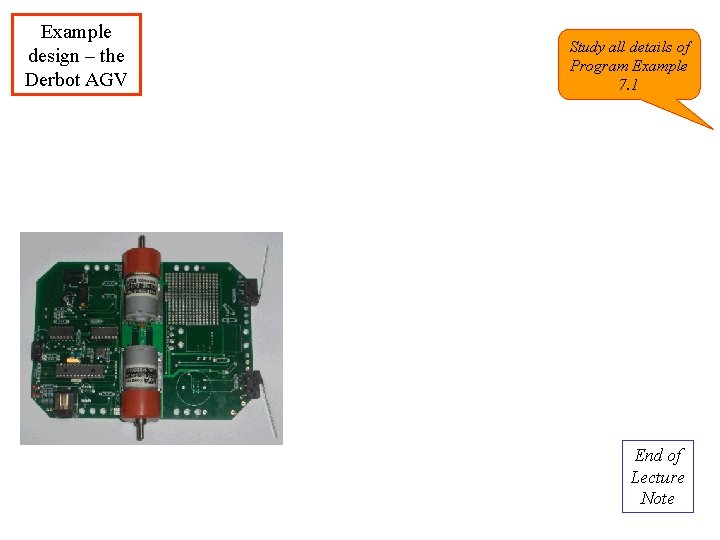
Example design – the Derbot AGV Study all details of Program Example 7. 1 End of Lecture Note
- Slides: 23