DesignInduced Latency Variation in Modern DRAM Chips Characterization


![Challenges of Lowering Latency • Static DRAM latency (e. g. , AL-DRAM [HPCA 2015])](https://slidetodoc.com/presentation_image/434b0e7d81b82e5e0e5aa8276d866962/image-22.jpg "Challenges of Lowering Latency • Static DRAM latency (e. g. , AL-DRAM [HPCA 2015])")


 Smallsmall leakage Cells store charge at. Large high leakage")


")

 4000 3500 3000 2500")
 Random Errors 4000 8300")


 56")


- Slides: 63
Design-Induced Latency Variation in Modern DRAM Chips: Characterization, Analysis, and Latency Reduction Mechanisms Donghyuk Lee 1, 2 Samira Khan 3 Lavanya Subramanian 2 Saugata Ghose 2 Rachata Ausavarungnirun 2 Gennady Pekhimenko 4 Vivek Seshadri 4 Onur Mutlu 5, 2 1 NVIDIA 3 University 2 Carnegie of Virginia Mellon University 4 Microsoft Research 5 ETH Zürich June 7, 2017
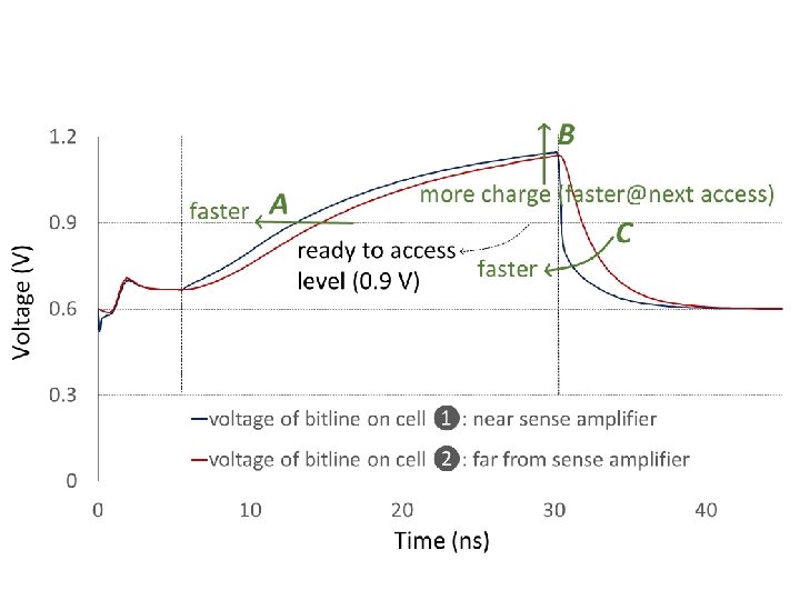
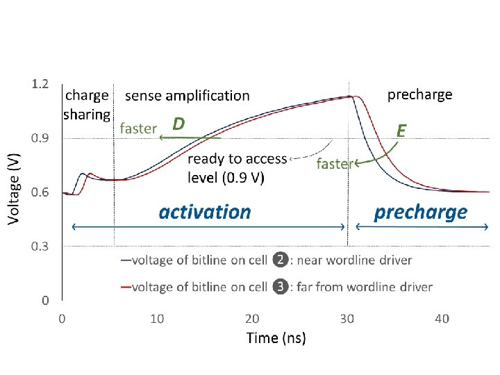
What Is Design-Induced Variation? fast across column slow wordline drivers slow distance from wordline driver across row distance from sense amplifier fast Inherently fast inherently slow sense amplifiers Systematic variation in cell access times caused by the physical organization of DRAM 2
Executive Summary • Design-Induced Variation – Inherently slow regions due to DRAM cell array organization – Goal: Use design-induced variation to reduce DRAM latency • Analysis: Characterization of 96 real DRAM modules – Three types of systematic variation due to design – Great potential to reduce DRAM latency at low cost • Our Approach: DIVA-DRAM – DIVA Profiling: Reliably reduce DRAM latency • Profile only cells in inherently slow regions • Use error correction (ECC) for slow cells that are not profiled – DIVA Shuffling: Exploit variation to improve ECC reliability • 15. 1%/14. 2% higher performance for 2 -/8 -core workloads 3
Presentation Outline • DRAM Background • Experimental Study of Design-Induced Variation – Goal: Understand, identify inherently slower regions – Methodology: Profile 96 real DRAM modules by using FPGA-based DRAM test infrastructure • Exploiting Design-Induced Variation – DIVA Profiling: Using low-cost slow region profiling to reliably and dynamically reduce DRAM latency – DIVA Shuffling: Using variation across data bursts to reduce uncorrectable errors 4
High-Level DRAM Organization memory channel: 64 -bit data bus 8 -bit data bus per chip DRAM chip data burst 8 chips X 8 bits X 8 bursts = 64 bytes Processor Read request DIMM dual in-line memory module 5
Organization Inside a DRAM Chip DRAM mat row group wordline drivers row decoder DRAM cell global wordline sense amplifiers 6
DRAM Operations • Memory controller sends commands to DRAM row decoder column • Activation: Open one row in each mat – Row decoder, wordline drivers select a row of cells – Each cell in the row shares charge with a sense amplifier • Read: Send one column of data from sense amplifiers to CPU • Precharge: Prepare mats for next row • Timing parameters: how long to wait for each step to finish 7
DRAM Timing Parameters • Standard timing parameters are dictated by the worst case • Must ensure reliable operation for: – The smallest cell with the smallest charge in all DRAM modules (process variation) – The highest operating temperature allowed (charge leakage ) • Large for the common Cantiming we usemargin design-induced variationcase and Goal: common-case to find use. Lower common-case latency at low cost? 8
Presentation Outline • DRAM Background • Experimental Study of Design-Induced Variation – Goal: Understand, identify inherently slower regions – Methodology: Profile 96 real DRAM modules by using FPGA-based DRAM test infrastructure • Exploiting Design-Induced Variation – DIVA Profiling: Using low-cost slow region profiling to reliably and dynamically reduce DRAM latency – DIVA Shuffling: Using variation across data bursts to reduce uncorrectable errors 9
Expected DRAM Characteristics • Variation – Some regions are slower than others – If we reduce DRAM latency, slower regions are more vulnerable to errors • Repeatability – Latency (error) characteristics repeat periodically, if the same component (e. g. , mat) is duplicated • Similarity – Characteristics repeat across different organizations (e. g. , chip/DIMM) that share same design 10
Characterization Methodology • We use error behavior when we reduce latency to infer DRAM organization and characteristics – FPGA-based memory controller infrastructure 11
DRAM Testing Infrastructure Temperature Controller FPGAs Heater FPGAs PC Tested 96 DIMMs from three vendors 12
Characterization Methodology • We use error behavior when we reduce latency to infer DRAM organization and characteristics – FPGA-based memory controller infrastructure – We reverse engineer row address mapping – Lower t. RP (precharge timing parameter) to 7. 5 ns • We characterize three types of variation – Variation across columns – Variation across rows – Variation across data bursts • Data and circuit model will be available on Git. Hub: https: //github. com/CMU-SAFARI/DIVA-DRAM 13
1. Variation Across Rows darker cells are faster row group 512 rows sweep across row decoder global wordline Latency characteristics vary across 512 rows Samecharacteristics organization repeats every 512512 rows Latency repeat every 14
1. 2. Periodic Row Variation Behavior 20 18 16 14 12 10 8 6 4 2 0 0 64 128 192 256 320 384 448 512 576 640 704 768 832 896 960 1024 1088 1152 1216 1280 1344 1408 1472 1536 Erroneous Request Count Sorting with Discovered Row Mapping sorted row address Row error (latency) characteristics periodically repeat every 512 rows 15
2. Variation Across Columns darker cells are faster row decoder global wordline Column latency depends on distance from row decoder, wordline driver 16
Erroneous Request Count 2. Variation Across Columns 50 50 40 40 30 30 20 20 10 10 0 32 64 96 Column error (latency) characteristics have specific patterns that repeat across row groups 17
3. Variation Across Data Bursts Processor Read request 64 -bit data bus in memory channel 8 -bit data bus per chip 64 -bit data from different locations in the same row in the same chip DIMM G H D A B C EF G H D A B C EF Chip 1 Chip 2 Chip 3 Chip 4 Chip 5 Chip 6 Chip 7 Chip 8 18
3. Variation Across Data Bursts 35000 Error Count 30000 25000 chip 1 chip 2 chip 3 chip 4 chip 5 chip 6 chip 7 chip 8 20000 15000 10000 5000 0 0 A 8 B 16 C 24 D 32 E 40 F 48 G 56 H data bits in 8 data bursts Specific bits in a request induce more errors 19
Summary: Design-Induced Variation • Systematic variation across rows – Slow cells further from sense amplifier • Systematic variation across columns – Slow cells further from row decoder – Slow cells further from wordline driver • Systematic variation across data bursts – Slow cells at certain bits in a burst – Clustering of errors Can we use design-induced variation to find and use common-case latency at low cost? 20
Presentation Outline • DRAM Background • Experimental Study of Design-Induced Variation – Goal: Understand, identify inherently slower regions – Methodology: Profile 96 real DRAM modules by using FPGA-based DRAM test infrastructure • Exploiting Design-Induced Variation – DIVA Profiling: Using low-cost slow region profiling to reliably and dynamically reduce DRAM latency – DIVA Shuffling: Using variation across data bursts to reduce uncorrectable errors 21
Challenges of Lowering Latency • Static DRAM latency (e. g. , AL-DRAM [HPCA 2015]) – DRAM vendors need to provide fixed timings, increasing testing costs – Doesn’t account for latency changes over time (e. g. , aging and wear out) • Conventional online profiling – Takes long time (high cost) to profile all DRAM cells Our Goal: Use design-induced variation to minimize profiling 22
1. DIVA Profiling Design-Induced-Variation-Aware wordline driver inherently slow sense amplifier Profile only slow regions to determine latency 23
What About Process Variation? process variation random error wordline driver Design-Induced-Variation-Aware slow cells error-correcting codes (ECC) inherently slow architectural variation localized error online profiling sense amplifier Combine ECC & online profiling Reliably reduce DRAM latency at low cost 24
Correction with Conventional ECC Processor Read request 64 -bit data bus in memory channel 8 -bit data bus per chip DIMM Error-Correcting Code (ECC) 25
Challenge of Conventional ECC Processor error DIMM 8 -bit data bus per chip uncorrectable by ECC Clusters of slow cells due to design-induced variation lead to more uncorrectable errors 26
2. DIVA Shuffling Design-Induced-Variation-Aware Processor error DIMM 8 -bit data bus per chip uncorrectable by ECC How do DIVA Profiling and DIVA Shuffling perform? Shuffle data bursts Reduce uncorrectable errors 27
Fraction of Errors Removed DIVA Shuffling Improves ECC DIVASuffling ECC w/o AVA 100% DIVASuffling ECC with AVA Uncorrectable 80% 60% 42. 0% 40% 20% 0% 16. 1% 1 2 3 4 5 6 7 8 33 DIMMs average 9 10 11 12 13 14 15 16 17 18 19 20 21 22 23 24 25 26 27 28 29 30 31 32 33 34 35 36 DIVA Shuffling uses architectural variation to improve error correction using the same codeword 28
DIVA-DRAM Reduces Latency Read Latency Reduction 50% 40% 31. 2% 30% 35. 1%34. 6%36. 6%35. 8% 25. 5% 50% 40% 36. 6% 30% 20% 10% 0% 0% Write 39. 4%38. 7%41. 3%40. 3% 27. 5% 55°C 85°C aggressively 55°C 85°C 55°C latency 85°C DIVA-DRAM reduces more AL-DRAM AVA AVA Profiling DIVAProfiling DIVA + Shuffling and uses ECC to correct random slow cells How do DRAM latency reductions translate to system performance? 29
DIVA-DRAM Improves Performance • 32 single-core benchmarks: SPEC, Stream, TPC, GUPS • 96 multicore workloads constructed with benchmarks AL-DRAM DIVAProfiling AVA DIVAProfiling + Shuffling AVA System Performance Improvement 20% 14. 7%15. 1% 15% 11. 7% 9. 2% 9. 5% 10% 13. 7%14. 2% 11. 0% 13. 8%14. 1% 11. 5% 7. 0% 5% 0% DIVA-DRAM outperforms the best prior work 4 -core changes 8 -core and can 1 -core adapt to 2 -core dynamic latency 30
Conclusion • Design-Induced Variation: Inherently slow regions due to DRAM cell array organization • Analysis: Characterization of 96 real DRAM modules – Three types of systematic variation due to design – Great potential to reduce DRAM latency at low cost • Our Approach: DIVA-DRAM – DIVA Profiling: Reliably reduce DRAM latency • Profile only cells in inherently slow regions • Use error correction (ECC) for slow cells that are not profiled – DIVA Shuffling: Exploit variation to improve ECC reliability • 15. 1%/14. 2% higher performance for 2 -/8 -core workloads 31
Design-Induced Latency Variation in Modern DRAM Chips: Characterization, Analysis, and Latency Reduction Mechanisms Donghyuk Lee 1, 2 Samira Khan 3 Lavanya Subramanian 2 Saugata Ghose 2 Rachata Ausavarungnirun 2 Gennady Pekhimenko 4 Vivek Seshadri 4 Onur Mutlu 5, 2 1 NVIDIA 3 University 2 Carnegie of Virginia Mellon University 4 Microsoft Research 5 ETH Zürich Data, Circuit Model Will Be Available at https: //github. com/CMU-SAFARI/DIVA-DRAM
Backup Slides 33
DRAM 34
Sending Data From a DRAM Chip row decoder global sense amplifiers 64 bits IO interface 8 bits X 8 bursts Data in a request transferred as multiple data bursts 35
DRAM Stores Data as Charge DRAM cell Three steps of charge movement 1. Sensing 2. Restore 3. Precharge Sense amplifier 36
DRAM Charge over Time cell charge Data 1 Sense amplifier Timing Parameters Sensing In theory In practice Data 0 Restore margin time Why does DRAM need the extra timing margin? 37
Two Reasons for Timing Margin 1. Process Variation – DRAM cells are not equal – Leads to extra timing margin for cells cell thatcan store large small amount of of charge; 2. Temperature Dependence – DRAM leaks more charge at higher temperature – Leads to extra timing margin when operating at low temperature 38
DRAM Cells are Not Equal Ideal Real Smallest cell Largest cell Same Different Largesize variation in cell size Same charge Different charge Largelatency variation in charge latency Same Different Large variation in access latency 39
Two Reasons for Timing Margin 1. Process Variation – DRAM cells are not equal – Leads to extra timing margin for cells that can store large amount of charge 2. Temperature Dependence – DRAM leaks more charge at higher temperature – Leads to extra timing margin when operating at low temperature 40
Room Temp. Hot Temp. (85°C) Smallsmall leakage Cells store charge at. Large high leakage temperature and large charge at low temperature Large variation in access latency 41
DRAM Timing Parameters • DRAM timing parameters are dictated by the worst case – The smallest cell with the smallest charge in all DRAM products – Operating at the highest temperature • Large timing margin for the common case Can lower latency for the common case 42
DRAM Timing Parameters Command Data ACTIVATE 1 Activation latency: t. RCD 2 Precharge latency: t. RP (13 ns / 50 cycles) READ PRECHARGE 1111 Cache line (64 B) Duration Next ACT 43 43
Design-Induced Variation in Open Bitline DRAM 44
Challenge: External ≠ Internal DRAM chip Internal address Address mapping IO interface External address ≠ Internal address 45
1 7 1 1 0 6 1 0 1 5 1 0 0 4 0 1 1 3 0 1 0 2 0 0 1 1 1 7 1 1 0 6 0 1 1 5 0 1 0 4 1 0 0 3 1 0 1 2 0 0 1 1 0 0 high 1 Estimated Mapping External Internal error count 1 Ext. MID Ext. MSB Ext. LSB Ext. MSB Int. MID 4/4 = 100% low Int. MSB Int. MID Int. LSB near distance from s/a far DRAM-Internal vs. DRAM-External Ext. LSB Int. LSB 3/4 = 75% Ext. MID Int. MSB 4/4 = 100% Estimated Mapping (External Internal) Based on Error Counts for the External Address 46
Confidence Row Address Mapping Confidence 120% 100% 80% 60% 40% 20% 0% Int. MSB Int. LSB
Expected DRAM Characteristics • Variation – Some regions are slower than others – Some regions are more vulnerable than others when accessed with reduced latency • Repeatability – Latency (error) characteristics repeat periodically, if the same component (e. g. , mat) is duplicated • Similarity – Across different organizations (e. g. , chip/DIMM) if they share same design 48
1. 1. Measuring Row Variation Erroneous Request Count Lower t. RP (precharge timing parameter) to 7. 5 ns 4000 3500 3000 2500 2000 1500 1000 500 0 0 64 128 192 256 320 384 448 row address (mod. 512) Need to reverse engineer row address mapping Periodic Errors details in our paper 49
1. 2. Periodic Row Variation Behavior 20 18 16 14 12 10 8 6 4 2 0 0 64 128 192 256 320 384 448 512 576 640 704 768 832 896 960 1024 1088 1152 1216 1280 1344 1408 1472 1536 Erroneous Request Count Sorting with Discovered Row Mapping sorted row address Row error (latency) characteristics periodically repeat every 512 rows 50
1. 1. Measuring Row Variation t. RP (precharge timing parameter) 4000 3500 3000 2500 2000 1500 1000 500 0 0 64 128 192 256 320 384 448 1 0 7. 5 ns Erroneous Request Count 2 0 64 128 192 256 320 384 448 Erroneous Request Count 10. 0 ns row addr. (mod. 512) engineer row address 512)mapping Need to reverse Random Periodic details in our paper Errors 51
1. 1. Variation in Rows 0 row addr. (mod. 512) Random Errors 4000 8300 3500 8200 3000 8100 2500 8000 2000 7900 1500 7800 1000 7700 500 7600 0 7500 0 64 128 192 256 320 384 448 1 Erroneous Request Count 2 7. 5 ns 0 64 128 192 256 320 384 448 Erroneous Request Count 10. 0 ns row addr. (mod. 512) Periodic Errors 5. 0 ns 0 64 128 192 256 320 384 448 t. RP (precharge timing parameter) row addr. (mod. 512) Mostly Errors 52
1. 2. Periodic Row Variation Behavior 3500 3000 2500 2000 1500 1000 500 0 row address (mod. 512) 20 18 16 14 12 10 8 6 4 2 0 0 64 128 192 256 320 384 448 512 576 640 704 768 832 896 960 1024 1088 1152 1216 1280 1344 1408 1472 1536 4000 0 64 128 192 256 320 384 448 512 Erroneous Request Count Aggregated & Sorted Apply sorted order to each 512 -row group row address Error (latency) characteristics periodically repeat every 512 rows 53
2. Variation Across Columns row decoder global wordline column global sense amplifier column 64 bits IO interface 8 bits X 8 bursts Different columns data from different locations different characteristics 54
3. Variation in Data Bits row decoder global sense amplifier 64 bits IO interface 8 bits X 8 bursts Data in a request transferred as multiple data bursts 55
Methodology Modified version of Ramulator (cycle accurate DRAM simulator) 56
Conclusion • Design-Induced Variation exists in DRAM – Inherently slow regions due to DRAM cell array organization – Leads to high DRAM latency • Analysis: Characterization of real DRAM modules – Measured design-induced variation in 96 modules – Great potential to lower DRAM timing parameters • Our Approach: DIVA-DRAM (Design-Induced Variation Aware) – DIVA Profiling: Profile only inherently slow regionsto determine latency dynamic & low-cost latency optimization – DIVA Shuffling: Distribute data from slow regions to different error correction codewords avoid uncorrectable errors • Significant system performance improvement (15% for memory-intensive workloads) 57
Erroneous Request Count 4000 3500 3000 2500 2000 1500 1000 500 0 256 ms 0 64 128 ms 64 ms 128 192 256 320 384 448 Row Address (modulo 512)
Erroneous Request Count 4000 85°C 65°C 45°C 3000 2000 1000 0 0 64 128 192 256 320 384 448 Row Address (modulo 512)
1000 1 K Error Count Ratio 10000 10 K 100 100 1010 10 10 1 11 1234567891011 213141516171819202122 324252627282930313233 435363738394041424344 546474849505152535455 657585960616263646566 768697071727374757677 879808182838485868788 9 0919293949596 vendor A Company A vendor C vendor B Tested DIMMs Company B Company C 11 1 2 3 4 5 6 7 8 9101112131415161718192021222324252627282930313233343536373839404142434445464748495051525354555657585960616263646566676869707172737475767778798081828384858687888990919293949596 vendor A Company A vendor C vendor B Tested DIMMs Company B Company C
global wordline driver cell capacitor local wordline driver wordline access transistor . . . 2 3 512 rows (cells per bitline) . . . bitline parasitic resistance & capacitance . . . 1 local sense amplifier mat 512 columns (cells per wordline) mat