Design Space Exploration for Minimizing MultiProject Wafer Production

- Slides: 46

Design Space Exploration for Minimizing Multi-Project Wafer Production Cost Rung-Bin Lin (林榮彬) Department of Computer Science and Engineering Yuan Ze University

Outline • • Introduction IC fabrication cost Cost model for MPW Design space exploration for minimal cost MPW fabrication • Experimental results • Summary and future Work

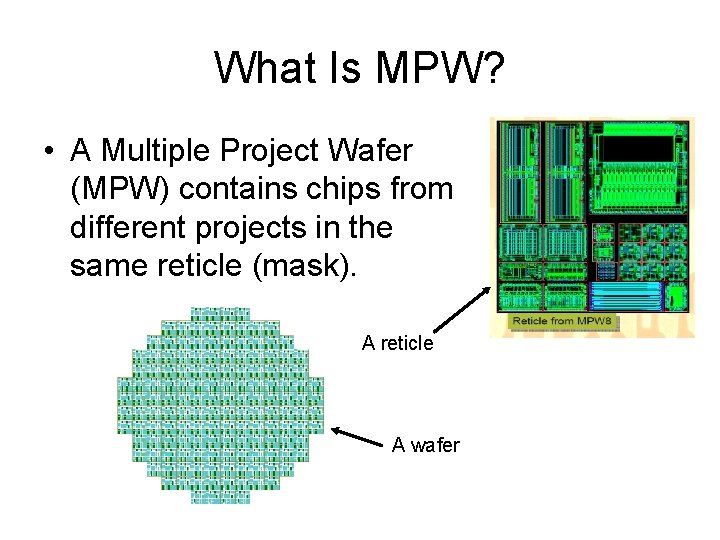
What Is MPW? • A Multiple Project Wafer (MPW) contains chips from different projects in the same reticle (mask). A reticle A wafer

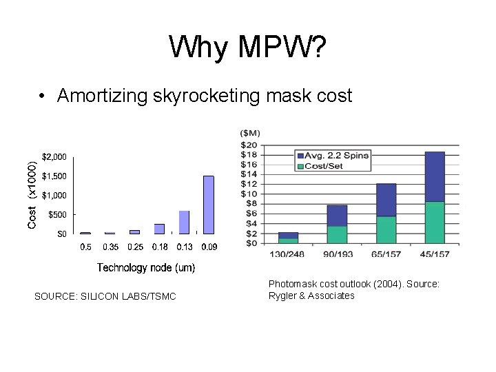
Why MPW? • Amortizing skyrocketing mask cost SOURCE: SILICON LABS/TSMC Photomask cost outlook (2004). Source: Rygler & Associates

Cost of IC Fabrication • Mask cost • Wafer cost – Lithography versus non-lithography cost • Packaging cost • Test cost

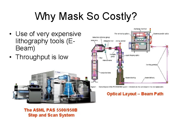
Why Mask So Costly? • Use of very expensive lithography tools (EBeam) • Throughput is low Optical Layout – Beam Path The ASML PAS 5500/950 B Step and Scan System

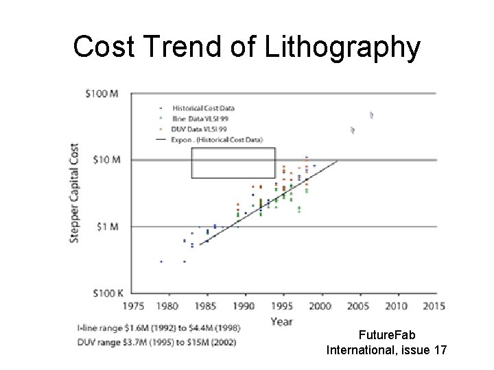
Cost Trend of Lithography Future. Fab International, issue 17

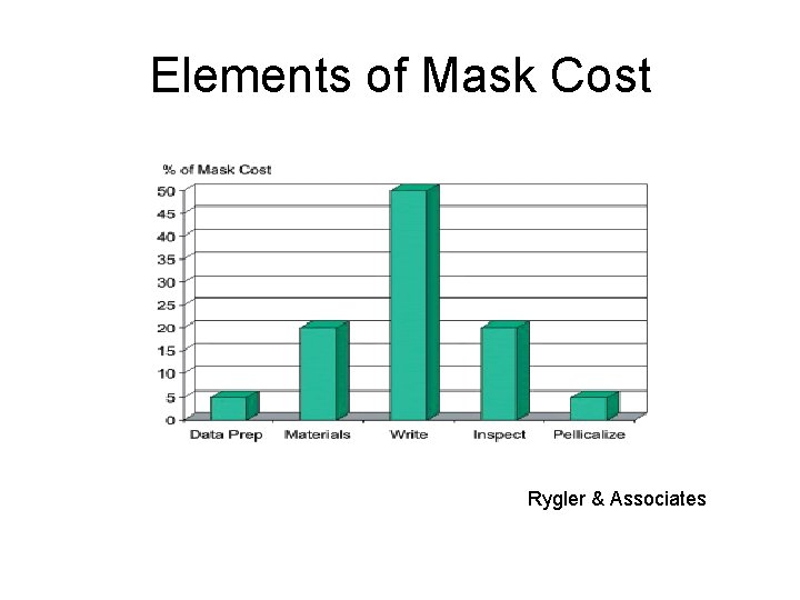
Elements of Mask Cost Rygler & Associates

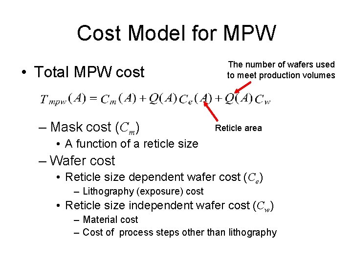
Cost Model for MPW • Total MPW cost – Mask cost (Cm) The number of wafers used to meet production volumes Reticle area • A function of a reticle size – Wafer cost • Reticle size dependent wafer cost (Ce) – Lithography (exposure) cost • Reticle size independent wafer cost (Cw) – Material cost – Cost of process steps other than lithography

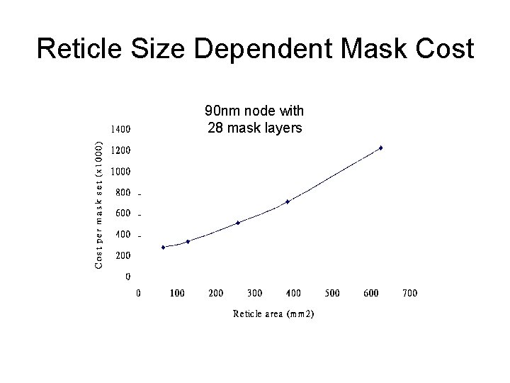
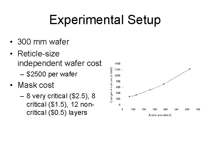
Reticle Size Dependent Mask Cost 90 nm node with 28 mask layers

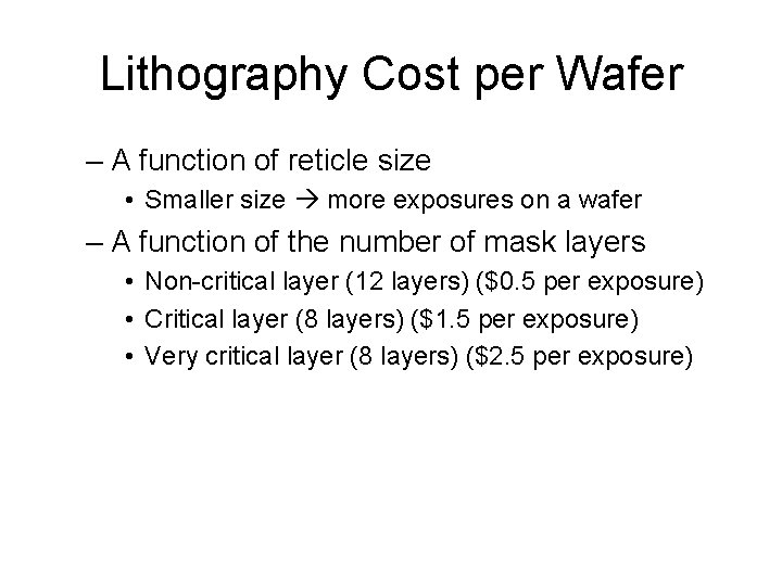
Lithography Cost per Wafer – A function of reticle size • Smaller size more exposures on a wafer – A function of the number of mask layers • Non-critical layer (12 layers) ($0. 5 per exposure) • Critical layer (8 layers) ($1. 5 per exposure) • Very critical layer (8 layers) ($2. 5 per exposure)

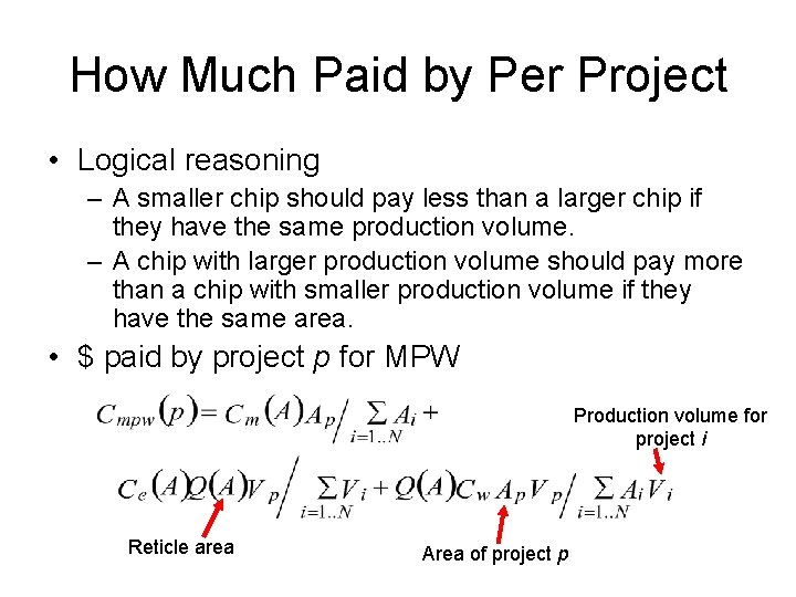
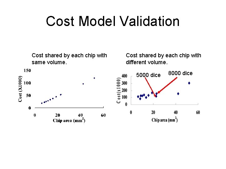
How Much Paid by Per Project • Logical reasoning – A smaller chip should pay less than a larger chip if they have the same production volume. – A chip with larger production volume should pay more than a chip with smaller production volume if they have the same area. • $ paid by project p for MPW Production volume for project i Reticle area Area of project p

Cost Model Validation Cost shared by each chip with same volume. Cost shared by each chip with different volume. 5000 dice 8000 dice

Problem of Minimizing MPW Cost • Given – N chips with areas A 1, A 2, …, AN – Required production volumes V 1, V 2, …, VN • Decide – The coordinates of the chips in a reticle • Objective – Minimize total MPW fabrication cost • Constraints – No chips overlap and all chips are inside the reticle – Smaller than maximally allowable reticle size

Minimizing Total MPW Cost • Minimizing mask cost – Can be decided easily for a given reticle size • Minimizing wafer cost – Need dicing to know the total of number wafers used • These two objectives are conflicting to some certain extent – A balance between mask cost and wafer cost is needed

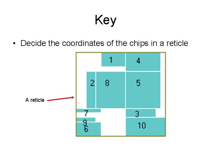
Key • Decide the coordinates of the chips in a reticle A reticle

Reticle Floorplanning Problem (RFP) • Given – N chips with areas A 1, A 2, …, AN – Required production volumes V 1, V 2, …, VN • Decide – The coordinates of the chips in a reticle • Objective – Minimize total number of wafers used • Constraints – No chips overlap and all chips are inside the reticle – Smaller than maximally allowable reticle size

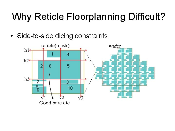
Why Reticle Floorplanning Difficult? • Side-to-side dicing constraints

MPW Wafer Dicing Problem (WDP) • Only way to know the number of wafers used • Given – a reticle floorplan of N chips and the required production volumes • Decide – Dicing lines on each wafer used • Objective – Achieve a minimal number of wafers used • Constraint – Side-to-side dicing constraint

Related Work for RFP • Effective placement of chips on a shuttle mask. Proc. of SPIE, Vol. 5130, 2003, by S. Chen and E. C. Lynn. § B* Tree for reticle area minimization • Shuttle mask floorplanning. Proc. of SPIE. Vol. 5256, 2003, by G. Xu, R. Tian, D. F. Wong, A. J. Reich. § Slicing tree for reticle area minimization (die-to-die inspec. ) • • Chips on Wafer. Proc. of Workshop on Algorithms and Data Structures, 2003, by M. Andersson, J. Gudmundsson, and C. Levcopoulos. § Grid floorplan for maximizing compatibility A multi-objective floorplanner for shuttle mask. Proc. of SPIE. Vol. 5567, 2004, by G. Xu, R. Tian, D. Z. Pan, and D. F. Wong. § Die-to-die inspection, area, wafer utilization, metal density (SA)

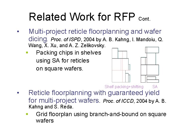
Related Work for RFP Cont. • Multi-project reticle floorplanning and wafer dicing. Proc. of ISPD, 2004 by A. B. Kahng, I. Mandoiu, Q. Wang, X. Xu, and A. Z. Zelikovsky. § Packing chips in shelves using SA for reticles on square wafers. Shelf packing+shifting • SA Reticle floorplanning with guaranteed yield for multi-project wafers. Proc. of ICCD, 2004 by A. B. Kahng and S. Reda. § Grid floorplan using branch-and-bound on square wafers

Related Work for RFP Cont. • CMP aware shuttle mask floorplanning. ASPDAC, 2005 by G. Xu, R. Tian, D. Z. Pan, and D. F. Wong. • Reticle floorplanning and wafer dicing for multiple project wafers. ISQED, 2005, by M. C. Wu and R. B. Lin. – First compatibility- and volume-driven floorplanner • Reticle Floorplanning of Flexible Chips for Multiproject Wafers. GLSVLSI, 2005 by M. C. Wu and R. B. Lin

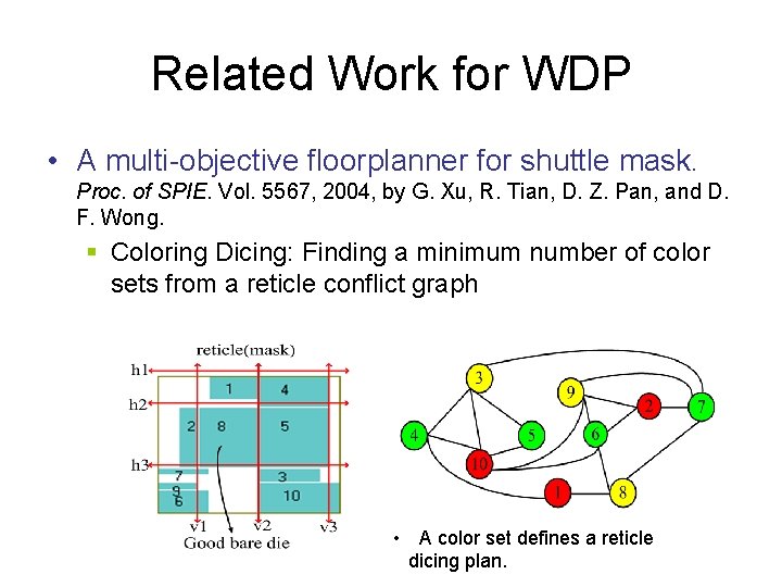
Related Work for WDP • A multi-objective floorplanner for shuttle mask. Proc. of SPIE. Vol. 5567, 2004, by G. Xu, R. Tian, D. Z. Pan, and D. F. Wong. § Coloring Dicing: Finding a minimum number of color sets from a reticle conflict graph • A color set defines a reticle dicing plan.

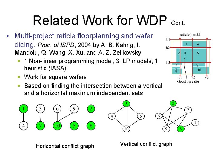
Related Work for WDP Cont. • Multi-project reticle floorplanning and wafer dicing. Proc. of ISPD, 2004 by A. B. Kahng, I. Mandoiu, Q. Wang, X. Xu, and A. Z. Zelikovsky § 1 Non-linear programming model, 3 ILP models, 1 heuristic (IASA) § Work for square wafers § Based on finding the intersection between a vertical and a horizontal maximum independent sets Horizontal conflict graph Vertical conflict graph

Related Work for WDP Cont. • A Comparative study on dicing of multiple project wafers. IEEE CSAS on VLSI, 2005 by M. C. Wu and R. B. Lin – Several dicing ILP models based on coloring reticle conflict graph – One SA implementation based on horizontal and vertical maximum independent sets

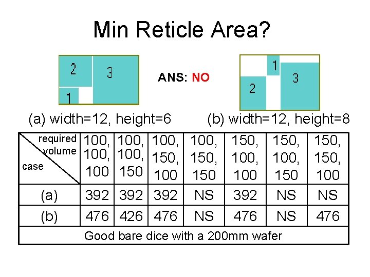
Min Reticle Area? ANS: NO (a) width=12, height=6 required volume case (a) (b) width=12, height=8 100, 150, 100, 150, 100 150 100 392 392 NS NS 476 426 476 NS 476 Good bare dice with a 200 mm wafer

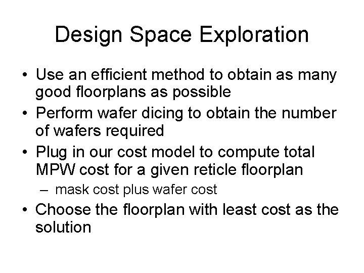
Design Space Exploration • Use an efficient method to obtain as many good floorplans as possible • Perform wafer dicing to obtain the number of wafers required • Plug in our cost model to compute total MPW cost for a given reticle floorplan – mask cost plus wafer cost • Choose the floorplan with least cost as the solution

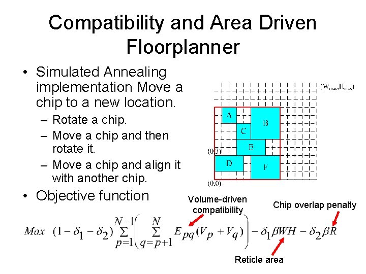
Compatibility and Area Driven Floorplanner • Simulated Annealing implementation Move a chip to a new location. – Rotate a chip. – Move a chip and then rotate it. – Move a chip and align it with another chip. • Objective function Volume-driven compatibility Chip overlap penalty Reticle area

Experimental Setup • 300 mm wafer • Reticle-size independent wafer cost – $2500 per wafer • Mask cost – 8 very critical ($2. 5), 8 critical ($1. 5), 12 noncritical ($0. 5) layers

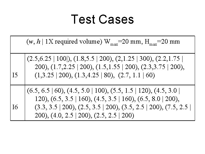
Test Cases (w, h | 1 X required volume) Wmax=20 mm, Hmax=20 mm I 5 I 6 (2. 5, 6. 25 | 100|), (1. 8, 5. 5 | 200), (2, 1. 25 | 300), (2. 2, 1. 75 | 200), (1. 7, 2. 25 | 200), (1. 5, 1. 55 | 200), (2. 3, 3. 75 | 200), (1, 3. 25 | 200), (1. 3, 4. 25 | 80), (2. 7, 1. 1 | 60) (6. 5, 6. 5 | 60), (4. 5, 5. 0 | 100), (5. 5, 1. 5 | 120), (4. 5, 3. 0 | 120), (6. 5, 3. 5 | 160), (4. 5, 3. 5 | 160), (6. 5, 8. 0 | 200), (3. 3, 3. 5 | 200), (2. 5, 3. 5 | 200), (3. 5, 2. 5 | 200), (7. 5, 2. 5 | 200), (4. 0, 2. 5 | 200), (2. 5, 2. 5 | 200)

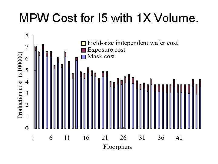
MPW Cost for I 5 with 1 X Volume.

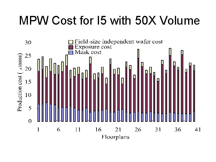
MPW Cost for I 5 with 50 X Volume

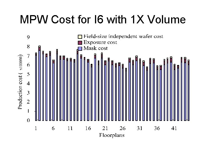
MPW Cost for I 6 with 1 X Volume

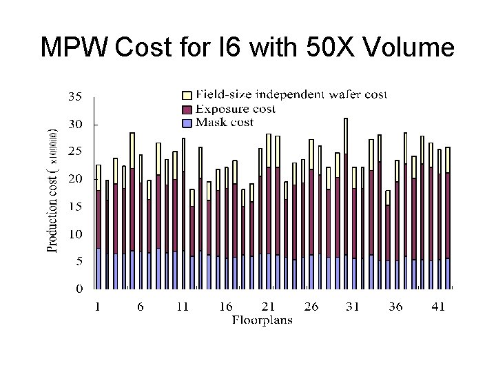
MPW Cost for I 6 with 50 X Volume

Summary • Saving in production cost with a good floorplan – Small volume production (1 X) • 47% for I 5 • 30% for I 6 – Medium volume production • 41% for I 5 • 42% for I 6

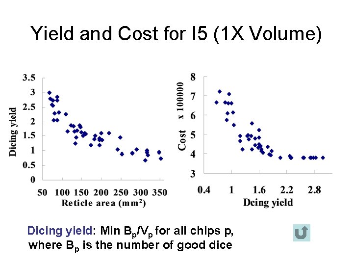
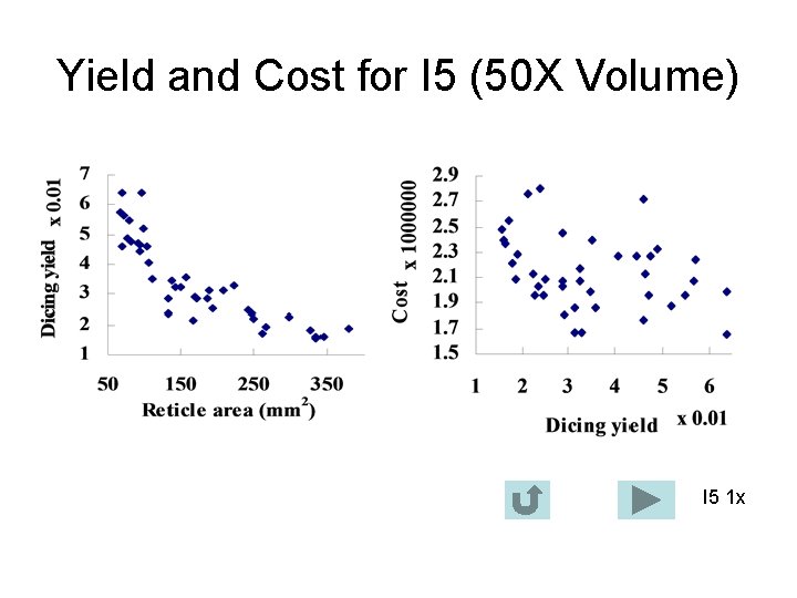
Yield and Cost for I 5 (1 X Volume) Dicing yield: Min Bp/Vp for all chips p, where Bp is the number of good dice

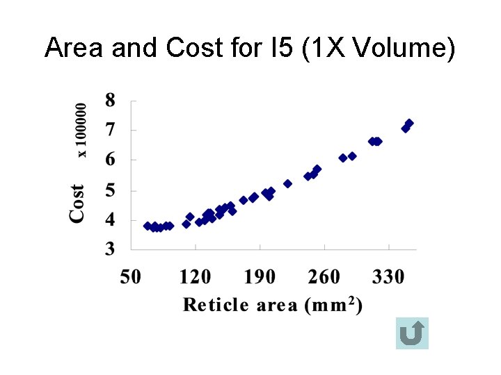
Area and Cost for I 5 (1 X Volume)

Yield and Cost for I 5 (50 X Volume) I 5 1 x

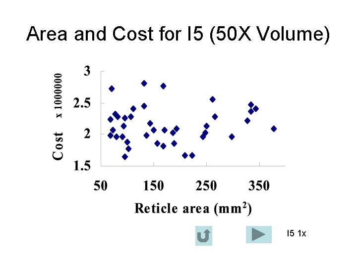
Area and Cost for I 5 (50 X Volume) I 5 1 x

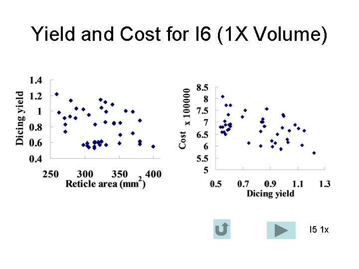
Yield and Cost for I 6 (1 X Volume) I 5 1 x

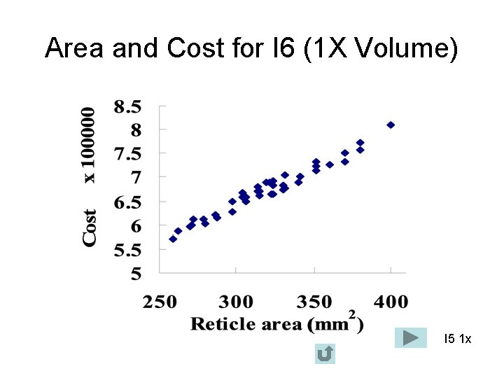
Area and Cost for I 6 (1 X Volume) I 5 1 x

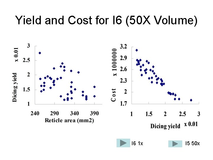
Yield and Cost for I 6 (50 X Volume) I 6 1 x I 5 50 x

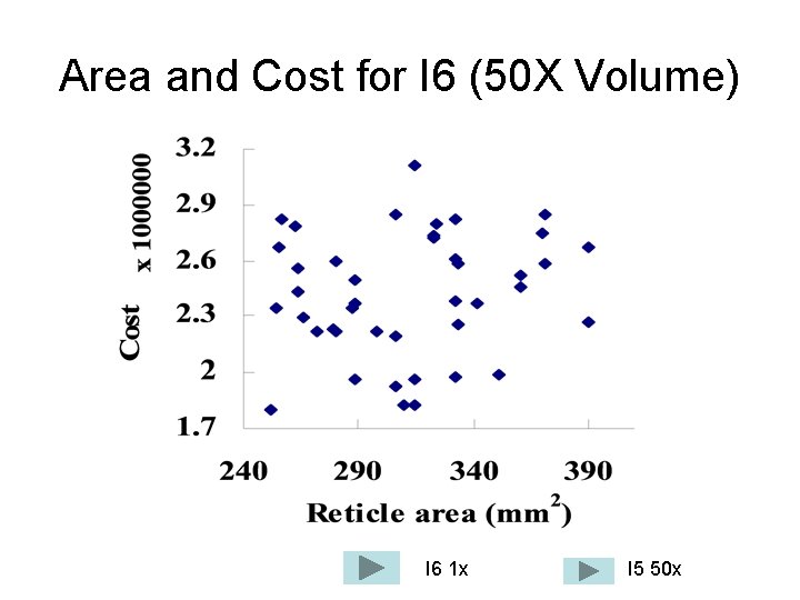
Area and Cost for I 6 (50 X Volume) I 6 1 x I 5 50 x

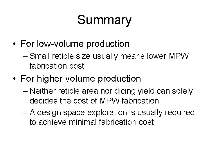
Summary • For low-volume production – Small reticle size usually means lower MPW fabrication cost • For higher volume production – Neither reticle area nor dicing yield can solely decides the cost of MPW fabrication – A design space exploration is usually required to achieve minimal fabrication cost

On Going Work • Floorplanning chips on multiple reticles Taiwan: An Island of Continental Dimensions George Burns, Strategic Marketing Associates, Santa Cruz, Calif. -- 9/1/2003 Semiconductor International

Acknowledgements • The research work presented in this talk is mainly done my student Meng-Chiou Wu. THANK YOU